Model-Based Design for Embedded Systems- P72 pps
Bạn đang xem bản rút gọn của tài liệu. Xem và tải ngay bản đầy đủ của tài liệu tại đây (555.24 KB, 10 trang )
Nicolescu/Model-Based Design for Embedded Systems 67842_C020 Finals Page 696 2009-10-2
Nicolescu/Model-Based Design for Embedded Systems 67842_C021 Finals Page 697 2009-10-2
21
Smart Sensors Modeling Using VHDL-AMS
for Microinstrument Implementation with a
Distributed Architecture
Carles Ferrer, Laura Barrachina-Saralegui, and Bibiana Lorente-Alvarez
CONTENTS
21.1 Introduction 697
21.2 Architecture 698
21.3 Design Methodology for MEMS Design 700
21.4 Application 702
21.5 Accelerometer 704
21.5.1 Description of the Accelerometer 704
21.5.2 Output Circuitry 706
21.5.3 IBIS Drivers 708
21.5.4 Interface of the Accelerometer 711
21.6 Gyroscope . 711
21.7 Smart Sensor Simulation 714
21.7.1 IBIS Drivers in Sensors 714
21.7.2 Interface of the Gyroscope 715
21.8 Simulation and Validation . 717
21.9 Conclusions 717
Acknowledgments 717
References 718
21.1 Introduction
The growing importance of microelectromechanical systems (MEMS) in a
wide range of applications, which combine extreme sensitivity, accuracy,
and compactness, has evidenced the need to simplify the design process
in order to reduce the design time and cost. One of the possible solu-
tions for MEMS design is the extension of the use of an integrated circuit
design methodology to obtain a top-down design methodology that is pos-
sible thanks to the new available mixed-signal modeling languages, such
as VHDL-AMS [1], analog and mixed-signal extension of VHDL language,
697
Nicolescu/Model-Based Design for Embedded Systems 67842_C021 Finals Page 698 2009-10-2
698 Model-Based Design for Embedded Systems
which allows developing models that combine not only digital and analog
signals, but also thermal, mechanical, and optical signals.
The main step in the process of designing for MEMS integration is to com-
bine VHDL models with VHDL-AMS models to obtain a complete descrip-
tion of the multitechnological system. Considering a simplified design flow
for mixed-signal models, the first step will be to define initial specifica-
tions including environment and technical characteristics. The next step is to
define interfaces and partitioning into basic components (including sensors,
actuators, analog, and digital circuitry) to design an abstract structure that
meets the initial requirements. Each component modeling is realized with
the most appropriate language and could be described at different represen-
tation levels (behavioral, structural, circuit, device, and physical) [2,3]. The
modeling of each component becomes a complex task because of the differ-
ent languages and abstraction levels required. Finally, after the fabrication
and/or assembly of all the components, a test and qualification phase must
be carried out in order to guaranty the expected quality levels for the target
application. In one approach, the digital elements have been developed by
using VHDL, while the nonelectronic (transducers) parts and the analog and
mixed-signal circuitry models have been elaborated in VHDL-AMS.
The microinstrument that is modeled and to which this methodology is
applied is an inertial measurement unit (IMU). An IMU is the main com-
ponent of inertial guidance systems used in air-, space-, and watercraft. An
IMU works by sensing motion including the type, rate, and direction of that
motion, and it will be composed of three accelerometers and three gyro-
scopes with all these transducers based on MEMS technology. Additionally,
the necessary processing circuitry and modules for digital communication
have to be treated and modeled with the most suitable language depending
on the nature of the element.
This chapter is structured in the following manner: Section 21.2 presents
the distributed architecture; Section 21.3 deals with the design methodology
for MEMS; Section 21.4 provides an example of an application case based on
an IMU; Sections 21.5 and 21.6 present accelerometer and gyroscope sensor
modeling, respectively; Section 21.7 describes the modeling of a complete
smart sensor including the sensor and their associated electronic circuitry;
Section 21.8 presents simulation and validation results; and Section 21.9
concludes the chapter.
21.2 Architecture
The associated electronic circuitry that measures a sensor must be
considered, and it adds different and necessary functions, such as correcting
offsets, temperature compensations, AD conversions, etc. All these functions
Nicolescu/Model-Based Design for Embedded Systems 67842_C021 Finals Page 699 2009-10-2
Smart Sensors Modeling Using VHDL-AMS 699
Signal conditioning
ProcessingProcessing
Amplification
Actuators Sensors
Amplification
Microcontroller
Driver
Driver
Driver
Driver
FIGURE 21.1
Distributed architecture.
have to be considered from early design phases of a smart sensor. Smart
microsystems can not only process the signal coming from the sensor itself,
they can also have the communication drivers related to these sensors [4].
All nodes or the set of smart sensors are connected to a host (com-
puter or microcontroller) through a sensor bus called interconnection bus
for integrated sensors (IBIS). IBIS was designed for a better serial connec-
tion between the smart sensors and the main controller. The communications
between nodes is established through a designed protocol where each node
is classified into master or slave and has its own logic address [5].
This bus is based on a distributed architecture (see Figure 21.1). The main
advantage of the distributed architecture is that when it has to be extended
because of the increasing number of smart sensors or actuators in a microsys-
tem, additional smart sensors or actuators can easily be connected without
the need to rearchitect. So, one of the solutions found was to specify a dis-
tributed architecture in which a bus sensor was implemented, and this way
a specific interconnection was developed [6].
The distributed architecture introduces the advantage of modularity and
interchangeability as it enables an easy communication applicable to differ-
ent sets of microsystems. Its main characteristic is to own two buses. The
sensor bus is used for relatively short distances, a few centimeters, and for
connecting sensors and actuators on the same subsystem through a dedi-
cated microcontroller. The use of miniature sensors in high numbers raises
the problem of the size and mass of the interfacing cables and connectors,
which are currently much higher than those of the sensors themselves. This
increases the necessity to address the problem of whether it is possible to
reduce, or even eliminate, the mass and volume of the interfacing devices.
An evolution of this second architecture can be seen in Figure 21.2.
It is shown how the master is combined with several elements such as
Nicolescu/Model-Based Design for Embedded Systems 67842_C021 Finals Page 700 2009-10-2
700 Model-Based Design for Embedded Systems
S/A +circuitry
Host
Application bus
S/A +circuitry
S/A +circuitry
Sensor bus
(IBIS)
Application level
Micro instrument level
Several
interfaces
Processor
Memory
SoC bus
Master
SoC level
FIGURE 21.2
Enlarging the architecture.
memory, processor, and interfaces, forming a system on chip (SoC) that
could be implemented with an ASIC or an FPGA, and how they can be inte-
grated in the distributed architecture, combined with a higher lever (appli-
cation level) and the lower level (sensor level) to built up the instrument.
As it is said, IBIS was designed for the better integration of the sensors in
a system. We have decided to create a two-wire low rate synchronous mono-
master bus. This bus can address up to 31 slaves, using the 32nd address to
address all the slaves at the same time, when it is necessary to send a general
reset, to do a self-test, or to initialize the sensors and actuators at the same
time specially. However, any new necessary command that will affect the
entire system could be implemented. The speed of an IBIS is about 1 MHz,
and it has a bus-shaped topology.
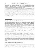
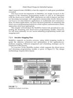
21.3 Design Methodology for MEMS Design
The design of MEMS can often become a task more complex than design-
ing an electronic circuit. This is because MEMS behavior cannot be consid-
ered a simple addition of separate mixed (fluidic, optical, thermal, etc.) and
electrical behavior, but it is a simultaneous combination. This fact motivates
the extension of the existent design methodology for integrated circuits to
obtain a top-down design methodology for MEMS design [7]. It is based on
a hierarchical design method with both abstract behavioral and functional
models in device-analog-digital domain (see Figure 21.3). The development
of a design hierarchy allows the designer to mix levels of abstraction to
observe and evaluate interactions between interdependent subsystems.
Nicolescu/Model-Based Design for Embedded Systems 67842_C021 Finals Page 701 2009-10-2
Smart Sensors Modeling Using VHDL-AMS 701
Sensor/
actuator
Analog
Design of the system
mixed signal verification
Test and qualification
Behavioral model
S/A block design
Block
specifications
Block
specifications
Functional model
functional
Macro
specifications
Spice description
transistor level
design
Gate description
gate level design
Logic
synthesis
Functional
model
RTL level design
Function
synthesis
Behavioral model
digital block
design
Behavioral model
analog block
design
Digital
Functional model
S/A structural
device design
Device
specifications
Fabrication
description
wafer level
design
Physical design Physical design Physical design
Specifications
Defining interfaces
Partitioning
Detailed design
Fabrication or
programming
Assembly
(if necessary)
FIGURE 21.3
Top-down design flow for MEMS.
Nicolescu/Model-Based Design for Embedded Systems 67842_C021 Finals Page 702 2009-10-2
702 Model-Based Design for Embedded Systems
In this design flow, the functionality can be easily verified and analyzed
at the top level. The specifications and characteristics of each stage (sensor/
actuator, analog, digital) can be fixed at a lower level, using specific simu-
lators (such as SPICE for analog circuits) to optimize design at the lowest
level blocks. This phase is very close to the convectional methods used in
MEMS design. The following phases of the design include effects because
of the extension of a top-down “digital” methodology: (a) The verification
of the whole simulation system can be obtained, although it is not possible
to directly synthesize the complete design with VHDL-AMS. (b) Rapid and
easy design process from the top-down. We take physical characterization
into consideration at the final design to validate abstract models developed
in early design stages. (c) Evaluation of the entire system at any design stage.
This is of greater importance in the analog and MEMS design, especially con-
sidering the multitechnolgical nature of MEMS.
In order to obtain the necessary models of the MEMS, there are sev-
eral possible approaches. Generalized networks can be considered in MEMS
modeling because many physical quantities are compared to flow or differ-
ence quantities and generalized Kirchhoff’s laws can be applied. To obtain
a generalized network, large systems can be interpreted as decompositions
into basic network elements. This network concept is valid in many different
domains, such as electrical, fluidic, mechanical, etc.
Another way to obtain the model is using order reduction. Modeling
strategy with the real system can be described using partial differential
equations for the entire system; producing reduced system matrices that
simplify the simulation effort required comparing with the complexity of
the equations that describes the MEMS device functionality. The last way
is to obtain behavioral models as black-box models, derived from simula-
tion results in the time or frequency domain. Once the model is developed
and included in the complete system, the simulation process must consider
a tuning phase through the optimization of parameter settings.
The available modeling tools as well as available multidomain libraries
are usually incomplete. However, many system simulators can support stan-
dardized modeling languages, like VHDL-AMS, and therefore any others in
the near future.
21.4 Application
The case example presented in this work focuses on the development of
a complete behavioral model of an IMU in VHDL-AMS. This IMU com-
bines MEMS sensing technology with analog and digital signal processing
circuitry, all interconnected in a distributed architecture through the bus
IBIS. The system is composed of three accelerometers and three gyroscopes,
one for each direction of space, its conditioning signal circuitry, and the
Nicolescu/Model-Based Design for Embedded Systems 67842_C021 Finals Page 703 2009-10-2
Smart Sensors Modeling Using VHDL-AMS 703
corresponding interfaces to connect them to the communication bus. The
complete system model covers mixed-technology sensors and mixed-signal
circuitry, so it has been developed in VHDL-AMS for the analog and mixed-
technology modules, and VHDL for the digital ones. All these models
have been cosimulated within the same environment following the design
methodology design flow described in Figure 21.3. In this approach, a behav-
ioral description of sensor/actuator and analog circuitry has been chosen in
combination with a more structural description of the digital circuitry parts.
By employing an IMU, it is possible to know the position of an object in
motion, so it has many applications in remote control systems and navigation
systems. An IMU may have many architectures and designs, with different
composing elements, depending on the technology and algorithm employed.
In our case, the IMU is composed of three accelerometers and three gyro-
scopes, each one with its own processing signal circuitry, although it could
be designed using a Kalman filter and gyroscopes. Both designs have been
corrected from early conception to provide an adequate response for the
analog-to-digital converter (ADC). They are basically composed of an ampli-
fier stage and filtering modules to reduce the electrical noise. Finally, to con-
nect each sensor to the communication bus, it has been necessary to develop
an interface to synchronize and make the data types compatible. The IMU
structure is shown in Figure 21.4.
Accelerometer
Accelerometer
Gyroscope
Gyroscope
Accelerometer
Gyroscope
X-axis
Y-axis
Z-axis
Output circuitry
Output circuitry
Output circuitry
Output circuitry
Output circuitry
Interface
Interface
Interface
Interface
Interface
Interface
IBIS
SoC bus
Master
Communication
interfaces
Processor
Memory
Output circuitry
FIGURE 21.4
IMU structure.
Nicolescu/Model-Based Design for Embedded Systems 67842_C021 Finals Page 704 2009-10-2
704 Model-Based Design for Embedded Systems
Different models have been elaborated for each element of the system,
trying to develop behavioral and functional models to be employed in large
simulations, and structural models that allow descending to lower levels of
abstraction. In this way, we obtain a complete description of the system, and
it is thus possible to compare the results of both models in order to improve
them and use the most suitable model in each simulation.
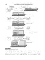
21.5 Accelerometer
The accelerometer that has been assembled as a part of the IMU can be con-
sidered a smart sensor, since it contains the necessary additional circuitry to
connect it to a main controller digital system. The smart sensor is composed
of the acceleration sensor, its output circuitry with an analog-to-digital con-
version, and an interface to adapt the system to a digital device. Its internal
structure is shown in Figure 21.5.
21.5.1 Description of the Accelerometer
The accelerometer is based on the piezoresistive effect, and was built into an
SOI (silicon-on-insulator) wafer packaged on an MCM [8]. It is a Wheatstone
bridge with four piezoresistances placed on a cantilever design, whose value
will depend on the direction of the applied acceleration. We have devel-
oped three different representations of this accelerometer, which will be used
depending on the level of abstraction and the features that we want to study.
The three models are a behavioral model, a physical model, and a mathemat-
ical model.
• The behavioral model of the accelerometer is a simple model that
shows a linear relation between the applied acceleration and the
output voltage. The equation used has been obtained based on the
experimental measurement. This simple model is useful to test other
Accelerometer
Output circuitry
Amplifier stage
CHS
S&H
+
ADC
Interface
IBIS
FIGURE 21.5
Complete system schematic.
Nicolescu/Model-Based Design for Embedded Systems 67842_C021 Finals Page 705 2009-10-2
Smart Sensors Modeling Using VHDL-AMS 705
elements of the sensor, and also to perform simulations that involve
several accelerometers. These simulations could take much time and
resources of the simulator. The model with its simulation can be seen in
Figures 21.6 and 21.7.
• The physical model of the accelerometer takes care of the piezoresistive
effect in the Wheatstone bridge. Given an acceleration, it first calculates
all of the stress applied to the resistances because of this acceleration,
depending on the direction that each resistance is placed. The relation
between the acceleration and the stress is modeled as a linear relation,
whose constants can be obtained through experimental measurement.
Considering the stress applied to each resistance, the next step is calcu-
lating the change in the resistive value. This computation is performed
by applying the known constants for the piezoresistive material of sili-
con for 100 wafers. With this data, the output voltage of the Wheatstone
bridge is easily obtained by applying the characteristic equations of the
system.
entity acc 2_5 v1 is
generic
( Default values for the generics are from D ZU-25g
Static characteristics
Z_in
Z_out
Offset
S_sens
Vdd
N_lin
Hyst
Repet
C_sens_x:real
:real
:real
:real
:real
:real
:real
:real
:real
=
=
=
=
=
=
=
=
=
1888e3;
1882e3;
0.00510;
0.00046;
5.0;
037;
0.12;
0.14;
693;
[Input impedance] = Ohms
[Output impedance] = Ohms
[Offset] = V/V
[Sensitivity] = V/(V.G)
[Voltage supply] = V
[Non-linearity] = %PSO
[Hysteresis] = %PSO
[Repetibility] = %PSO
[X axis cross sensitivity] = %
FIGURE 21.6
Behavioral model for the accelerometer.