21st Century Manufacturing Episode 2 Part 1 ppsx
Bạn đang xem bản rút gọn của tài liệu. Xem và tải ngay bản đầy đủ của tài liệu tại đây (566.07 KB, 20 trang )
'94
Semiconductor Manufacturing Chap. 5
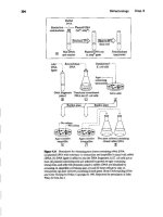
Siwafer
8OO·C-l,200·C
Siwafer
1f O.Ol-1.0I-lmSi02
<hi
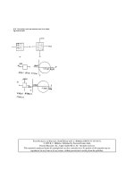
Ftpre5.17
Simplified
viewsof the oxidation
equipment
and
process
(from
Semiconductor Device Fundamentals by Pierret,
©
1996.Reprinted by permission
of Prentice-Hall, Inc., Upper Saddle River, NJ).
However, dry oxygen is again preferred for growing the gate oxide's Si0
2
because it gives better Si to Si0
2
interface properties. Rapid thermal oxidation
(RTO) allows short time oxidation at suitably high temperatures (Campbell, 1996).
5.10.3 Creating Photomasks
The CAD files containing the desired circuit patterns are transferred to a set of pho-
tographic plates or photomasks. To do this, the CAD files are first fed into apattern
generator-a
computer controlled exposure machine. The generator uses flash expo-
sure to transfer the IC pattern onto a light-sensitive plate known as the mask. This
step is similar to photographic developing. The generator flashes onto the plate a
large series of rectangles that correspond to the circuit diagram. The plate is covered
in an emulsion/photoresist material, which deliberately breaks down under the
exposure. Then, once the exposed resist is sloughed off, the plate is transparent just
in those areas that correspond to the circuit.
5.10.4 Photolithography: Projecting the Mask Pattern onto
theWBfer
Many steps follow to transfer the pattern in each photomask to the wafer. The wafer
surface is coated with light-sensitive photoresist material. Typically, photoresist
liquid is poured onto the center of the round wafer, which is spun at 1,000 to 5,000
rpm in order to produce a uniform, thin adhesion. The thickness of the film can be
controlled by altering liquid viscosity and spinning speed. The photoresist is dried in
a warm nitrogen or plain air oven.
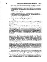
Photolithography is shown in Figures 5.18 through 5.20. In the early days of IC
manufacture, contact and proximity printing were used (Wolf and Tauber, 1986). In
such methods the photomask was in contact with, or very close to. the wafer.
-Quartztube
-Insertionrod
<Resistance-heated furnace
Siw~feT5
Semiconductor Manufacturing Chap. 5
t
Ef3
\
~
~7
r \
~
~7
M:lslep-and-repeat
Ifl step-and-repeat
M:lstep scan
Flame 5.19 Schematics of the different stepper configurations in the lithography
process.
Figure 5.18 is more in keeping with the proximity-type photomask. This shows
(a) a mask at the top, (b) the mask positioned above the photoresist on the wafer,
and (c) the preferentially damaged photoresist on top of the silicon dioxide layer.
During photolithography, ultraviolet (UV) light exposes the photoresist in a
prescribed way,depending on whether a negative or positive resist material is being
used. Positive resists are now the norm in industry because they give better control
for small transistor features. Positive resists contain a sensitizer that normally pre-
vents them from being dissolved away in an alkaline developer solution bath. But if
they are exposed to the UV light that has come through the patterns in the mask, the
sensitizer breaks down. When placed in an alkaline solution, these regions are pref-
erentially removed, leaving a city block-like structure.
In
early
Ie
production, it was also possible to expose many dice at once. One
simultaneous exposure was done with a mask that contained many repeats of the
same pattern. However, as
Ie
features became smaller, it was found difficult to
achieve the registration from one photomask to the next. Also, wafers can get ther-
mally distorted during the intermediate CVD or doping/diffusion steps.
Of course, precise alignment of the wafer and the mask is absolutely essential
for each subsequent layer to match up with the previous one. For that reason, today,
the process is usually fully automated, and one die at a time, or even one area of each
5.10 More Details on Front-End Processing
197
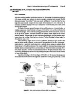
~
~oooo
Mirror
: Hgarclamp
-,' Filter
~~~:~m"I'"
/~ """';' 'V ~
Mask
\, !
\ I
\/
/,
fItue 5.2G Schematic of the reduction
step
lind
repeat technique for projection
printing.
Reduction lens
system
die on the wafer, is exposed. This is the method called projection printing using a lens
system that ismounted well away from the wafer surface. The photomask is inserted
in a step-and-repeat camera, or the optical wafer stepper.1bis transfers the pattern by
beaming a light through the lens system to the photoresist. The images are dernagnl-
tied through the lens down onto the wafers (Figures 5.19 and 5.20).
5.10.5
Etching: Creating the Transistor Channels
Once the pattern is transferred, the light-exposed areas of the photoresist are
removed by developing, and the remaining photoresist is baked to harden and con-
sequently protect the desired pattern underneath, as indicated in Figure 5.11b. Wet
chemical solutions or a dry plasma gas can be used to selectively etch away those
regions of the nitride/oxide barrier layers that are left unprotected. By contrast the
areas of unexposed photoresist protect the underlying areas of the pattern that are
to be temporarily kept in place.
198
Semiconductor Manufacturing Chap. 5
('J
(b)
Si
S.
Figure 5.21 Wet etching (left) creates undercutting as opposed to dry. reactive ion
etching (right) (from Introduction 10 Microelectric Fabrication by Jaeger,© 1988.
Reprinted by permission of Prentice-Hall, Inc., Upper Saddle River, NJ).
Wet etching with a solution containing hydrofluoric acid (HF) creates the val-
leys or windows in nitride/oxide layers. Temperature, time, and solution strength are
monitored carefully so that the nitride/oxide on the substrate is etched quickly, and
yet the photoresist on the other surfaces is not damaged.
Wet etching causesundercutting intothe wallsunderneath thephotoresist,asshown
on the left of Figure 5.21.Thus, although wet etching might still be done in small proto-
typing laboratories,
dry etching
is preferred today for commercial operations because it
does not create the undercutting. It can be done with a variety of plasma beams. For
example,reactive ion etching (RIE) simultaneously attacks the surface with chemical and
physical effects.The plasma is excited in a radio-frequency electric field, and a stream of
reactive ions hits the surface to achieve the followingfor a silicon surface:
• Gases containing fluorine or chlorine interact chemically with a silicon com-
pound and weaken the inherent structure.
•The ions in the plasma have enough energy to knock out the exposed, weak-
ened atoms, thereby eroding the surface.
Note that dry etching may also be used in the later stages to etch patterns into the
aluminum interconnect layers.
An examination of Figure 5.22 shows the result of some of the processing steps:
•The photoresist is protecting a layer of silicide on top of a layer of polysilicon
on top of the silicon wafer (dark gray).
•The protected areas are 0.5 micron wide.
• The unprotected areas are 1.5 microns wide.
• The dry etching prevents undercutting, but there is still some undesirable
tapering of the vertical walls.
• The silicide (TIS
z
)is 0.18 micron thick, and the polysilicon is0.26 micron thick.
5.10.6
Doping: Selectively Isolating the Active Transistor
and Select AreBs
Doping can be accomplished by bombarding the silicon with dopant atoms from
a particle accelerator (ion implantation) followed by further controlled drive-in
diffusion.
Ion implantation uses a high-voltage accelerator to induce dopant atoms into
the wafer surface. Ion implantation is easier to handle than basic diffusion, can be
Resist
~
5.10 More Detailson Front-EndProcessing
'99
Figure 5.22 Result of using photoresist to protect the polysilicon covered
channels 0.5 micron wide (from Device Electron.ics for Integrated Circuits,
Richard S.Muller and Theodore I. Kamins, Copyright © 1986. Reprinted by
permission of John Wiley
&
Sons, Inc.)
more precisely controlled, and allows a wider range of barrier layer materials.
Fig-
ure 5.23 shows that the desired dopant atoms are ionized (bottom right) and then
accelerated by an electric field (center of figure) to energies that typically range from
25 to 200keV When this beam hits the exposed surfaces,the dopant atoms penetrate
the first 1 to 2 microns of the surface layer. This high-energy bombardment in fact
also damages the crystallographic lattice of the silicon. The structure is therefore
annealed, and this also has the effect of locating the dopants at the substitutional
rather than interstitial sites to create n" or
»:
regions.
flpre
5.23 Ion implantation device (adapted from Runyan and Bean.I990).
200
Semiconductor Manufacturing Chap. 5
a-type dopant impurity
FIaure.5.24 The basic diffusion process (from Semiconductor Device
Fundamentals by Pierret, © 1996.Reprinted by permission of Prentice-Hall, Inc.,
Upper Saddle River, NJ).
The ion implantation method allows good control of the dopant concentration:
dopant concentrations are measured in the number of atoms per square centimeter
of surface. High purity of dopants is possible because a mass spectrometer (labeled
analyzer magnet in the figure) near the dopant source acts as a sorting agent,
allowing only the desired dopant species to reach the wafer target.
Also it should be mentioned that ion implantation can penetrate through an
existing layer such as the thin oxide shown in Figures 5.6 and 5.11.Thus additional
doping can be done after the high-temperature cycles that form the Si0
2
•
Muller and
Kamins (1986) and Campbell (1996) provide graphs of depth versus ion energy.
SiwaIers
T",900
a
C-1200"C
Original
p-dopaut
Diffused
~n·dopant
5.10 More Details on Front-End Processing
201
Drive-in diffusion follows ion implantation to create a deeper penetration.
Figure 5.24 schematically shows the diffusion at around
1,OOO"C
of an a-type dopant
into an existing p-type doped substrate. The concentration of dopant is governed by
Fick's law of diffusion (see, for example, Muller and Kamins, 1986).
5.10.7 Chemical Vapor Deposition (CVDI: Creating Layers
for Barriers and Circuits
Thin layers and other materials can be sequentially deposited on the wafer with
chemical vapor deposition (CVD). Out of interest, also note that CVD is used exten-
sively to create hard abrasion-resistant coatings on cutting tools (see Chapter 7).This
involves thermal reactions or breakdowns of gas compounds to coat the substrate.
This is a popular method for depositing barrier layers. Polysilicon, silicon dioxide,
and silicon nitride are routinely deposited using CVD. In Figures 5.25 and 5.26
two CVD processes are shown. The high-capacity, low-pressure (LPCVD) process is
Reactorwalls, 7
(a]
Pressure
[b)
Wafer ""I
load
end cap
ft&me 5.25 Low-pressure CVD (from Device Electronics for Inregrated Circuits,
Richard S.Muller and Theodore I. Kamins, Copyright
©
1986.Reprinted by
permission of John Wiley
&
Sons, Inc.).
Wafers
To
exhaust
3-zoneresistance-
heatedfumancc
Standup wafers
Gas control
system
'Source
gases
Pomp
Trap
202
Semiconductor Manufacturing Chap. 5
Fipre
5.26 Plasma enhanced CVD.
routinely used to deposit Si0
2
and Si
3
N
4
and polysilicon. The diagram shows the
gases flowing around the vertical wafers where surface reaction and diffusion take
place. The plasma enhanced (PECVD) process is chosen because it occurs at lower
temperatures and is well suited to certain operations. For example, the final deposi-
tion of the passivation layer on top of the aluminum interconnections must occur
below 500°Cso that the aluminum does not melt.
A
metallurgical cross section through the films created
by
the CVD methods
reveals amorphous or polycrystalline transitional layers that build from the pure
substrate. By contrast, epitaxy differs from these previous CVD methods because it
is an extension of the underlying crystallography of the substrate. Epitaxy is most
commonly used to grow a thin layer of single crystal silicon onto the silicon wafer.
Vapor phase silicon tetrachloride (SiC4) or silane (SiH
4
)
is used to form additional
silicon on top of a preexisting structure. It is especially useful when needing to grow
a lightly doped layer of silicon on the top of a heavily doped substrate, particularly
in bipolar transistors. It is also useful in CMOS techniques to grow lightly doped
wells on top of existing heavily doped substrates. Vapor phase epitaxy techniques are
described in detail in Campbell (1996, see Chapter 14).
Rotating shaft
Magnetic
rotation
drive
Out to
vacuum
p=p
Heater
Heater
'Electrode
-ShieldedRF
power input
Rotatingsusceptor
O~tto
vacuum
pump
5.10 More Details on Front-End Processing
203
5.10.8 Interconnections and Contacts
To produce a functioning integrated circuit, the millions of transistors and devices
fabricated through the repeated photolithography-etching-doping-deposition cycles
must finally be interconnected. Interconnections are made with metals that adhere
well to substrate materials. Aluminum or aluminum-silicon-copper alloys are gener-
ally used. Copper will increasingly be used to achieve smaller submicron circuit
geometries (Singer, 1997;Braun, 1999). Between two and six layers (shown in Figure
5.27) of metal are deposited over the entire surface of the wafer, with each layer insu-
lated by a dielectric layer. Metal penetrates to the active transistor regions to form
the interconnections to, say, the n
+
region shown on the left of Figure 5.27. The.
second and other layers create circuits between different transistors and devices. Dif-
ferent layers of metal are connected to each other with the vertical channels called
vias, also indicated in the right side of the figure
Sputtering deposits thin films onto the wafer surface in vacuum conditions. A
source of the desired deposition material is bombarded with ions, typically ions of
argon,
AI
+
.1his knocks out atoms from the source, which then sputter onto the wafer
and create the thin film.The general setup for a conductive material such as aluminum
is shown in Figure 5.28.At the top of the chamber. the target is a cathode. The wafers
are mounted on the system's anode in the lower part of the figure.
Evaporation processes can alternatively be used to deposit a thin surface film
on the wafer for the aluminum interconnections. As shown in Figure 5.29, an alu-
minum source is heated and vaporized inside a vacuum chamber. The wafers are
placed like a target opposite this vaporizing source, and with the reduced pressure,
aluminum vapor travels through the chamber to be deposited on the wafer. Careful
control of temperature, atmosphere, and placement isobviously needed to create layers
of even thickness. Several methods are available for heating and vaporizing the source.
• In filament evaporation, short samples of aluminum wire are heated in a tung-
sten boat or are hung from the loops of a resistance-heated tungsten filament.
Resistance heating vaporizes the aluminum source.
• In flash evaporation a spool of the aluminum wire is constantly fed into the
vacuum chamber. A heated ceramic bar vaporizes the incoming wire.
• In electron-beam evaporation, a fixed source isheated andvaporized witha 15keV
"e-beam.vThe
filament and fiash heating methods are subject to the purity of
the source.
F'lgureS.27 Basic two-level
metallization (from
Manufacturing
Processes for Engineering
Malerilll.J
by
Kalpakjian,
©
1m.
Reprinted by
permission of Prentice-Hall, Inc.,
Upper Saddle River, NJ)
Si
Si02
Contact
First-level
metal
Second_level
metBl
Si0
2
204
Semiconductor Manufacturing Chap. 5
Vacuum
chilwber
Cathode shield
Anode
Argon
inlet
Cathode
(sourcemateriaI)
High voltage
~
To
vacuum pump
figure 5.28 Sputtering for the interconnect layers (from Introduction to
Microelecrric Fab,kotwn by Jaeger, © 1988. Reprinted by permission of Prentice-
Hall, Inc., Upper Saddle River, NJ)
/Wafer
Fipe 5.29 Hot
filament evaporation
(from Semiconductor Device
Fundamentals by Pierret, © 1996.
Reprinted by permission of Prentice-
Hall, Iac., Upper Saddle River, NJ).
I
To
vacuum pump
The e-beam method can cause wafer damaging x-rays. In general practice all
these evaporation techniques are less favored in today's commercial tabs. Sput-
tering is used for its superior topological coverage and moderate pressure
requirements.
After the last layer of metal is patterned, a final passivation layer is deposited
in order to protect the [C from contamination and damage. Small openings are then
etched through the layer to expose square aluminum bonding pads, from which wires
will be attached to the package.
Wafers
Heater
Evaporating
"material
5.11 Back-End Processing Methods
205
5.11 BACK·END PROCESSING METHODS
5.11.1 Summary
Wafers are electronically tested for functionality and separated into individual dice.
Each die is set into a chosen package, wire-bonded to the outer perimeter of the
package, and finally tested ready for assembly onto a printed circuit board (PCB).
This segment of semiconductor production is called back-end processing. Figure 5.30
provides an overview of these back-end steps for one of the most common package
types, the dual-in-line package. The single IC is shown on the front right side. It is set
onto the base with epoxy or a metal alloy.The wire bonds (shown darker) run from
bonding pads on the
Ie
to the lead frame of the package. The lead frame connections
go through to the Jcleads or gull-wings that subsequently are attached to the PCB.
The outer cover (labeled molding compound) completes the package.
5.11.2 Testing and Separation
IC designers include special test dice on the wafer that are subjected to all the same
oxidation, etching, layering, and doping processes as the desired Ie. These special test
dice are monitored as much as possible after each of the processing steps described
earlier. At the very end of wafer production these test dice are put through an addi-
tional series of computer-controlled tests in which fine, needlelike probes contact the
aluminum bonding pads of the test dice. If this first check shows that the processing
parameters were within proper limits, then each die is tested for functionality. Dice
that need to be rejected are marked with an ink spot.
After preliminary testing is completed, each die is separated from the wafer,
usually by a diamond saw.In this process the wafer is held down on a sticky sheet of
Mylar and the diamond saw is used either to saw between the dice completely
Molding compound
FigureS.30 Thedual-in-linepackage
(DIP)
(from
Manufacturing Engineering
and Technology 3/e by Kalpakjian,
©
1995.Reprinted by permission
of Prentice-Hall, Inc., Upper Saddle
River,NJ).
Bond wires
-t
Die
Lead frame
Die-support paddl.
Spot plate
2.8
Semiconductor Manufacturing Chap. 5
through the wafer or to scribe the wafer and provide continuous notches. In the latter
approach. the wafer can he turned upside down on a soft pad. A
lightly
pressurized
roller passes across the back of the wafer, and controlled cracks separate the dice.
This method isrelated to the <100> wafer growing direction. In this orientation, nat-
ural cleavage planes run normal to the through thickness direction and to the die
separation lines on the wafer surface. Once all the dice are separated, any inked chips
are discarded, while the remaining chips are inspected visually,under a microscope,
for defects. The die yield from basic wafer production, wafer testing, die separation,
and retesting is considered in the next main section.
5.11.3 Attachment, Wire Bonding, and Packaging
The good dice are then seated into a desired die package. The bottom of the die is
secured with a metal-filled epoxy, or with a 96% gold-4% silicon eutectic alloy that
melts and then solidifies in the range 390°Cto 420°Cto secure the die to the surface.
Wrre bonding makes the electrical contacts between the top of the die and the
surrounding lead frame of the package. Figure 5.31 shows the delicate wires running
from the bonding pads (typically 100to 125 microns in size) to the frame of the pro-
tective package. Of the methods available to attach the thin wires to the bonding
pads, thermosonic bonding has emerged as the most efficient method of attachment.
In thermosonic wire bonding, delicate,25 micron,gold or aluminum wires are pressure-
welded to the pads with a blunt indenter. The bond ismade secure by simultaneously
heating the substrate to 150°Cand ultrasonically vibrating the joint. Solid-state
welding thus occurs from a combination of pressure, vibration, and warm-plastic
deformation of the soft gold or aluminum. Thermosonic bonding machines are easily
automated for high-speed production.
5.11.4 Dual-in-L1ne Pacbges IDIPs)
The package and packaging material chosen for a chip depend on the Ie's size,number
of extemallcads, power and heat dissipation requirements, and intended operating
environment. Dual-in-line packages (DIPs) are common packaging styles. They are
~Pl'''''~
.':'~
F1pre 5.31 The
DIP packaging method (from Manufacturing Enginuring and
Technology
3/e byKalpakjian,
©
1995.Reprinted by permission of Prentice-Hall.
Inc"
Upper Saddle River, NJ).
-oeia wires
Lead frame
r.hin
5.11 Back-End Processing Methods
207
inexpensive, easy to handle, and made from a variety of materials to suit the application
including epoxy,plastic, metal, or ceramic.Also the DIP continues to be a workhorse for
prototype circuit design. The usual fonn factor is a plastic rectangle with the I/O leads
placed at approximately 0.1inch spacings along the perimeter edges (Figure 5.31).
5.11.5 Quad Flat Packages (QFPI
Quad flat packages (QFP) in either plastic or ceramic are today the most often
seen commercial packages for gate arrays, standard logic cells, and microproces-
sors. Such flat packs are especially favored for computer systems with several
stacked printed circuit boards (PCBs), which demand low-profile chips to reduce
the vertical packing space. Figure 5.32 shows the standard layout. The upper part
of the figure shows that wire bonds will connect the bonding pads to the external
leads at the periphery of the ceramic (or plastic) package. The lower figures show
the periphery layouts including the
gull wing
in the center diagrams or the
l-lead
at bottom left. Despite the popularity of the QFP, close inspection of these dia-
grams points out the next technology trend. If the spacing of the leads gets too
small, an individual lead might get bent during handing, or, in later processing,
solder shorts might form on the PCB between adjacent legs. Further developments
to address this issue are reserved for Chapter 6.
</-Lid
~Die(wirebonded
'f!!!f
after die attach)
'-o,re
(a)
~
package (SOP)
(b)
Plastic quad flat pack
(PQFP)
F1pre
5.32 Quad fiat packaging (QFF) (adapted from Kalpakjian, 1995).
Intergrated circuit
Bonding wires
Molded plastb
Assembled
Leadframe
208
Semiconductor Manufacturing Chap. 5
5.12 COST OF CHIP MAKING'
5.12.1 Overview
Manufacturing involves many processing steps, and each step adds to the cost of the
wafer. Therefore, although the cost of a raw unprocessed wafer is only $15 for a 200-
mm wafer, the final processed wafer often costs several thousand dollars after about
100 processing steps.The wafer costs depend on the number of masks used, the com-
plexity of the circuits, and the clean room requirements of the process. The cost
increases
with
the number of layers in a nonlinear fashion, since each additional
masking layer introduces more defects and decreased yield. The cost of the wafer
also increases with smaller feature sizes due to stringent requirements on lithog-
raphy and process control. However, the cost per chip might then be lower due to the
larger number of chips that can be "squeezed onto the real estate."
Table 5.4 shows that lithography is the most expensive aspect of processing.
Furthermore, to further reduce line width, lithography is the area where the greatest
research effort is needed. Lithography processes and their associated costs will thus
continue to be a main focus area in the management of technology.
5.12.2 Cost of a Single IC
The calculation of the cost of a single IC involves the three main costs in Equation
5.1, modified by the final integrated yield-that is, the number of good dice leaving
the final testing area:
Cost of an individual die on a wafer + cost of testing + cost of packaging (5.1)
s Important·Throughout this section the data are ha.ed on mid_l990s costs. A~ tim" goes on, the.
costs will change. Also, yields will creep toward the ideal 100% level. At the same time, newer designs of
chip will experience lower yields-perhaps nearer 50%-while the manufacturing start-up problems are
resolved and debugged. The yields shown in the later examples are from Patterson and Hennessy (l996b).
By today's standards these are extremely low,but they would still arise in pilot plants. Dataquest's annual
Market Analysis of Semiconductor Supply and PricingWorldwide, including its own "Cost Model," isone
of the best sources for current data. Therefore a recent example for a 64-Mb DRAM in the year 2000 is
included in Appendix 2 of this chapter (Sectiou5.l9)
TABL£
5.4 Relative Costs of Production Processes
Manufucruringprocessstep
Percentage of wiUer
processing cost per cm
2
(clI.cludcs pllckaging. test, and
design costs)
Lithography
Mu1tilevelmaterialsandetching
Furnaces/implants
Cleaning/stripping
Metrology
35%
25
15
20
5
5.12 Cost of Chip Making
209
The following subsections are based on Patterson and Hennessy (1996b). The point
to always keep in mind is that the "good dice" leaving each step of the
Ie
fabrication
process have to bear the processing costs of all the "bad dice" that were discovered
and rejected alung the way. Obviously, all efforts are made to detect these bad dice
as soon as possible. Nevertheless, some time, effort, and cost will have gone into ere-
ating mistakes. For example:
• Perhaps a complete wafer has to be rejected. Possible causes include a poorly
calibrated stepper, a faulty vacuum system, chemical impurities in a CVD
system, or an atmosphere control problem. Detecting this larger scale problem
is the function of the test dice on the wafer. These are tested as soon as pos-
sible after each processing step to avoid wasting time and resources on a wafer
that might already be ruined.
• Or, in a more isolated manner.perhaps a dust problem has created several bad
dice on an otherwise satisfactory wafer.
• Or, alternatively, during back-end processing, an otherwise good die has been
misaligned and damaged.
At each step some time and cost will have gone into creating these bad dice.
And so this cost has to be shouldered by the good dice. Thus the final costs of a single
integrated circuit are obtained by dividing Equation 5.1 by the final die yield from
the final test.
For each processing step, an intermediate die yield can be specified. It is usually
stated as a percentage or a value between zero and one. So, in Equation 5.2, if 90%
of the dice on the wafer are good dice, by multiplying the "dice per wafer" by 0.9 in
the denominator, it can be seen that the cost of each die is higher than if the yield
were perfect at 100% or 1.
5.12.3 The Cost of an Individual Die on a Wafer
The cost of ao individual die on a perfect wafer involves three main items:
• How many dice fit on a single wafer
• What percentage of these actually work correctly-namely, the process die yield
• An allowance for a few test dice on the wafer-not included in the following
equations for simplicity
Cost of die
=
_._costofwafe~ . (5.2)
dice per wafer x die yield
Step Lrcaicutate the "dice per wafer."
~[:_1W:d~~~~r]_
[.:!!"_X
wafer diamete~]
die area diediagonal (5.3)
The second term allows for the dice around the edge of the wafer. Rings of dice at the
outside lose the tip of their outside corners due to the "square peg in a round hole"
problem. Strictly, this outside ring might not be exposed
during
lithography, thereby
2'0
Semiconductor Manufacturing Chap. 5
saving some time, but still some costs will go onto the wafer during processes such as
CVD and diffusion.
The preceding equations are very dependent on wafer size, prompting the
move to the 300 rom wafers in the new tabs.
The equation gives the following dice per wafer:
• 1 square centimeter die on a 150 mm or 6 inch wafer
=
138 dice
• 1
square centimeter
die on a 200 mm or 8 inch wafer
=
269 dice
• 1 square centimeter die on a 300 mm or 12 inch wafer
=
635 dice
Or for a larger
Ie:
• 2.25 square centimeter die on a 150 mm or 6 inch wafer
=
56 dice
• 2.25 square centimeter die on a 200 mm or 8 inch wafer
=
107 dice
• 2.25 square centimeter die on a 300 mm or 12 inch wafer
=
269 dice
However, note that this calculation gives only the maximum number of dice produced
if
the fab could achieve 100% yield. The next question is: How many of these are good?
Step
2:
calculate the "die yield."
[
. d] [1 defects per unit area
X
die
area]
=
Wafer yiel + Cl
(5.4)
where the wafer yield accounts for wafers that are so bad they need not be tested.
Next, the value of a is an empirical factor corresponding to the number of masking
levels and the complexity of the manufacturing process being used.
Typically,
in
today's multilevel CMOS processes, a
=
3.
Factory measurements indicate that the defects per unit area lie somewhere
between 0.6 and 1.2 depending on the maturity of the individual processes used.
Although these data are empirical rather than analytical, the method assumes that
(a) the defects are randomly distributed over the wafer and that (b) the yield is
inversely proportional to the complexity of the fabrication process. as measured by
the factor a obtained
by
collecting factory-floor data from CMOS manufacturing.
So, for example, using Patterson and Hennessy's (1996b) data, if:
• The wafer yield is 100% or 1 (for the sake of simplicity)
• The defects per unit area are 0.8 per square centimeter
• The die area is 1 square centimeter
Die yield
=
1 x (1 + [0.8 X 1] 13)-3
=
0.49
From these calculations, it can be concluded that the number of good 1 cm
2
dice on
a 200 mm (8 inch) diameter wafer reduces from the maximum possible of 269 to a
reduced figure of (269 x 0.49)
=
only 132.
Again using 1996 data from Patterson and Hennessy (l996b, see p. 63), manu-
facturing a 200 mm (8 inch) wafer in CMOS costs between $3,000 and $4,000
5.12 Cost of Chip Making
211
depending on the complexity and brand ofthe microprocessor. Therefore, using $3,500
as the average wafer cost, the individual die cost for a 1 ern-die, with 0.8 defects per
square centimeter, on an 8-inch wafer
=
$3,500
I
(269 x 0.49)
=
$26.55.
Before the chip is ready to be used in a computer, further costs or testing, pack-
aging, retesting, and shipping must be invested. And, of course, these are just the vari·
able costs of the manufacturing processes (see Equation 2.1). The fixed costs of
research and development (R&D), capital expenditures, personnel, and marketing
add considerably more.
Note that if the die size is increased to 2.25 square centimeters, the painful
result for the 200 nun wafer is (107 x 0.24)
=
only 25 good ones. This reduced
number makes the individual costs considerably higher at $14Q-nearly five times
higher. Die designers realize that they cannot easily influence the daily costs of run-
ning the factory and controlling the yield from individual CMOS operations. But
they can influence the die area and strive to reduce it by considering the functions
that are included on the die and the number of 110 pins.
5.12.4 Additional Costs of Testing the Die after Processing
and Slicing
Producing the dice is one set of costs. However, the dice must be tested after the
CMOS processing and subsequent slicing up procedures to ensure customer satis-
faction. A few dice will be damaged just from testing. So, again, since the bad dice
have to be tested before it is known they are bad, the good dice must bear this cost.
Cost to test a die
=
.c:0stof testing per hour X average test time.
die yield after the test (5.5)
In Patterson and Hennessy's 1996examples, the quoted testing costs vary from
$50 to $500per hour depending on the type of test needed. Testing time also varies
with die complexity, from 5 to 90seconds. Expensive microprocessors with many pins
need a longer test with more expensive equipment.
5.12.5 Cost of Packaging
The next set of costs involves the back-end packaging of the finished die.These costs
are determined by the packaging material and its design, the number of pins, and the
die size.The cost of the packaging material depends in large part on the desired heat
dissipation rate from the operating IC when it is being used in the computer. For
example, in 1996 data:
• A plastic quad flat pack (PQFP) that will dissipate less than 1watt of heat from
a 1 crn''dle with 208 pins will cost about $2.
• Alternatively, a ceramic pin grid array (PGA) might have 300 to 600 pins for a
larger 2 cm
2
die dissipating much more heat, and the costs will rise to as much
as $30 to $70 per package.
2'2
Semiconductor Manufacturing Chap. 5
Table 5.5 includes examples:
TABLE
5.5 Package and Test Costs (Courtesy of MIPS Technologies)
Package type Pin count Package cost
($)
Testtime (sec)
TeSI cost
per hour
($)
POFP <220
12 10
300
PQFP <300 20 10
320
CeramicPGA <300 30 10
320
CeramicPGA <400
4<)
12
34<)
CeramicPGA
<450
50 13
360
CeramicPGA
<500 60 14
380
CeramicPGA
>500
70 15
400
The data for die area and different packages can be seen in some recent products
(Table 5.6),
TABLE
5.6 Microprocessors and Characteristics for Some Products with Wafer Cost
Microprocessor
Die area (mm
2
)
Pins
Estimated wafer cost
($)
Package
MIPS 4600 77
208
3.200 POFP
PowerPC600 85 24<J 3,400 POFP
HP71 XO
196
504
2,800
CeramicPGA
Digit.a121064A
166
431
4,000
CeramicPGA
SuperSPARC/60 256 293 4,000
CeramicPGA
Finally, there is the cost for assembly labor, bonding pads to pins, bum-in testing, and
further failure analysis.
Therefore the total costs are computed in Table 5.7 for a 200 mm wafer, a wafer
yield of95%,and
0:
=
3:
TABLE
5.7 Total Costs for Some Microprocessors around the Year 1995
Final cost
including testing
Type Die yield Dice per wafer Good chips Cost per good die
($)
packing
($)
MIPS 4600 0,4787
PowerPC 603
0.4495
HP71
x
0 0.2102
Digital21064A 0.2535
SuperSPARCl60 0.1492
357
321
128
154
94
171
144
27
39
14
18.71
23.53
103.62
101.95
282.35
32.45
45.51
181.55
157.08
318.31
5.13 Management of Technology
213
So for one example in detail, the MIPS 4600 has a die area of 77 rnm
•For a 95% wafer yield and alpha equal to 3,the die yield comes out to be 0.4787.
•The number of dice per wafer, assuming a 200 mm wafer, is 357. Thus, the
number of good chips per wafer is 171.
• In Table 5.6, MIPS 4600 wafers cost $3,200 each.
•From each wafer, the price for a good chip is thus $18.71.
•The physical package for this chip costs $12.
•There are also labor costs: the average testing-time cost per good chip is $0.833
and the average packaging-time cost is $0.907. These testing and assembly-
time costs add up to $1.74.
Altogether, the costs are (18.71
+
12.00
+
1.74)
=
$32.45. The costs for other
processors are much higher. The Sun SPARC/6U is given as $31K31. Also these are
manufacturing costs not retail costs.
In future years, costs willbe lower-much lower! However, the basic idea willstill
hold that each failure makes the good dice cost more and the costs escalate with die size.
5.12.6 Conclusion:
Relation to Integrated CAD/CAM
It is worth summarizing with some key conclusions from these calculations.
5.12.6.1 Design
• With
0:
=
3, the cost of the die is a function of the fourth power of the die area.
Therefore, the circuit designer's final choice of die area is dramatically impor-
tant to die cost.
• This die area depends on a variety of issues including the specific technology
being used, the number of functions and hence transistors on the chip, and the
number of pins on the border of the die.
5.12.6.2 Manufacturing
The manufacturing process itself dictates the wafer cost, the wafer yield, n, the
defects per unit area, and the final integrated yield after packaging and testing. In the
next section, the history of the semiconductor industry reinforces the fact that design
and manufacturing are of equal importance in the "best practices" for the semicon-
ductor industry.
5.13 MANAGEMENT OF TECHNOLOGY
5.13.1 Historical
Trends in the Business
The semiconductor industry has gone through tremendous structural and technolog-
ical change over the past three decades-since, say, the first 1K DRAM 1103 chip
made by Intel in 1970.Once a small market dominated by a few companies in Boston,