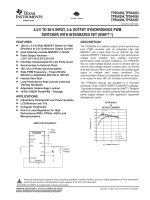
4.5 V TO 20 V INPUT, 3 A OUTPUT SYNCHRONOUS PWM SWITCHER WITH INTEGRATED FET (SWIFT) doc
Bạn đang xem bản rút gọn của tài liệu. Xem và tải ngay bản đầy đủ của tài liệu tại đây (539.02 KB, 28 trang )
TPS54352, TPS54353
TPS54354, TPS54355
TPS54356, TPS54357
SLVS519 − MAY 2004
4.5ĆV TO 20ĆV INPUT, 3ĆA OUTPUT SYNCHRONOUS PWM
SWITCHER WITH INTEGRATED FET (SWIFT)
6,4 mm y 5,0 mm
FEATURES
D 100 mΩ, 4.5-A Peak MOSFET Switch for High
Efficiency at 3-A Continuous Output Current
D Uses External Lowside MOSFET or Diode
D Fixed Output Versions −
1.2V/1.5V/1.8V/2.5V/3.3V/5.0V
D Internally Compensated for Low Parts Count
D Synchronizes to External Clock
D 1805 Out of Phase Synchronization
D Wide PWM Frequency − Fixed 250 kHz,
500 kHz or Adjustable 250 kHz to 700 kHz
D Internal Slow Start
D Load Protected by Peak Current Limit and
Thermal Shutdown
D Adjustable Undervoltage Lockout
D 16-Pin TSSOP PowerPADE Package
APPLICATIONS
D Industrial & Commercial Low Power Systems
D LCD Monitors and TVs
D Computer Peripherals
D Point of Load Regulation for High
Performance DSPs, FPGAs, ASICs and
Microprocessors
PH
VIN
PGND
BOOT
VSENSE
PWRPAD
BIAS
ENA
PWRGD
Input
Voltage
Output
Voltage
LSG
TPS54356
SYNC
SIMPLIFIED SCHEMATIC
DESCRIPTION
The TPS5435x is a medium output current synchronous
buck PWM converter with an integrated high side
MOSFET and a gate driver for an optional low side
external MOSFET. Features include a high performance
voltage error amplifier that enables maximum
performance under transient conditions. The TPS5435x
has an under-voltage-lockout circuit to prevent start-up
until the input voltage reaches a preset value; an internal
slow-start circuit to limit in-rush currents; and a power good
output to indicate valid output conditions. The
synchronization feature is configurable as either an input
or an output for easy 180° out of phase synchronization.
The TPS5435x devices are available in a thermally
enhanced 16-pin TSSOP (PWP) PowerPAD package.
TI provides evaluation modules and the SWIFT Designer
software tool to aid in quickly achieving high-performance
power supply designs to meet aggressive equipment
development cycles.
50
55
60
65
70
75
80
85
90
95
100
01234
V
I
= 12 V
V
O
= 3.3 V
f
s
= 500 kHz
V
I
= 12 V
V
I
= 6 V
I
O
− Output Current − A
Efficiency − %
EFFICIENCY
vs
OUTPUT CURRENT
PRODUCTION DATA information is current as of publication date. Products
conform to specifications per the terms of Texas Instruments standard warranty.
Production processing does not necessarily include testing of all parameters.
Please be aware that an important notice concerning availability, standard warranty, and use in critical applications of Texas Instruments
semiconductor products and disclaimers thereto appears at the end of this data sheet.
www.ti.com
Copyright 2004, Texas Instruments Incorporated
PowerPAD and SWIFT are trademarks of Texas Instruments.
TPS54352, TPS54353
TPS54354, TPS54355
TPS54356, TPS54357
SLVS519 − MAY 2004
www.ti.com
2
These devices have limited built-in ESD protection. The leads should be shorted together or the device placed in conductive foam during
storage or handling to prevent electrostatic damage to the MOS gates.
ORDERING INFORMATION
T
A
OUTPUT VOLTAGE PACKAGE PART NUMBER
1.2 V Plastic HTSSOP (PWP) TPS54352PWP
1.5 V Plastic HTSSOP (PWP) TPS54353PWP
−40°C to 85°C
1.8 V Plastic HTSSOP (PWP) TPS54354PWP
−40
°
C to 85
°
C
2.5 V Plastic HTSSOP (PWP) TPS54355PWP
3.3 V Plastic HTSSOP (PWP) TPS54356PWP
5.0 V Plastic HTSSOP (PWP) TPS54357PWP
(1)
The PWP package is also available taped and reeled. Add an R suffix to the device type (i.e. TPS5435xPWPR).
PACKAGE DISSIPATION RATINGS
(1)
PACKAGE
THERMAL IMPEDANCE
JUNCTION-TO-AMBIENT
T
A
= 25°C
POWER RATING
T
A
= 70°C
POWER RATING
T
A
= 85°C
POWER RATING
16-Pin PWP with solder(2) 42.1°C/W 2.36 1.31 0.95
16-Pin PWP without solder 151.9°C/W 0.66 0.36 0.26
(1)
See Figure 46 for power dissipation curves.
(2)
Test Board Conditions
1. Thickness: 0.062”
2. 3” x 3”
3. 2 oz. Copper traces located on the top and bottom of the PCB for soldering
4. Copper areas located on the top and bottom of the PCB for soldering
5. Power and ground planes, 1 oz. copper (0.036 mm thick)
6. Thermal vias, 0.33 mm diameter, 1.5 mm pitch
7. Thermal isolation of power plane
For more information, refer to TI technical brief SLMA002.
TPS54352, TPS54353
TPS54354, TPS54355
TPS54356, TPS54357
SLVS519 − MAY 2004
www.ti.com
3
ABSOLUTE MAXIMUM RATINGS
over operating free-air temperature range unless otherwise noted
(1)
UNIT
VIN −0.3 V to 21.5 V
VSENSE −0.3 V to 8.0 V
Input voltage range, V
I
UVLO −0.3 V to 8.0 V
Input voltage range, V
I
SYNC −0.3 V to 4.0 V
ENA −0.3 V to 4.0 V
BOOT VI(PH) + 8.0 V
VBIAS −0.3 to 8.5 V
LSG −0.3 to 8.5 V
SYNC −0.3 to 4.0 V
Output voltage range, V
O
RT −0.3 to 4.0 V
Output voltage range, V
O
PWRGD −0.3 to 6.0 V
COMP −0.3 to 4.0 V
PH −1.5 V to 22 V
PH Internally Limited (A)
Source current, I
O
LSG (Steady State Current) 10 mA
Source current, I
O
COMP, VBIAS 3 mA
SYNC 5 mA
LSG (Steady State Current) 100 mA
Sink current, I
S
PH (Steady State Current) 500 mA
Sink current, I
S
COMP 3 mA
ENA, PWRGD 10 mA
Voltage differential AGND to PGND ±0.3 V
Operating virtual junction temperature range, T
J
−40°C to +150°C
Storage temperature, T
stg
−65°C to +150°C
Lead temperature 1,6 mm (1/16 inch) from case for 10 seconds 260°C
(1)
Stresses beyond those listed under “absolute maximum ratings” may cause permanent damage to the device. These are stress ratings only, and
functional operation of the device at these or any other conditions beyond those indicated under “recommended operating conditions” is not
implied. Exposure to absolute-maximum-rated conditions for extended periods may affect device reliability.
ELECTROSTATIC DISCHARGE (ESD) PROTECTION
MIN MAX UNIT
Human body model 600 V
CDM 1.5 kV
RECOMMENDED OPERATING CONDITIONS
MIN NOM MAX UNIT
Input voltage range, V
I
TPS54352−6 4.5 20
V
Input voltage range, V
I
TPS54357 6.65 20
V
Operating junction temperature, T
J
−40 125 °C
TPS54352, TPS54353
TPS54354, TPS54355
TPS54356, TPS54357
SLVS519 − MAY 2004
www.ti.com
4
ELECTRICAL CHARACTERISTICS
T
J
= –40°C to 125°C, VIN = 4.5 V to 20 V (unless otherwise noted)
PARAMETER TEST CONDITIONS MIN TYP MAX UNIT
SUPPLY CURRENT
I
Q
Quiescent current
Operating current, PH pin open,
No external low side MOSFET, RT = Hi-Z
5 mA
I
Q
Quiescent current
Shutdown, ENA = 0 V 1 mA
Start threshold voltage
TPS54352−6 4.32 4.49
V
Start threshold voltage
TPS54357 6.4 6.65
V
VIN
Stop threshold voltage
TPS54352−6 3.69 3.97
V
VIN
Stop threshold voltage
TPS54357 5.45 5.80
V
Hysteresis
TPS54352−6 350 mV
Hysteresis
TPS54357 600 mV
OUTPUT VOLTAGE
TPS54352
T
J
= 25°C, I
O
= 100 mA to 3 A 1.88 1.2 1.212
TPS54352
I
O
= 100 mA to 3 A 1.176 1.2 1.224
TPS54353
T
J
= 25°C, I
O
= 100 mA to 3 A 1.485 1.5 1.515
TPS54353
I
O
= 100 mA to 3 A 1.47 1.5 1.53
TPS54354
T
J
= 25°C, I
O
= 100 mA to 3 A 1.782 1.8 1.818
V
O
Output voltage
TPS54354
I
O
= 100 mA to 3 A 1.764 1.8 1.836
V
V
O
Output voltage
TPS54355
T
J
= 25°C, I
O
= 100 mA to 3 A 2.475 2.5 2.525
V
TPS54355
I
O
= 100 mA to 3 A 2.45 2.5 2.55
TPS54356
T
J
= 25°C, VIN = 5.5 V to 20 V, I
O
= 100 mA to 3 A 3.267 3.3 3.333
TPS54356
VIN = 5.5 V to 20 V, I
O
= 100 mA to 3 A 3.234 3.3 3.366
TPS54357
T
J
= 25°C, VIN = 7.5 V to 20 V, I
O
= 100 mA to 3 A 4.95 5.0 5.05
TPS54357
VIN = 7.5 V to 20 V, I
O
= 100 mA to 3 A 4.90 5.0 5.10
UNDER VOLTAGE LOCK OUT (UVLO PIN)
Start threshold voltage 1.20 1.24 V
UVLO
Stop threshold voltage 1.02 1.10 V
UVLO
Hysteresis 100 mV
BIAS VOLTAGE (VBIAS PIN)
VBIAS
Output voltage
I
VBIAS
= 1 mA, VIN ≥ 12 V 7.5 7.8 8.0
V
VBIAS
Output voltage
I
VBIAS
= 1 mA, VIN = 4.5 V 4.4 4.47 4.5
V
OSCILLATOR (RT PIN)
Internally set PWM switching frequency
RT Grounded 200 250 300
kHz
Internally set PWM switching frequency
RT Open 400 500 600
kHz
Externally set PWM switching frequency RT = 100 kΩ (1% resistor to AGND) 425 500 575 kHz
TPS54352, TPS54353
TPS54354, TPS54355
TPS54356, TPS54357
SLVS519 − MAY 2004
www.ti.com
5
ELECTRICAL CHARACTERISTICS (CONTINUED)
T
J
= –40°C to 125°C, VIN = 4.5 V to 20 V (unless otherwise noted)
PARAMETER TEST CONDITIONS MIN TYP MAX UNIT
FALLING EDGE TRIGGERED BIDIRECTIONAL SYNC SYSTEM (SYNC PIN)
SYNC out low-to-high rise time (10%/90%)
(1)
25 pF to ground
200 500 ns
SYNC out high-to-low fall time (90%/10%)
(1)
25 pF to ground
5 10 ns
Falling edge delay time
(1)
Delay from rising edge to rising edge of PH
pins, see Figure 19
180 °
Minimum input pulse width
(1)
RT = 100 kΩ
100 ns
Delay (falling edge SYNC to rising edge PH)
(1)
RT = 100 kΩ
360 ns
SYNC out high level voltage 50-kΩ Resistor to ground, no pullup resistor
2.5 V
SYNC out low level voltage
0.6 V
SYNC in low level threshold
0.8 V
SYNC in high level threshold
2.3 V
SYNC in frequency range
(1)
Percentage of programmed frequency −10% 10%
SYNC in frequency range
(1)
225 770 kHz
FEED− FORWARD MODULATOR (INTERNAL SIGNAL)
Modulator gain VIN = 12 V, T
J
= 25°C 8 V/V
Modulator gain variation −25% 25%
Minimum controllable ON time
(1)
180 ns
Maximum duty factor
(1)
VIN = 4.5 V 80% 86%
VSENSE PIN
Input bias current, VSENSE pin 1 µA
ENABLE (ENA PIN)
Disable low level input voltage 0.5 V
TPS54352
f
s
= 250 kHz, RT = ground
(1)
3.20
TPS54352
f
s
= 500 kHz, RT = Hi−Z
(1)
1.60
TPS54353
f
s
= 250 kHz, RT = ground
(1)
4.00
TPS54353
f
s
= 500 kHz, RT = Hi−Z
(1)
2.00
TPS54354
f
s
= 250 kHz, RT = ground
(1)
4.60
Internal slow-start time
TPS54354
f
s
= 500 kHz, RT = Hi−Z
(1)
2.30
ms
Internal slow-start time
(10% to 90%)
TPS54355
f
s
= 250 kHz, RT = ground
(1)
4.40
ms
(10% to 90%)
TPS54355
f
s
= 500 kHz, RT = Hi−Z
(1)
2.20
TPS54356
f
s
= 250 kHz, RT = ground
(1)
5.90
TPS54356
f
s
= 500 kHz, RT = Hi−Z
(1)
2.90
TPS54357
f
s
= 250 kHz, RT = ground
(1)
5.40
TPS54357
f
s
= 500 kHz, RT = Hi−Z
(1)
2.70
Pullup current source 1.8 5 10 µA
Pulldown MOSFET I
I(ENA)
= 1 mA 0.1 V
POWER GOOD (PWRGD PIN)
Power good threshold Rising voltage 97%
Rising edge delay
(1)
f
s
= 250 kHz 4
ms
Rising edge delay
(1)
f
s
= 500 kHz 2
ms
Output saturation voltage I
sink
= 1 mA, VIN > 4.5 V 0.05 V
PWRGD
Output saturation voltage I
sink
= 100 µA, VIN = 0 V 0.76 V
PWRGD
Open drain leakage current Voltage on PWRGD = 6 V 3 µA
(1)
Ensured by design, not production tested.
TPS54352, TPS54353
TPS54354, TPS54355
TPS54356, TPS54357
SLVS519 − MAY 2004
www.ti.com
6
ELECTRICAL CHARACTERISTICS (CONTINUED)
T
J
= –40°C to 125°C, VIN = 4.5 V to 20 V (unless otherwise noted)
PARAMETER TEST CONDITIONS MIN TYP MAX UNIT
CURRENT LIMIT
Current limit VIN = 12 V 3.3 4.5 6.5 A
Current limit hiccup time
(1)
f
s
= 500 kHz 4.5 ms
THERMAL SHUTDOWN
Thermal shutdown trip point
(1)
165 _C
Thermal shutdown hysteresis
(1)
7 _C
LOW SIDE MOSFET DRIVER (LSG PIN)
Turn on rise time, (10%/90%)
(1)
VIN = 4.5 V, Capacitive load = 1000 pF
15 ns
Deadtime
(1)
VIN = 12 V
60 ns
Driver ON resistance
VIN = 4.5 V sink/source
7.5
Ω
Driver ON resistance
VIN = 12 V sink/source
5
Ω
OUTPUT POWER MOSFETS (PH PIN)
Phase node voltage when disabled DC conditions and no load, ENA = 0 V
0.5 V
Voltage drop, low side FET and diode
VIN = 4.5 V, Idc = 100 mA
1.13 1.42
V
Voltage drop, low side FET and diode
VIN = 12 V, Idc = 100 mA
1.08 1.38
V
r
DS(ON)
High side power MOSFET switch
(2)
VIN = 4.5 V, BOOT−PH = 4.5 V, I
O
= 0.5 A
150 300
mΩ
r
DS(ON)
High side power MOSFET switch
(2)
VIN = 12 V, BOOT−PH = 8 V, I
O
= 0.5 A
100 200
m
Ω
(1)
Ensured by design, not production tested.
(2)
Resistance from VIN to PH pins.
TPS54352, TPS54353
TPS54354, TPS54355
TPS54356, TPS54357
SLVS519 − MAY 2004
www.ti.com
7
PIN ASSIGNMENTS
1
2
3
4
5
6
7
8
16
15
14
13
12
11
10
9
VIN
VIN
UVLO
PWRGD
RT
SYNC
ENA
COMP
BOOT
PH
PH
LSG
VBIAS
PGND
AGND
VSENSE
PWP PACKAGE
(TOP VIEW)
THERMAL
PAD
NOTE:
If there is not a Pin 1 indicator, turn device to enable
reading the symbol from left to right. Pin 1 is at the lower
left corner of the device.
Terminal Functions
TERMINAL
DESCRIPTION
NO. NAME
DESCRIPTION
1, 2 VIN Input supply voltage, 4.5 V to 20 V. Must bypass with a low ESR 10-µF ceramic capacitor. Place cap as close to device as
possible; see Figure 23 for an example.
3 UVLO Undervoltage lockout pin. Connecting an external resistive voltage divider from VIN to the pin will override the internal
default VIN start and stop thresholds.
4 PWRGD Power good output. Open drain output. A low on the pin indicates that the output is less than the desired output voltage.
There is an internal rising edge filter on the output of the PWRGD comparator.
5 RT Frequency setting pin. Connect a resistor from RT to AGND to set the switching frequency. Connecting the RT pin to
ground or floating will set the frequency to an internally preselected frequency.
6 SYNC Bidirectional synchronization I/O pin. SYNC pin is an output when the RT pin is floating or connected low. The output is a
falling edge signal out of phase with the rising edge of PH. SYNC may be used as an input to synchronize to a system clock
by connecting to a falling edge signal when an RT resistor is used. See 180° Out of Phase Synchronization operation in the
Application Information section. In ALL cases, a 10 kΩ resistor Must be tied to the SYNC pin in parallel with ground. For
information on how to extend slow start, see the Enable (ENA) and Internal Slow Start section on page 9.
7 ENA Enable. Below 0.5 V, the device stops switching. Float pin to enable.
8 COMP Error amplifier output. Do NOT connect ANYTHING to this pin.
9 VSENSE Feedback pin
10 AGND Analog ground—internally connected to the sensitive analog ground circuitry. Connect to PGND and PowerPAD.
11 PGND Power ground—Noisy internal ground—Return currents from the LSG driver output return through the PGND pin. Connect
to AGND and PowerPAD.
12 VBIAS Internal 8.0-V bias voltage. A 1.0-µF ceramic bypass capacitance is required on the VBIAS pin.
13 LSG Gate drive for optional low side MOSFET. Connect gate of n-channel MOSFET for a higher efficiency synchronous buck
converter configuration. Otherwise, leave open and connect schottky diode from ground to PH pins.
14, 15 PH Phase node—Connect to external L−C filter.
16 BOOT Bootstrap capacitor for high side gate driver. Connect a 0.1-µF ceramic capacitor from BOOT to PH pins.
PowerPAD PGND and AGND pins must be connected to the exposed pad for proper operation. See Figure 23 for an example PCB
layout.
TPS54352, TPS54353
TPS54354, TPS54355
TPS54356, TPS54357
SLVS519 − MAY 2004
www.ti.com
8
FUNCTIONAL BLOCK DIAGRAM
VBIAS
PH
BOOT
VIN
LSG
VBIAS
Error
Amplifier
2x Oscillator
PWM Ramp
(FeedFoward)
SYNC
RT
VSENSE
PWM
Comparator
Reference
System
ENA
VBIAS
Hiccup
Timer
Thermal
Shutdown
Current Limit
Hiccup
Hiccup
UVLO
UVLO
UVLO
1.2V
Bias + Drive
Regulator
PWRGD
AGNDPGND
Rising
Edge
Delay
VBIAS
COMP
Adaptive Deadtime
and
Control Logic
97% Ref
POWERPAD
VSENSE
UVLO
S
R
Q
320 kΩ
125 kΩ
(1)
5 µA
(1)
75 kΩ for the TPS54357
Z3
Z1
Z2
Z5
Z4
TPS5435X
DETAILED DESCRIPTION
Undervoltage Lockout (UVLO)
The undervoltage lockout (UVLO) system has an internal
voltage divider from VIN to AGND. The defaults for the
start/stop values are labeled VIN and given in Table 1. The
internal UVLO threshold can be overridden by placing an
external resistor divider from VIN to ground. The internal
divider values are approximately 320 kΩ for the high side
resistor and 125 kΩ for the low side resistor. The divider
ratio (and therefore the default start/stop values) is quite
accurate, but the absolute values of the internal resistors
may vary as much as 15%. If high accuracy is required for
an externally adjusted UVLO threshold, select lower value
external resistors to set the UVLO threshold. Using a 1-kΩ
resistor for the low side resistor (R2 see Figure 1) is
recommended. Under no circumstances should the UVLO
pin be connected directly to VIN.
Table 1. Start/Stop Voltage Threshold
START VOLTAGE THRESHOLD STOP VOLTAGE THRESHOLD
VIN (Default)
TPS54352−6 4.49 3.69
VIN (Default)
TPS54357 6.65 5.45
UVLO 1.24 1.02
The equations for selecting the UVLO resistors are:
R1
VIN(start) 1kW
1.24 V
1kW
VIN(stop)
(R1 1kW) 1.02 V
1kW
(1)
(2)
TPS54352, TPS54353
TPS54354, TPS54355
TPS54356, TPS54357
SLVS519 − MAY 2004
www.ti.com
9
320 kΩ
125 kΩ
(1)
R1
R2
Input
1 kΩ
Voltage
Supply
(1)
75 kΩ for the TPS54357
Figure 1. Circuit Using External UVLO Function
For applications which require an undervoltage lock out
(UVLO) threshold greater than 4.49 V (6.6 V for
TPS54357), external resistors may be implemented, see
Figure 1, to adjust the start voltage threshold. For example,
an application needing an UVLO start voltage of
approximately 7.8 V using the equation (1), R1 is
calculated to the nearest standard resistor value of
5.36 kΩ. Using equation (2), the input voltage stop
threshold is calculated as 6.48 V.
Enable (ENA) and Internal Slow Start
The TPS5435x has an internal digital slow start that ramps
the reference voltage to its final value in 1150 switching
cycles. The internal slow start time (10% − 90%) is
approximated by the following expression:
T
SS_INTERNAL
(ms)
1.15k
ƒ
s
(kHz) n
Use n in Table 2
Table 2. Slow Start Characteristics
DEVICE n
TPS54352 1.485
TPS54353 1.2
TPS54354 1
TPS54355 1.084
TPS54356 0.818
TPS54357 0.900
Once the TPS5435x device is in normal regulation, the
ENA pin is high. If the ENA pin is pulled below the stop
threshold of 0.5 V, switching stops and the internal slow
start resets. If an application requires the TPS5435x to be
disabled, use open drain or open collector output logic to
interface to the ENA pin (see Figure 2). The ENA pin has
an internal pullup current source. Do not use external
pullup resistors.
5 µA
Disabled
Enabled
R
SS
C
SS
Figure 2. Interfacing to the ENA Pin
Extending Slow Start Time
In applications that use large values of output capacitance
there may be a need to extend the slow start time to
prevent the startup current from tripping the current limit.
The current limit circuit is designed to disable the high side
MOSFET and reset the internal voltage reference for a
short amount of time when the high side MOSFET current
exceeds the current limit threshold. If the output
capacitance and load current cause the startup current to
exceed the current limit threshold, the power supply output
will not reach the desired output voltage. To extend the
slow start time and to reduce the startup current, an
external resistor and capacitor can be added to the ENA
pin. The slow start capacitance is calculated using the
following equation:
Use n in Table 2
C
SS
(µF) = 5.55 10
−3
n T
ss
(ms)
The R
SS
resistor must be 2 kΩ and the slow start capacitor
must be less than 0.47 µF.
Switching Frequency (RT)
The TPS5435x has an internal oscillator that operates at
twice the PWM switching frequency. The internal oscillator
frequency is controlled by the RT pin. Grounding the RT
pin sets the PWM switching frequency to a default
frequency of 250 kHz. Floating the RT pin sets the PWM
switching frequency to 500 kHz.
Connecting a resistor from RT to AGND sets the frequency
according to the following equation (also see Figure 30).
RT(kW)
46000
ƒ
s
(kHz) 35.9
The RT pin controls the SYNC pin functions. If the RT pin
is floating or grounded, SYNC is an output. If the switching
frequency has been programmed using a resistor from RT
to AGND, then SYNC functions as an input.
The internal voltage ramp charging current increases
linearly with the set frequency and keeps the feed forward
modulator constant (Km = 8) regardless of the frequency
set point.
(3)
(4)
(5)
TPS54352, TPS54353
TPS54354, TPS54355
TPS54356, TPS54357
SLVS519 − MAY 2004
www.ti.com
10
Table 3.
SWITCHING FREQUENCY SYNC PIN RT PIN
250 kHz, internally set Generates SYNC output signal AGND
500 kHz, internally set Generates SYNC output signal Float
Externally set to 250 kHz to 700 kHz
Terminate to quiet ground
with 10-kΩ resistor.
R = 215 kΩ to 69 kΩ
Externally synchronized frequency Synchronization Signal
Set RT resistor equal to 90% to 110% of external synchronization
frequency.When using a dual setup (see Figure 27 for example),
if the master 35x device RT pin is left floating, use a 110 kΩ
resistor to tie the slave RT pin to ground. Conversely, if the master
35x device RT pin is grounded, use a 237 kΩ resistor to tie the
slave RT pin to ground.
1805 Out of Phase Synchronization (SYNC)
The SYNC pin is configurable as an input or as an output,
per the description in the previous section. When
operating as an input, the SYNC pin is a falling-edge
triggered signal (see Figures 3, 4, and 19). When operating
as an output, the signal’s falling edge is approximately
180° out of phase with the rising edge of the PH pins. Thus,
two TPS5435x devices operating in a system can share an
input capacitor and draw ripple current at twice the
frequency of a single unit.
When operating the two TPS5435x devices 180° out of
phase, the total RMS input current is reduced. Thus
reducing the amount of input capacitance needed and
increasing efficiency.
When synchronizing a TPS5435x to an external signal, the
timing resistor on the RT pin must be set so that the
oscillator is programmed to run at 90% to 110% of the
synchronization frequency.
V
I(SYNC)
V
O(PH)
Figure 3. SYNC Input Waveform
TPS54352, TPS54353
TPS54354, TPS54355
TPS54356, TPS54357
SLVS519 − MAY 2004
www.ti.com
11
Internal Oscillator
V
O(PH)
V
O(SYNC)
Figure 4. SYNC Output Waveform
Power Good (PWRGD)
The VSENSE pin is compared to an internal reference
signal, if the VSENSE is greater than 97% and no other
faults are present, the PWRGD pin presents a high
impedance. A low on the PWRGD pin indicates a fault. The
PWRGD pin has been designed to provide a weak
pull-down and indicates a fault even when the device is
unpowered. If the TPS5435x has power and has any fault
flag set, the TPS5435x indicates the power is not good by
driving the PWRGD pin low. The following events, singly
or in combination, indicate power is not good:
D VSENSE pin out of bounds
D Overcurrent
D Thermal shutdown
D UVLO undervoltage
D Input voltage not present (weak pull-down)
D Slow-starting
D VBIAS voltage is low
Once the PWRGD pin presents a high impedance (i.e.,
power is good), a VSENSE pin out of bounds condition
forces PWRGD pin low (i.e., power is bad) after a time
delay. This time delay is a function of the switching
frequency and is calculated using equation 6:
T
delay
1000
ƒ
s
(kHz)
ms
Bias Voltage (VBIAS)
The VBIAS regulator provides a stable supply for the
internal analog circuits and the low side gate driver. Up to
1 mA of current can be drawn for use in an external
application circuit. The VBIAS pin must have a bypass
capacitor value of 1.0 µF. X7R or X5R grade dielectric
ceramic capacitors are recommended because of their
stable characteristics over temperature.
Bootstrap Voltage (BOOT)
The BOOT capacitor obtains its charge cycle by cycle from
the VBIAS capacitor. A capacitor from the BOOT pin to the
PH pins is required for operation. The bootstrap
connection for the high side driver must have a bypass
capacitor of 0.1 µF.
Error Amplifier
The VSENSE pin is the error amplifier inverting input. The
error amplifier is a true voltage amplifier with 1.5 mA of
drive capability with a minimum of 60 dB of open loop
voltage gain and a unity gain bandwidth of 2 MHz.
Voltage Reference
The voltage reference system produces a precision
reference signal by scaling the output of a temperature
stable bandgap circuit. During production testing, the
bandgap and scaling circuits are trimmed to produce
0.891 V at the output of the error amplifier, with the
amplifier connected as a voltage follower. The trim
procedure improves the regulation, since it cancels offset
errors in the scaling and error amplifier circuits.
PWM Control and Feed Forward
Signals from the error amplifier output, oscillator, and
current limit circuit are processed by the PWM control
logic. Referring to the internal block diagram, the control
logic includes the PWM comparator, PWM latch, and the
adaptive dead-time control logic. During steady-state
operation below the current limit threshold, the PWM
comparator output and oscillator pulse train alternately
reset and set the PWM latch.
(6)
TPS54352, TPS54353
TPS54354, TPS54355
TPS54356, TPS54357
SLVS519 − MAY 2004
www.ti.com
12
Once the PWM latch is reset, the low-side driver and
integrated pull-down MOSFET remain on for a minimum
duration set by the oscillator pulse width. During this
period, the PWM ramp discharges rapidly to the valley
voltage. When the ramp begins to charge back up, the
low-side driver turns off and the high-side FET turns on.
The peak PWM ramp voltage varies inversely with input
voltage to maintain a constant modulator and power stage
gain of 8 V/V.
As the PWM ramp voltage exceeds the error amplifier
output voltage, the PWM comparator resets the latch, thus
turning off the high-side FET and turning on the low-side
FET. The low-side driver remains on until the next
oscillator pulse discharges the PWM ramp.
During transient conditions, the error amplifier output can
be below the PWM ramp valley voltage or above the PWM
peak voltage. If the error amplifier is high, the PWM latch
is never reset and the high-side FET remains on until the
oscillator pulse signals the control logic to turn the
high-side FET off and the internal low-side FET and driver
on. The device operates at its maximum duty cycle until the
output voltage rises to the regulation set point, setting
VSENSE to approximately the same voltage as the
internal voltage reference. If the error amplifier output is
low, the PWM latch is continually reset and the high-side
FET does not turn on. The internal low-side FET and low
side driver remain on until the VSENSE voltage decreases
to a range that allows the PWM comparator to change
states. The TPS5435x is capable of sinking current
through the external low side FET until the output voltage
reaches the regulation set point.
The minimum on time is designed to be 180 ns. During the
internal slow-start interval, the internal reference ramps
from 0 V to 0.891 V. During the initial slow-start interval, the
internal reference voltage is very small resulting in a
couple of skipped pulses because the minimum on time
causes the actual output voltage to be slightly greater than
the preset output voltage until the internal reference ramps
up.
Deadtime Control
Adaptive dead time control prevents shoot through current
from flowing in the integrated high-side MOSFET and the
external low-side MOSFET during the switching
transitions by actively controlling the turn on times of the
drivers. The high-side driver does not turn on until the
voltage at the gate of the low-side MOSFET is below 1 V.
The low-side driver does not turn on until the voltage at the
gate of the high-side MOSFET is below 1 V.
Low Side Gate Driver (LSG)
LSG is the output of the low-side gate driver. The 100-mA
MOSFET driver is capable of providing gate drive for most
popular MOSFETs suitable for this application. Use the
SWIFT Designer Software Tool to find the most
appropriate MOSFET for the application.
Integrated Pulldown MOSFET
The TPS5435x has a diode-MOSFET pair from PH to
PGND. The integrated MOSFET is designed for light−load
continuous-conduction mode operation when only an
external Schottky diode is used. The combination of
devices keeps the inductor current continuous under
conditions where the load current drops below the
inductor’s critical current. Care should be taken in the
selection of inductor in applications using only a low-side
Schottky diode. Since the inductor ripple current flows
through the integrated low-side MOSFET at light loads, the
inductance value should be selected to limit the peak
current to less than 0.3 A during the high-side FET turn off
time. The minimum value of inductance is calculated using
the following equation:
L(H)
VO
1
VO
VI
ƒ
s
0.6
Thermal Shutdown
The device uses the thermal shutdown to turn off the
MOSFET drivers and controller if the junction temperature
exceeds 165°C. The device is restarted automatically
when the junction temperature decreases to 7°C below the
thermal shutdown trip point and starts up under control of
the slow-start circuit.
Overcurrent Protection
Overcurrent protection is implemented by sensing the
drain-to-source voltage across the high-side MOSFET
and compared to a voltage level which represents the
overcurrent threshold limit. If the drain-to-source voltage
exceeds the overcurrent threshold limit for more than
100 ns, the ENA pin is pulled low, the high-side MOSFET
is disabled, and the internal digital slow-start is reset to 0 V.
ENA is held low for approximately the time that is
calculated by the following equation:
T
HICCUP
(ms)
2250
ƒ
s
(kHz)
Once the hiccup time is complete, the ENA pin is released
and the converter initiates the internal slow-start.
(7)
(8)
TPS54352, TPS54353
TPS54354, TPS54355
TPS54356, TPS54357
SLVS519 − MAY 2004
www.ti.com
13
TYPICAL CHARACTERISTICS
Conditions are V
I
= 12 V, V
O
= 3.3 V, f
s
= 500 kHz, I
O
= 3 A, T
A
= 25 °C, unless otherwise noted
Figure 5
−60
−50
−40
−30
−20
−10
0
10
20
30
40
50
60
100 1 k 10 k 100 k 1 M
−180
−150
−120
−90
−60
−30
0
30
60
90
120
150
180
Gain
Phase
f − Frequency − Hz
G − Gain − dB
Phase − Degrees
MEASURED LOOP RESPONSE
See Figure 25
Figure 6
−0.3
−0.2
−0.1
0
0.1
0.2
0.3
0 0.5 1 1.5 2 2.5 3 3.5
V
I
= 18 V
V
I
= 12 V
V
I
= 6 V
LOAD REGULATION
I
O
− Output Current − A
Output Voltage Change − %
See Figure 25
Figure 7
−0.1
−0.08
−0.06
−0.04
−0.02
0
0.02
0.04
0.06
0.08
0.1
468
10 12 14 16 18 20 22
I
O
= 1.5 A
I
O
= 0 A
I
O
= 3 A
Output Voltage Change − %
V
I
− Input Voltage − V
LINE REGULATION
See Figure 25
Figure 8
50
55
60
65
70
75
80
85
90
95
100
01234
V
I
= 18 V
V
I
= 12 V
V
I
= 6 V
I
O
− Output Current − A
Efficiency − %
EFFICIENCY
vs
OUTPUT CURRENT
See Figure 25
Figure 9
V
I(RIPPLE)
= 100 mV/div (ac coupled)
V
(PH)
= 5 V/div
INPUT RIPPLE VOLTAGE
Time − 1 µs/div
Amplitude
See Figure 25
Figure 10
V
O(RIPPLE)
= 10 mV/div (ac coupled)
V
(PH)
= 5 V/div
OUTPUT RIPPLE VOLTAGE
Time − 1 µs/div
Amplitude
See Figure 25
Figure 11
V
(LSG)
= 5 V/div
V
(PH)
= 5 V/div
GATE DRIVE VOLTAGE
Time − 1 µs/div
Amplitude
See Figure 25
Figure 12
V
O
= 50 mV/div (ac coupled)
I
(PH)
= 1 A/div
LOAD TRANSIENT RESPONSE
Time − 200 µs/div
Load Transient Response − mV
See Figure 25
Figure 13
V
I
= 5 V/div
V
O
= 2 V/div
V
(PWRGD)
= 2 V/div
POWER UP
Time − 2 ms/div
Power Up Response − mV
See Figure 25
TPS54352, TPS54353
TPS54354, TPS54355
TPS54356, TPS54357
SLVS519 − MAY 2004
www.ti.com
14
Conditions are V
I
= 12 V, V
O
= 3.3 V, f
s
= 500 kHz, I
O
= 3 A, T
A
= 25 °C, unless otherwise noted
Figure 14
V
I
= 5 V/div
V
O
= 2 V/div
V
(PWRGD)
= 2 V/div
POWER DOWN
Time − 2 ms/div
Power Down Waveforms − V
See Figure 25
Figure 15
50
55
60
65
70
75
80
85
90
95
100
01234
V
I
= 18 V
I
O
− Output Current − A
Efficiency − %
EFFICIENCY
vs
OUTPUT CURRENT
V
I
= 12 V
V
I
= 6 V
See Figure 26
Figure 16
I
(L1)
= 200 mA/div
V
(PH)
= 5 V/div
CONTINUOUS CONDUCTION MODE
Time − 1 µs/div
Continuous Conduction Mode
See Figure 26
Figure 17
I
(L1)
= 200 mA/div
V
(PH)
= 5 V/div
LIGHT LOAD CONDUCTION
Time − 1 µs/div
Light Load Conduction
See Figure 26
Figure 18
V
I
= 10 V/div
V
O1(3.3)
= 2 V/div
V
(PWRGD1)
= 2 V/div
SEQUENCING WAVEFORMS
Time − 2 ms/div
Sequencing Waveforms − V
V
O2
(1.8)
= 2 V/div
See Figure 27
Figure 19
V
(PH1)
= 10 V/div
V
I
= 50 mV/div (ac coupled)
INPUT RIPPLE CANCELLATION
Time − 1 µs/div
Input Ripple Cancellation − V
V
(PH2)
= 10 V/div
See Figure 27
Figure 20
−60
−50
−40
−30
−20
−10
0
10
20
30
40
50
60
100 1 k 10 k 100 k 1 M
−180
−150
−120
−90
−60
−30
0
30
60
90
120
150
180
Phase
Gain
f − Frequency − Hz
G − Gain − dB
Phase − Degrees
MEASURED LOOP RESPONSE
100 mF POSCAP
See Figure 28
Figure 21
−60
−50
−40
−30
−20
−10
0
10
20
30
40
50
60
100 1 k 10 k 100 k 1 M
−180
−150
−120
−90
−60
−30
0
30
60
90
120
150
180
Phase
Gain
f − Frequency − Hz
G − Gain − dB
Phase − Degrees
MEASURED LOOP RESPONSE
2 x 180 mF SP CAPACITORS
See Figure 29
Figure 22
−60
−50
−40
−30
−20
−10
0
10
20
30
40
50
60
100 1 k 10 k 100 k 1 M
−180
−150
−120
−90
−60
−30
0
30
60
90
120
150
180
Phase
Gain
f − Frequency − Hz
G − Gain − dB
Phase − Degrees
MEASURED LOOP RESPONSE
330 mF OSCON
See Figure 30
TPS54352, TPS54353
TPS54354, TPS54355
TPS54356, TPS54357
SLVS519 − MAY 2004
www.ti.com
15
LAYOUT INFORMATION
Figure 23. TPS5435x PCB Layout
PCB LAYOUT
The VIN pins should be connected together on the printed
circuit board (PCB) and bypassed with a low ESR ceramic
bypass capacitor. Care should be taken to minimize the
loop area formed by the bypass capacitor connections, the
VIN pins, and the TPS5435x ground pins. The minimum
recommended bypass capacitance is 10-µF ceramic with
a X5R or X7R dielectric and the optimum placement is
closest to the VIN pins and the AGND and PGND pins. See
Figure 23 for an example of a board layout. The AGND and
PGND pins should be tied to the PCB ground plane at the
pins of the IC. The source of the low-side MOSFET and the
anode of the Schottky diode should be connected directly
to the PCB ground plane. The PH pins should be tied
together and routed to the drain of the low-side MOSFET
or to the cathode of the external Schottky diode. Since the
PH connection is the switching node, the MOSFET (or
diode) should be located very close to the PH pins, and the
area of the PCB conductor minimized to prevent excessive
capacitive coupling. The recommended conductor width
from pins 14 and 15 is 0.050 inch to 0.075 inch of 1-ounce
copper. The length of the copper land pattern should be no
more than 0.2 inch.
For operation at full rated load, the analog ground plane
must provide adequate heat dissipating area. A 3-inch by
3-inch plane of copper is recommended, though not
mandatory, dependent on ambient temperature and
airflow. Most applications have larger areas of internal
ground plane available, and the PowerPAD should be
connected to the largest area available. Additional areas
on the bottom or top layers also help dissipate heat, and
any area available should be used when 3 A or greater
operation is desired. Connection from the exposed area of
the PowerPAD to the analog ground plane layer should be
made using 0.013-inch diameter vias to avoid solder
wicking through the vias. Four vias should be in the
PowerPAD area with four additional vias outside the pad
area and underneath the package. Additional vias beyond
those recommended to enhance thermal performance
should be included in areas not under the device package.
TPS54352, TPS54353
TPS54354, TPS54355
TPS54356, TPS54357
SLVS519 − MAY 2004
www.ti.com
16
0.1942
0.0150
0.06
0.0256
0.1700
0.1340
0.0690
0.0400
0.0400
0.0400
Minimum recommended exposed copper
area for powerpad. 5mil stencils may
require 10 percent larger area.
Connect Pin 10 AGND
and Pin 11 PGND to
Analog Ground plane in
this area for optimum
performance.
Minimum recommended top
side Analog Ground area.
0.0400
Minimum recommended thermal vias: 4 x
.013 dia. inside powerpad area and
4 x .013 dia. under device as shown.
Additional .018 dia. vias may be used if top
side Analog Ground area is extended.
0.0570
j
0.0130
8 PL
0.1970
0.0371
Figure 24. Thermal Considerations for PowerPAD Layout
TPS54352, TPS54353
TPS54354, TPS54355
TPS54356, TPS54357
SLVS519 − MAY 2004
www.ti.com
17
APPLICATION INFORMATION
+
+
Figure 25. Application Circuit, 12 V to 3.3 V
Figure 25 shows the schematic for a typical TPS54356
application. The TPS54356 can provide up to 3-A output
current at a nominal output voltage of 3.3 V. For proper
thermal performance, the exposed PowerPAD underneath
the device must be soldered down to the printed circuit
board.
DESIGN PROCEDURE
The following design procedure can be used to select
component values for the TPS54356. Alternately, the
SWIFT Designer Software may be used to generate a
complete design. The SWIFT Designer Software uses an
iterative design procedure and accesses a comprehensive
database of components when generating a design. This
section presents a simplified discussion of the design
process.
To begin the design process a few parameters must be
decided upon. The designer needs to know the following:
D Input voltage range
D Output voltage
D Input ripple voltage
D Output ripple voltage
D Output current rating
D Operating frequency
For this design example, use the following as the input
parameters:
DESIGN PARAMETER EXAMPLE VALUE
Input voltage range 6 V to 18 V
Output voltage 3.3 V
Input ripple voltage 300 mV
Output ripple voltage 10 mV
Output current rating 3 A
Operating frequency 500 kHz
SWITCHING FREQUENCY
The switching frequency is set using the RT pin.
Grounding the RT pin sets the PWM switching frequency
to a default frequency of 250 kHz. Floating the RT pin sets
the PWM switching frequency to 500 kHz. By connecting
a resistor from RT to AGND, any frequency in the range of
250 kHz to 700 kHz can be set. Use equation 9 to
determine the proper value of RT.
RT(kW)
46000
ƒ
s
(kHz) 35.9
In this example circuit, RT is not connected and the
switching frequency is set at 500 kHz.
(9)
TPS54352, TPS54353
TPS54354, TPS54355
TPS54356, TPS54357
SLVS519 − MAY 2004
www.ti.com
18
INPUT CAPACITORS
The TPS54356 requires an input decoupling capacitor
and, depending on the application, a bulk input capacitor.
The minimum value for the decoupling capacitor, C9, is
10µF. A high quality ceramic type X5R or X7R is
recommended. The voltage rating should be greater than
the maximum input voltage. Additionally some bulk
capacitance may be needed, especially if the TPS54356
circuit is not located within about 2 inches from the input
voltage source. The value for this capacitor is not critical
but it also should be rated to handle the maximum input
voltage including ripple voltage and should filter the output
so that input ripple voltage is acceptable.
This input ripple voltage can be approximated by equation
10:
DV
IN
I
OUT(MAX)
0.25
C
BULK
ƒ
sw
I
OUT(MAX)
ESR
(MAX)
Where I
OUT(MAX)
is the maximum load current, ƒ
SW
is the
switching frequency, C
BULK
is the bulk capacitor value and
ESR
MAX
is the maximum series resistance of the bulk
capacitor.
The maximum RMS ripple current also needs to be
checked. For worst case conditions, this can be
approximated by equation 11:
I
CIN
I
OUT(MAX)
2
In this case the input ripple voltage would be 140 mV and
the RMS ripple current would be 1.5 A. The maximum
voltage across the input capacitors would be VIN max plus
delta VIN/2. The chosen bulk and bypass capacitors are
each rated for 25 V and the combined ripple current
capacity is greater than 3 A, both providing ample margin.
It is very important that the maximum ratings for voltage
and current are not exceeded under any circumstance.
OUTPUT FILTER COMPONENTS
Inductor Selection
To calculate the minimum value of the output inductor, use
equation 12:
L
(MIN)
V
OUT
V
IN(MAX)
V
OUT
V
IN(MAX)
K
IND
I
OUT
ƒ
sw
K
IND
is a coefficient that represents the amount of inductor
ripple current relative to the maximum output current. For
designs using low ESR output capacitors such as
ceramics, use K
IND
= 0.3. When using higher ESR output
capacitors, K
IND
= 0.2 yields better results.
For this design example use K
IND
= 0.1 to keep the
inductor ripple current small. The minimum inductor value
is calculated to be 17.96 µH. The next highest standard
value is 22 µH, which is used in this design.
For the output filter inductor it is important that the RMS
current and saturation current ratings not be exceeded.
The RMS inductor current can be found from equation 13:
I
L(RMS)
I
2
OUT(MAX)
1
12
V
OUT
V
IN(MAX)
V
OUT
V
IN(MAX)
L
OUT
ƒ
sw
0.8
2
(13)
and the peak inductor current can be determined with
equation 14:
(1
4)
I
L(PK)
I
OUT(MAX)
V
OUT
V
IN(MAX)
V
OUT
1.6 V
IN(MAX)
L
OUT
ƒ
sw
For this design, the RMS inductor current is 3.007 A and
the peak inductor current is 3.15 A. The chosen inductor
is a Coiltronics DR127−220 22 µH. It has a saturation
current rating of 7.57 A and a RMS current rating of 4 A,
easily meeting these requirements. A lesser rated inductor
could be used if less margin is desired. In general, inductor
values for use with the TPS54356 are in the range of 6.8
µH to 47 µH.
Capacitor Requirements
The important design factors for the output capacitor are
dc voltage rating, ripple current rating, and equivalent
series resistance (ESR). The dc voltage and ripple current
ratings cannot be exceeded. The ESR is important
because along with the inductor current it determines the
amount of output ripple voltage. The actual value of the
output capacitor is not critical, but some practical limits do
exist.
Consider the relationship between the desired closed loop
crossover frequency of the design and LC corner
frequency of the output filter. In general, it is desirable to
keep the closed loop crossover frequency at less than 1/5
of the switching frequency. With high switching
frequencies such as the 500-kHz frequency of this design,
internal circuit limitations of the TPS54356 limit the
practical maximum crossover frequency to about 70 kHz.
Additionally, the capacitor type and value must be chosen
to work with the internal compensation network of the
TPS5435x family of dc/dc converters. To allow for
adequate phase gain in the compensation network, the LC
corner frequency should be about one decade or so below
the closed loop crossover frequency. This limits the
minimum capacitor value for the output filter to:
C
OUT(MIN)
1
L
OUT
(
K
2pƒ
CO
)
2
(10)
(11)
(12)
(15)
TPS54352, TPS54353
TPS54354, TPS54355
TPS54356, TPS54357
SLVS519 − MAY 2004
www.ti.com
19
Where K is the frequency multiplier for the spread between
f
LC
and f
CO
. K should be between 5 and 15, typically 10 for
one decade difference. For a desired crossover of 20 kHz
and a 22-µH inductor, the minimum value for the output
capacitor is 288 µF. The selected output capacitor must be
rated for a voltage greater than the desired output voltage
plus one half the ripple voltage. Any derating amount must
also be included. The maximum RMS ripple current in the
output capacitor is given by equation 16:
I
COUT(RMS)
1
12
V
OUT
V
IN(MAX)
V
OUT
V
IN(MAX)
L
OUT
ƒ
sw
(16)
The calculated RMS ripple current is 156 mA in the
output capacitors.
CHOOSING CAPACITOR VALUE
For this design example, a relatively large aluminum
electrolytic capacitor is combined with a smaller value
ceramic capacitor. This combination provides a stable high
performance design at a relatively low cost. Also, by
carefully choosing the capacitor values and ESRs, the
design can be tailored to complement the internal
compensation poles and zeros of the TPS54356.
These preconfigured poles and zeroes internal to the
TPS54356 limit the range of output filter configurations. A
variety of capacitor values and types of dielectric are
supported. There are a number of different ways to
calculate the output filter capacitor value and ESR to work
with the internal compensation network. This procedure
outlines a relatively simple procedure that produces good
results with an output filter consisting of a high ESR
dielectric capacitor in parallel with a low ESR ceramic
capacitor. Use of the SWIFT Designer Software for
designs with unusually high closed loop crossover
frequencies, low value, low ESR output capacitors such as
ceramics or if the designer is unsure about the design
procedure.
The TPS54356 contains a compensation network with the
following nominal characteristics:
ƒ
INT
1.7 kHZ
ƒ
Z1
2.5 kHZ
ƒ
Z2
4.8 kHZ
ƒ
P1
95 kHZ
ƒ
P2
125 kHZ
For a stable design, the closed loop crossover frequency
should be set less than one fifth of the switching frequency,
and the phase margin at crossover must be greater than
45 degrees. The general procedure outlined here
produces results consistent with these requirements
without going into great detail about the theory of loop
compensation.
In this case, the output filter LC corner frequency should be
selected to be near the first compensation zero frequency
as described by equation 17:
ƒ
LC
1
2p L
OUT
C2
ƒ
Z1
Placement of the LC corner frequency at f
Z1
is not critical,
it only needs to be close. For the design example, f
LC
= 2
kHz.
Solving for C2 using equation 18:
C2
1
4p
2
ƒ
2
Z1
L
OUT
The desired value for C2 is calculated as 184 µF. A close
standard value of 330 µF is chosen with a resulting LC
corner frequency of 1.9 kHz. As to be shown, this value is
not critical as long as it results in a corner frequency in the
vicinity of f
Z1
.
Next, when using a large ceramic capacitor in parallel with
a high ESR electrolytic capacitor, there is a pole in the
output filter that should be at f
Z2
as shown in equation 19:
ƒ
P(ESR)
1
2pR
(C2ESR)
C5
ƒ
Z2
Now the actual C2 capacitor must be selected based on
the ESR and the value of capacitor C5 so that the above
equation is satisfied. In this example, the R
(C2ESR)
C5
product should be 3.18 10
−5
. From the available
capacitors, by choosing a Panasonic EEVFKOJ331XP
aluminum electrolytic capacitor with a nominal ESR of
0.34 Ω yields a calculated value for C5 of 98 µF. The
closest standard value is 100 µF. As the actual ESR of the
capacitor can vary by a large amount, this value also is not
critical.
The closed loop crossover frequency should be greater
than f
LC
and less than one fifth of the switching frequency.
Also, the crossover frequency should not exceed 70 kHz,
as the error amplifier may not provide the desired gain. As
stated previously, closed loop crossover frequencies
between 5 and 15 times f
LC
work well. For this design, the
crossover frequency can be estimated by:
ƒ
CO
1.125 10
3
ƒ
P(ESR)
ƒ
LC
This simplified equation is valid for this design because the
output filter capacitors are mixed technology. Compare
this result to the actual measured loop response plot of
(17)
(18)
(19)
(20)
TPS54352, TPS54353
TPS54354, TPS54355
TPS54356, TPS54357
SLVS519 − MAY 2004
www.ti.com
20
Figure 5. The measured closed loop crossover frequency
of 19.95 kHz differs from the calculated value because the
actual output filter capacitor component parameters
differed slightly from the specified data sheet values.
CAPACITOR ESR AND OUTPUT RIPPLE
The amount of output ripple voltage as specified in the
initial design parameters is determined by the
maximum ESR of the output capacitor and the input
ripple current. The output ripple voltage is the inductor
ripple current times the ESR of the output filter so the
maximum specified ESR as listed in the capacitor data
sheet is given by equation 21:
ESR
(MAX)
V
IN(MAX)
L
OUT
ƒ
sw
0.8
V
OUT
V
IN(MAX)
V
OUT
DV
pp(MAX)
and the maximum ESR required is 33 mΩ. In this design,
the aluminum electrolytic capacitor has an ESR of 0.340
mΩ, but it is in parallel with an ultra low ESR ceramic
capacitor of 2 mΩ maximum. The measured output ripple
voltage for this design is approximately 4 mV
p−p
as shown
in Figure 10.
BIAS AND BOOTSTRAP CAPACITORS
Every TPS54356 design requires a bootstrap capacitor,
C3 and a bias capacitor, C4. The bootstrap capacitor must
be 0.1 µF. The bootstrap capacitor is located between the
PH pins and BOOT pin. The bias capacitor is connected
between the VBIAS pin and AGND. The value should be
1.0 µF. Both capacitors should be high quality ceramic
types with X7R or X5R grade dielectric for temperature
stability. They should be placed as close to the device
connection pins as possible.
LOW-SIDE FET
The TPS54356 is designed to operate using an external
low-side FET, and the LSG pin provides the gate drive
output. Connect the drain to the PH pin, the source to
PGND, and the gate to LSG. The TPS54356 gate drive
circuitry is designed to accommodate most common
n-channel FETs that are suitable for this application. The
SWIFT Designer Software can be used to calculate all the
design parameters for low-side FET selection. There are
some simplified guidelines that can be applied that
produce an acceptable solution in most designs.
The selected FET must meet the absolute maximum
ratings for the application:
D Drain-source voltage (V
DSS
) must be higher
than the maximum voltage at the PH pin,
which is V
INMAX
+ 0.5 V.
D Gate-source voltage (V
GSS
) must be greater
than 8 V.
D Drain current (
ld
) must be greater than 1.1 x
I
OUTMAX
.
D Drain-source on resistance (R
DSON
) should be
as small as possible, less than 30 mW is
desirable. Lower values for R
DSON
result in
designs with higher efficiencies. It is
important to note that the low-side FET on
time is typically longer than the high-side
FET on time, so attention paid to low-side
FET parameters can make a marked
improvement in overall efficiency.
D Total gate charge (Q
g
) must be less than 50
nC. Again, lower Q
g
characteristics result in
higher efficiencies.
D Additionally, check that the device chosen is
capable of dissipating the power losses.
For this design, a Fairchild FDR6674A 30-V n-channel
MOSFET is used as the low-side FET. This particular FET
is specifically designed to be used as a low-side
synchronous rectifier.
POWER GOOD
The TPS54356 is provided with a power good output pin
PWRGD. This output is an open drain output and is
intended to be pulled up to a 3.3-V or 5-V logic supply. A
10-kΩ, pull-up resistor works well in this application. The
absolute maximum voltage is 6 V, so care must be taken
not to connect this pull-up resistor to VIN if the maximum
input voltage exceeds 6 V.
SNUBBER CIRCUIT
R10 and C11 of the application schematic in Figure 25
comprise a snubber circuit. The snubber is included to
reduce over-shoot and ringing on the phase node when the
internal high-side FET turns on. Since the frequency and
amplitude of the ringing depends to a large degree on
parasitic effects, it is best to choose these component
values based on actual measurements of any design
layout. See literature number SLVP100 for more detailed
information on snubber design.
(21)
TPS54352, TPS54353
TPS54354, TPS54355
TPS54356, TPS54357
SLVS519 − MAY 2004
www.ti.com
21
+
+
Figure 26. 3.3-V Power Supply With Schottky Diode
Figure 26 shows an application where a clamp diode is
used in place of the low-side FET. The TPS54352−7
incorporates an integrated pull-down FET so that the
circuit remains operating in continuous mode during light
load operation. A 3-A, 40-V Schottky diode such as the
Motorola MBRS340T3 or equivalent is recommended.
See Figures 15−17 for efficiency data and switching
waveforms for this circuit.
+
+
+
+
Figure 27. 3.3-V/1.8-V Power Supply with Sequencing
TPS54352, TPS54353
TPS54354, TPS54355
TPS54356, TPS54357
SLVS519 − MAY 2004
www.ti.com
22
Figure 27 is an example of power supply sequencing using
a TPS54356 (U1) to generate an output of 3.3 V, and a
TPS54354 (U2) to generate a 1.8-V output. These output
voltages are typical I/O and core voltages for
microprocessors and FPGAs. In the circuit, the 3.3-V
supply is designed to power up first.
The PWRGD pin of U1 is tied to the ENA pin of U2 so that
the 1.8-V supply starts to ramp up after the 3.3-V supply is
within regulation. Figure 18 shows these start up
sequence waveforms.
Since the RT pin of U1 is floating, the SYNC pin is an
output. This synchronization signal is fed the SYNC pin of
U2. The RT pin of U2 has a 110-kΩ resistor to ground, and
the SYNC pin for this device acts as an input. The 1.8-V
supply operates synchronously with the 3.3-V supply and
their switching node rising edges are approximately 180
degrees out of phase allowing for a reduction in the input
voltage ripple. See Figure 19 for this wave form.
ALTERNATE OUTPUT FILTER DESIGNS
The previous design procedure example demonstrated a
technique to design a 3.3-V power supply using both
aluminum electrolytic and ceramic output filter capacitors.
Other types of output filter capacitors are supported by the
TPS5435x family of dc/dc converters. Figures 26−28 show
designs using other popular capacitor types.
In Figure 28, the TPS54356 shown with a single 100-µF
6-V POSCAP as the output filter capacitor. C10 is a high
frequency bypass capacitor and does not enter into the
design equations. The design procedure is similar to the
previous example except in the design of the output filter.
In the previous example, the output filter LC corner was set
at the first zero in the compensation network, while the
second compensation zero was used to counteract the
output filter pole caused by the interaction of the C2
capacitor ESR with C5. In this design example, the output
LC corner frequency is to be set at the second zero
frequency f
Z2
of the internal compensation network,
approximately 5 kHz, while the first zero is used to provide
phase boost prior to the LC corner frequency.
+
+
Figure 28. 3.3-V Power Supply with Sanyo POSCAP Output Filter Capacitor
Inductor Selection
Using equation 12 and a K
IND
of 0.2, the minimum inductor
value required is 8.98 µH. The closest standard value, 10
µH is selected. RMS and peak inductor currents are the
same as calculated previously.
Capacitor Selection
With the inductor set at 10 µH and a desired corner
frequency of 5 kHz, the output capacitor value is given by:
C
2
1
4p
2
ƒ
Z2
2
L
out
1
4 p
2
5000
2
10
5
101 m
F
Use 100 µF as the closest standard value.
Calculating the RMS ripple current in the output capacitor
using equation 16 yields 156 mA. The POSCAP
6TPC100M capacitor selected is rated for 1700 mA. See
the closed loop response curve for this design in Figure 20.
TPS54352, TPS54353
TPS54354, TPS54355
TPS54356, TPS54357
SLVS519 − MAY 2004
www.ti.com
23
+
+ +
Figure 29. 3.3-V Power Supply with Panasonic SP Output Filter Capacitors
In Figure 29, the TPS54356 shown with two 180-µF 4-V
special polymer dielectric output filter capacitors(C2 and
C5). C10 is a high frequency bypass capacitor and does
not enter into the design equations. In the previous
example, the output LC corner frequency is to be set at the
second zero frequency f
Z2
of the internal compensation
network, approximately 5 kHz, while the first zero is used
to provide phase boost prior to the LC corner frequency.
The special polymer electrolytic capacitors used in this
design require that the closed loop crossover frequency be
lowered due to the significantly lower ESR of this type of
capacitor.
Inductor Selection
The inductor is the same 10-µH value as the previous
example.
Capacitor Selection
To lower the closed loop crossover it is necessary to
reduce the LC corner frequency below 5 kHz. Using a
target value of 2500 Hz, the output capacitor value is given
by:
C
2
1
4p
2
ƒ
Z2
2
L
out
1
4 p
2
2500
2
10
5
405 m
F
Use 2 x 180 µF = 360 µF as a combination of standard
values that is close to 405 µF.
The RMS ripple current in the output capacitor is the same
as before. The selected capacitors are each 3.3 A. See the
closed loop response curve for this design in Figure 21.
+
+
Figure 30. 3.3-V Power Supply with Sanyo OSCON Output Filter Capacitor
In Figure 30, the TPS54356 shown with a Sanyo OSCON
output filter capacitor(C2). C10 is a high frequency bypass
capacitor and does not enter into the design equations.
This design is identical to the previous example except that
a single OSCON capacitor of 330 µF is used for the
calculated value of 405 µF. Compare the closed loop
response for this design in Figure 22 to the closed loop
response in Figure 21. Note that there is only a slight
difference in the response and the general similarity in both
the gain and phase plots. This is the expected result for
these two similar output filters.
Many other additional output filter designs are possible.
Use the SWIFT Designer Software to generate other
designs or follow the general design procedures illustrated
in this application section.
TPS54352, TPS54353
TPS54354, TPS54355
TPS54356, TPS54357
SLVS519 − MAY 2004
www.ti.com
24
Figure 31
200
300
400
500
600
700
800
4 6 8 101214161820
MAXIMUM SWITCHING FREQUENCY
vs
INPUT VOLTAGE
Maximum Switching Frequency − kHz
V
I
− Input Voltage − V
V
O
= 2.5 V
V
O
= 1.2 V
V
O
= 1.5 V
V
O
= 1.8 V
Figure 32
50
75
100
125
150
175
200
225
200 300 400 500 600 700
RT RESISTANCE
vs
SWITCHING FREQUENCY
RT Resistance − kW
Switching Frequency − kHz
Figure 33
3.5
4.0
4.5
5.0
5.5
6.0
6.5
−50 −25 0 25 50 75 100 125 150
VIN(UVLO) START AND STOP
vs
FREE-AIR TEMPERATURE
V
I
− Input Voltage − V
T
A
− Free-Air Temperature − 5C
Start
Start
Stop
Stop
TPS54357
TPS54352−6
Figure 34
3
4
5
6
7
8
9
10
0 5 10 15 20 25
ENABLED SUPPLY CURRENT
vs
INPUT VOLTAGE
Enabled Supply Current − mA
V
I
− Input Voltage − V
T
J
= 25°C
f
S
= 500 kHz
Figure 35
0.9
1.0
1.1
1.2
1.3
0 5 10 15 20 25
DISABLED SUPPLY CURRENT
vs
INPUT VOLTAGE
Disabled Supply Current − mA
V
I
− Input Voltage − V
T
J
= 25°C
Figure 36
4.0
4.5
5.0
5.5
6.0
6.5
7.0
7.5
8.0
0 5 10 15 20 25
BIAS VOLTAGE
vs
INPUT VOLTAGE
V
BIAS
− Bias Voltage − V
V
I
− Input Voltage − V
T
J
= 25°C
Figure 37
96.0
96.5
97.0
97.5
98.0
−50 −25 0 25 50 75 100 125 150
POWER GOOD THRESHOLD
vs
JUNCTION TEMPERATURE
PWRGD − Power Good Threshold − %
T
J
− Junction Temperature − 5C
Figure 38
0.8912
0.8910
0.8908
0.8906
0.8904
0.8902
0.8900
0.8898
−50 −25 0 25 50 75 100 125 150
INTERNAL VOLTAGE REFERENCE
vs
JUNCTION TEMPERATURE
V
ref
− Internal Voltage Reference − V
T
J
− Junction Temperature − 5C
VIN = 12 V
4.0
4.5
5.0
5.5
6.0
5.0 7.5 10.0 12.5 15.0 17.5 20.0
CURRENT LIMIT
vs
INPUT VOLTAGE
Current Limit − A
V
I
− Input Voltage − V
T
J
= 25°C
Figure 39
TPS54352, TPS54353
TPS54354, TPS54355
TPS54356, TPS54357
SLVS519 − MAY 2004
www.ti.com
25
Figure 40
50
70
90
110
130
150
−50 −25 0 25 50 75 100 125 150
ON RESISTANCE
vs
JUNCTION TEMPERATURE
On Resistance − mW
T
J
− Junction Temperature − 5C
V
I
= 12 V
I
O
= 0.5 A
Figure 41
1
1.25
1.50
1.75
2
100 150 200 250 300
PH Voltage − V
PH VOLTAGE
vs
SINK CURRENT
I
CC
− Sink Current − mA
V
I
= 4.5 V
V
I
= 12 V
Figure 42
0
0.05
0.10
0.15
0.20
0.25
0.30
0.35
0.40
0.45
0.50
0 1020304050607080
t − Time − ms
Slow Start Capacitance −
SLOW START CAPACITANCE
vs
TIME
Fµ
R
SS
= 2 kΩ
Figure 43
0
0.5
1
1.5
2
2.5
3
3.5
4
4.5
250 350 450 550 650 750
Switching Frequency − kHz
Power Good Delay − ms
POWER GOOD DELAY
vs
SWITCHING FREQUENCY
Figure 44
2
3
4
5
6
7
8
9
10
250 350 450 550 650 750
Hiccup Time − ms
HICCUP TIME
vs
SWITCHING FREQUENCY
Switching Frequency − kHz
Figure 45
Switching Frequency − kHz
1
1.5
2
2.5
3
3.5
4
4.5
5
250 350 450 550 650 750
Slow Start Time − ms
INTERNAL SLOW START TIME
vs
SWITCHING FREQUENCY
TPS54354
Figure 46
0
20
40
60
80
100
120
140
0 0.5 1 1.5 2 2.5 3 3.5
T
J
= 125°C
− Free-Air Temperature −
FREE-AIR TEMPERATURE
vs
MAXIMUM OUTPUT CURRENT
I
O
− Output Current − A
C
°
T
A
Figure 47
0
2
4
6
0 5 10 15 20 25
MAXIMUM OUTPUT VOLTAGE
vs
INPUT VOLTAGE
− Output Voltage − V
V
O
V
I
− Input Voltage − V
TPS54357
5
3
1
TPS54352
TPS54356
TPS54355
TPS54354
TPS54353
Figure 48
0
0.5
1
1.5
2
2.5
25 45 65 85 105 125
POWER DISSIPATION
vs
FREE-AIR TEMPERATURE
T
A
− Free-Air Temperature − °C
− Power Dissipation − W
P
D
θ
JA
= 42.1°C/W
θ
JA
= 191.9°C/W