Điện tử học : NỐI PN part 7 pps
Bạn đang xem bản rút gọn của tài liệu. Xem và tải ngay bản đầy đủ của tài liệu tại đây (368.75 KB, 5 trang )
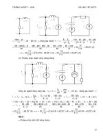
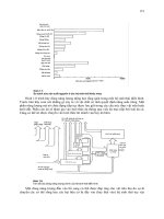
V
I
V
br
Fig.6.15: Reverse I-V characteristics of a pn junction.
From Principles of Electronic Materials and Devices, Second Edition, S.O. Kasap (© McGraw-Hill, 2002)
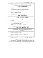
Figure 1.31
AC circuit analysis: (a) circuit with combined dc and sinusoidal input voltages, (b) sinusoidal
diode current superimposed on the quiescent current, (c) sinusoidal diode voltage
superimposed on the quiescent value, and (d) forward-biased diode I-V characteristics with a
sinusoidal current and voltage superimposed on the quiescent values
Figure 1.25
The diode and load line characteristics for the circuit shown in
Figure 1.24
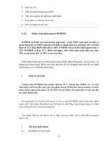
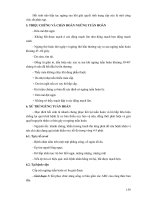
3.ẹieọn trụỷ noỏi pn I
D
a.ẹieọn trụỷ túnh
I
D
Q
0 V
D
V
b.ẹieọn trụỷ ủoọng:
D
D
D
Q
V
R
I
D D
d
D D
Q Q
V d V
r
I d I
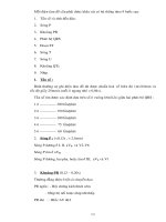
Current
Voltage
0
I
0.5
V
dV
r
d
1
dI
dV
=
dI
I
+
dI
V
+
dV
Tangent
From Principles of Electronic Materials and Devices, Second Edition, S.O. Kasap (© McGraw-Hill, 2002)
Fig. 6.14: The dynamic resistance of the diode is defined as dV/dI
which is the inverse of the tangent at I.