Antennas with Non-Foster Matching Networks phần 4 docx
Bạn đang xem bản rút gọn của tài liệu. Xem và tải ngay bản đầy đủ của tài liệu tại đây (956.17 KB, 12 trang )
P1: RVM
MOBK060-01 MOBK060-Aberle.cls January 19, 2007 17:23
26 ANTENNAS WITH NON-FOSTER MATCHING NETWORKS
2.09 V
-456 uV
-
-193 uV
+
-2.05 mV
-5 V
V-
5 V
V+
5 V
V+
-5 V
V-
2
.
0
9
n
A
R
R1
R
=1 GOhm
1.53 mA
V_ D C
SRC3
Vd c = -5 V
-1.56 mA
V_ DC
SRC4
Vd c =5 V
Port
P2
Num=2
0 A
C
C8
C=0.1 uF
0 A
C
C7
C=0.1 uF
0 A
C
C9
C=0.1 uF
Port
P3
Num=3
Port
P1
Num=1
-2.09 nA
-
3
.
5
7
u
A
-
3
.
3
3
u
A
13.8 uA
1.56 mA
-1.53 mA
opa690
OPA1
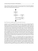
FIGURE26: Schematic of OPA690 for simulation in AgilentADSobtained by using the SPICE model
and the data sheet for the device provided by TI
performance of several of these NIC circuits. Unfortunately, successful simulation of an NIC
circuit has not always led us to a successful physical implementation. One reason for this is that
all NIC circuits are only conditionally stable—that is certain auxiliary conditions must be met
for the circuit to be stable. In this section we will review our progress in physically realizing
NIC circuits for use in active non-Foster matching networks. The reader should be aware that
this topic is one for which a great deal of work remains to be done. It is this author’s opinion
that the major advances in this area will be made by analog circuit designers who have been
convinced by antenna engineers of the rewards to be reaped in pursuing the development of
high frequency NICs.
NIC
Z
L
R
in
Signal
Generator
V
in
V
neg
I
in
-Z
L
V
g
R
g
Z
in
FIGURE 27: Circuit for evaluating the performance of a grounded negative impedance
P1: RVM
MOBK060-01 MOBK060-Aberle.cls January 19, 2007 17:23
ANTENNAS WITH NON-FOSTER MATCHING NETWORKS 27
The first NIC circuit that we consider is a grounded negative resistor (GNR) realized
using the OPA690 op-amp from Texas Instruments (TI). The OPA690 is a wideband, voltage-
feedback op-amp with a unity gain bandwidth of 500 MHz. Using the SPICE model for the
device and the data sheet [11] provided by TI, an Agilent ADS model of the OPA690 can
be created as shown in Fig. 26. In this circuit, port 1 is the noninverting input, port 2 is the
inverting input, and port 3 is the single-ended output port. The 0.1 uF capacitors are used to
RF bypass both the +5 V and −5 V power supplies, and the 1 G resistor is used to simulate
an open circuit for the disable pin of the OPA690 for normal operation [11]. Fig. 26 also shows
the results of the DC analysis of the Agilent ADS model of the OPA690. From this analysis,
we see that the overall power consumption is approximately 15.5 mW, which can be considered
low power for a discrete circuit design. To characterize the behavior of the grounded negative
impedance, the circuit shown in Fig. 27 is used. Fig. 28 illustrates an Agilent ADS schematic
for time-domain simulation of the OPA690 GNR test circuit. The overall stability of this circuit
Vg Vi n
Vneg
Vt Sine
Vg
Phase = 0
Damping = 0
Delay = 0 n sec
Freq = 0.5 MHz
Amplitude = 100 mV
Vd c = 0 m V
Tran
Tran1
Max Time Step = 0.5 n sec
Stop Time=5 usec
TRANSIENT
R
Rin
R = 100 Ohm
R
R7
R = R scale
OPA690_port
X1
R
R1 0
R = 50 Ohm
R
R3
R = R scale 2
VAR
VA R 1
Rscale 2 = 250
Rscale = 250
Eq n
Va r
R
Rg
R = 50 Ohm
FIGURE 28: Schematic captured from Agilent ADS of the circuit for evaluating the performance of
the OPA690 NIC
P1: RVM
MOBK060-01 MOBK060-Aberle.cls January 19, 2007 17:23
28 ANTENNAS WITH NON-FOSTER MATCHING NETWORKS
12
34
0 5
-40
-20
0
20
40
-60
60
time, usec
m2
m5
m2
time = 500.1nsec
Vin = 0.050
m5
time = 1.500 usec
Vneg = 0.049
Vneg, mV
Vin, mV
FIGURE 29: Agilent ADS simulated waveforms V
in
and V
neg
waveforms at 0.5 MHz for the circuit
shown in Fig. 27
must be carefully considered. For high frequency, internally compensated op amps such as the
OPA690, the gain as a function of frequency can be represented by [12]
A(s ) =
A
0
ω
b
s
, (38)
where A
0
represents the DC gain of the op amp and ω
b
represents the op amp’s 3 dB fre-
quency. Using this gain model for the op amp, the overall transfer function T (s )of the OPA690
evaluation circuit (without the generator) can be computed (employing the golden rules of
op-amps) as
T (s) =
1
Z
L
−R
in
Z
L
+R
−
s
A
0
ω
b
1 +
R
in
R
. (39)
It is well known that it is necessary for the poles of T (s ) to lie in the left-half of the s -plane in
order for the system to be stable. Consequently, the input resistor R
in
must be greater than the
load impedance Z
L
. One clever way, proposed in [9], to both ensure stability and evaluate the
performance of the grounded negative impedance is to set the condition that
R
in
− Z
L
= 50 . (40)
This choice allows us to evaluate performance in terms of return loss in a 50 system using a
vector network analyzer (VNA).
P1: RVM
MOBK060-01 MOBK060-Aberle.cls January 19, 2007 17:23
ANTENNAS WITH NON-FOSTER MATCHING NETWORKS 29
FIGURE 30: Photograph of fabricated OPA690 NIC evaluation board
If the GNR in the circuit of Fig. 27 is functioning properly, then ideally we should have
V
neg
=−V
in
. (41)
Results of the time-domain simulation performed in Agilent ADS for the circuit of Fig. 28 are
shown in Fig. 29. Clearly, the condition given in (41) is satisfied almost exactly and the GNR
functions properly at 500 kHz.
Because of the excellent simulation results, a printed circuit board (PCB) implementation
of theGNRtestcircuit showninFig. 28wasrealized usingreadily available FR4copperlaminate
and surface mount device (SMD) resistors and capacitors. Fig. 30 shows the assembled OPA690
GNR evaluation board. The simulated and measured return losses are compared in Fig. 31.
In general there is excellent agreement between simulation and measurement. However, for
frequencies less than 2 MHz, the measured return loss deviates somewhat from the simulation.
The main cause of this discrepancy is attributed to low frequency calibration error of the VNA
cables. If the 20 dB return loss bandwidth is taken to be the figure-of-merit, then the bandwidth
of the OPA690 GNR is about 5 MHz. If this specification is relaxed to the 15 dB return
loss bandwidth, then the bandwidth of the GNR increases to about 10 MHz. In either case,
these results confirm that conventional op-amps can be used to construct NICs, but faithful
negative impedance will exist only to about 10 MHz or so. The use of op-amp-based NICs at
higher frequencies must await the development of op-amps with significantly higher unity gain
bandwidths than are currently available. Moreover, the parasitics of the device and circuit board
will have to be minimized as much as possible.
P1: RVM
MOBK060-01 MOBK060-Aberle.cls January 19, 2007 17:23
30 ANTENNAS WITH NON-FOSTER MATCHING NETWORKS
24681012141618 200
-40
-30
-20
-10
-50
0
fre q , MHz
dB(Return_Loss_Simulated)
dB(Return_Loss_Measured)
FIGURE 31: Simulated and measured return loss for the OPA690 NIC evaluation circuit
Because an op-amp’s gain-bandwidth product severely limits the upper frequency at
which negative impedance conversion can occur, we next focus on NIC realizations using
current feedback amplifiers (CFAs) whose performance is (theoretically) not limited by their
gain-bandwidth products, but mostly by their internal parasitic elements. Consequently, NICs
employing these amplifiers should be more broadband in nature. To investigate this possibility,
the MAX435 wideband operational transconductance amplifier (WOTA) manufactured by
Maxim was selected as the NIC’s active device used to realize a GNR. This device was chosen
because ofits simplicity,versatility,fullydifferentialoperation,and extremelywidebandbehavior.
The current ofthedevice issetbyanexternalresistor R
set
(normally 5.9 k [13]), and the voltage
gain of the MAX435 WOTA is set by the current gain of the device (approximately 4), the
transconductance element value (Z
t
), and the load resistor value (Z
L
) as [13]
A
v
= A
i
Z
L
Z
t
= 4
Z
L
Z
t
. (42)
This voltage gain A
v
of the MAX435 was set as high as possible without its internal parasitics
severely limiting the bandwidth of the amplifier. For a typical application, the load impedance
Z
L
must be chosen to be a finite value (usually 25 or 50 ) [13]. A SPICE model for the
MAX435 was obtained from Maxim IC’s website and configured as a fully differential amplifier
for simulation in Agilent ADS as shown in Fig. 32. It was found through measurement that if
Z
t
was less than 5 , then the gain of the amplifier rolled off very quickly because a pole was
introduced in the pass-band of the device. This phenomenon was modeled as an effective output
P1: RVM
MOBK060-01 MOBK060-Aberle.cls January 19, 2007 17:23
ANTENNAS WITH NON-FOSTER MATCHING NETWORKS 31
5 V
+V
-5 V
-V
17.8 mV 17.8 mV
3.70 V
3.70 V
3.70 V
-5 V
-V
0 V
-7.66 uV
-5 V
-V
5 V
+V
5 V
+V
-3.69 uA
R
R39
R=ZL Ohm
3.40 uA
R
R38
R=ZL Ohm
Port
P4
Num=4
0 A
C
C24
C=CL pF
0 A
C
C25
C=CL pF
VAR
VAR 1
CL=250
ZL=50
Zt=5
Eqn
Va r
-1.5
3 uA
R
R37
R=Zt Ohm
-1.47
mA
sr_dal_RCWP_540_F_19950814
R36
PART_NUM=RCWP5405901F 5.90 kOhm
Port
P2
Num=2
Port
P1
Num=1
Port
P3
Num=3
-34.5 mA
V_ D C
SRC2
Vd c = 5 V
-33.0 mA
V_ D C
SRC1
Vd c = 5 V
-1.47 mA-4.71 uA
1.47
mA
997 p
A
-1.53 uA1.53 uA
7.55 uA
-33.0 mA
33.0 mA
MAX435_1
X3
0 A
C
C21
C=200 nF
0 A
C
C22
C=200 nF
0 A
C
C23
C=200 nF
FIGURE 32: Schematic of MAX435 for simulation in Agilent ADS obtained by using the SPICE
model and augmenting it to match experimental results
capacitance C
L
and included in the analysis of the device. Ports 1 and 2 are the noninverting and
inverting inputs, respectively, while ports 3 and 4 are the noninverting and inverting outputs,
respectively. Included with the SPICE model are the external elements Z
t,
Z
L
, C
L
, and R
set
along with power supply decoupling capacitors. The overall power consumption of the WOTA
in simulation is the sum of the power of the dual supplies, which is approximately 340 mW.
Fig. 33 shows the MAX435 as a differential amplifier being used in an NIC evaluation
circuit for a grounded negative resistor. The NIC topology used has been cataloged as topology
IIIain[6]. The MAX435 replaces both of the BJTs(orCCII-s)inthe topology,thussimplifying
the design and minimizing component count. Hence, a two-transistor NIC circuit can be simply
constructed employing a single active device. Another distinct advantage of using the MAX435
is that no RF chokes are needed to bias the device, which allows for more compact layout
schemes and reduced loss. Ideally, the input impedance of the evaluation circuit should be 50
over all frequencies resulting in a reflection coefficient of zero.
As a quick proof-of-concept, the MAX435 GNR was breadboarded using a MAX435
in a 14-pin dual in-line package and surface mount discrete components. Wires with small
diameters were used in some cases to create short circuits. In addition, copper tape strips were
P1: RVM
MOBK060-01 MOBK060-Aberle.cls January 19, 2007 17:23
32 ANTENNAS WITH NON-FOSTER MATCHING NETWORKS
R
ZL
R=ZL Ohm
VAR
VAR 1
ZL=50
Rin=100
Rscale2=1000
Rscale=1000
Eqn
Va r
R
Rin
R=Rin Ohm
DC
DC1
DC
MAX_435_port_wo_TLs
X1
S_Param
SP1
Step=
Stop=200 MHz
Sta rt=.3 MHz
S-PARAMETERS
Zin
Zin1
Zin1=zin(S11,PortZ1)
Zin
N
Te rm
Te rm 1
Z=50 Ohm
Num=1
R
Rscale2
R=Rscale2 Ohm
R
Rscale
R=Rscale Ohm
FIGURE 33: Schematic captured from Agilent ADS of the circuit for evaluation of the MAX435 NIC
used to create a good ground plane for the device as recommended in [13]. Fig. 34 shows the
assembled MAX435 GNR evaluation board. The simulated and measured return losses are
compared in Fig. 35. In general there is good agreement between simulation and measurement.
If the 15 dB return loss bandwidth is taken to be the figure-of-merit, then the bandwidth of
the MAX435 GNR is about 18 MHz.
We made a couple of unsuccessful attempts to increase the bandwidth of the MAX435
GNR circuit. In our first attempt, we replaced the MAX435 in DIP-14 package and breadboard
construction with an unpackaged MAX435 and professional wirebond and PCB construction.
FIGURE 34: Photograph of fabricated MAX435 NIC evaluation board
P1: RVM
MOBK060-01 MOBK060-Aberle.cls January 19, 2007 17:23
ANTENNAS WITH NON-FOSTER MATCHING NETWORKS 33
20 40 60 80 100 120 140 160 1800 200
-20
-15
-10
-5
-25
0
fre q , MHz
dB(Simulated_Return_Loss)
dB(Measured_Return_Loss)
FIGURE 35: Simulated and measured return loss for the MAX435 NIC evaluation circuit
Our hope was that the new construction would greatly reduce parasitics resulting in an increase
in bandwidth. Unfortunately this was not the case as the measured results for the new device
were virtually identical to those of the original crude breadboard construction. In our second
attempt, based on a suggestion from Maxim, we used the OPA690 as a gain-boosting stage
for the WOTA. Simulations showed that this circuit should exhibit substantially improved
bandwidth. Unfortunately the measured results were no better than the results we achieved
with the MAX435 by itself.
The third NIC circuit considered makes use of TI’s THS3202 CFA which possesses
a 2 GHz unity gain bandwidth. Two amplifiers are contained within a single package. By
combining the high speed of bipolar technology and all the benefits of complementary metal
oxidesemiconductor(CMOS)technology (low power,low noise, packingdensity),this amplifier
is able to perform extremely well over a very large bandwidth. A SPICE model for the THS3202
can be downloaded from TI’s website and was implemented in Agilent ADS as shown in Fig. 36.
The inductor and capacitor form a low-pass filter to prevent AC ripple on the power supply line.
The THS3202 can be configured asaGNRmuch like the OPA690 GNR previously considered.
Following thedesignguidelinesin [14], the scaling resistors R
s 1
and R
s 2
werechosentobe200
to maximize the gain and minimize the overall noise figure of the amplifier. Physical realizations
of THS3202 GNR circuits were implemented using an evaluation module (THS3202 EVM)
that was purchased through TI and showninFig. 37. This board was modified to realize a GNR.
The simulated and measured return losses are compared in Fig. 38. If the 20 dB return loss
P1: RVM
MOBK060-01 MOBK060-Aberle.cls January 19, 2007 17:23
34 ANTENNAS WITH NON-FOSTER MATCHING NETWORKS
V-
V+
V+
V-
L
FB2
R=.035
L=130 nH
L
FB1
R=.035
L=130 nH
V_ D C
SRC3
Vd c =5 V
C
C6
C=22 uF
C
C7
C=22 uF
V_ D C
SRC4
Vd c =-5 V
Port
P3
Num=3
C
C9
C=0.1 uF
C
C8
C=100 pF
C
C3
C=0.1 uF
C
C5
C=100 pF
Port
P1
Num =1
ths 3202
X1
Port
P2
Num =2
FIGURE 36: Agilent ADS model of the THS3202 with supply bypassing
bandwidth is taken to be the figure-of-merit, then the simulation bandwidth of the THS3202
negative resistor evaluation circuit is about 120 MHz. Unfortunately, the measured bandwidth
is only about 50 MHz. Nevertheless, the measured results for the THS3202 GNR are still
significantly greater than the results obtained using either the OPA690 or the MAX435 as the
NIC’s active devices. In the simulation, the measured input resistance of the THS3202 GNR
FIGURE 37: Photograph of THS3202 evaluation board (THS3202 EVM) purchased from TI and
modified to form an NIC evaluation circuit
P1: RVM
MOBK060-01 MOBK060-Aberle.cls January 19, 2007 17:23
ANTENNAS WITH NON-FOSTER MATCHING NETWORKS 35
50 100 150 200 250 300 350 400 4500
500
-40
-30
-20
-10
-50
0
freq, MHz
m2
m1
m1
fre q=
dB(Return_Loss_Measured)=-20.041
52.18MHz
m2
fre q=
dB(Return_Loss_Simulated)=-20.012
118.4MHz
dB(Return_Loss_Measured)
dB(Return_Loss_Simulated)
FIGURE 38: Simulated and measured return loss for the THS3202 NIC evaluation circuit
is very nearly equal to –50 to frequencies greater than 500 MHz. However, the reactance of
the THS3202 GNR is nonzero and behaves like a parasitic inductance. Thus, potentially we
may be able to compensate for it and extend the bandwidth of the circuit.
Having had some success in fabricating GNRs, we turned our attention to floating neg-
ative resistors (FNRs). This work is still in its early stages, and only simulation results are
presented here.
To implement an FNIC, two THS3202 amplifiers (in the same package) can be used to
realize the circuit shown in Fig. 21. The schematic of the FNIC captured from Agilent ADS is
shown in Fig. 39. As with all the NIC circuits, particular attention needs to be paid to stability.
Each of the GNR circuits previously considered is a one-port device that can be stabilized by
employing a series resistor R
in
that also allowed evaluation of the overall reflection coefficient S
11
ina50 system. The return loss of the resulting one-port was used as a figure-of-merit for the
bandwidth of the GNR. To assess the performance of a floating negative impedance circuit, we
can construct a so-called all-pass two-port network using the circuit shown in Fig. 40. Not only
does this approach allow evaluation of the input return loss and the insertion loss as figures-of-
merit, it also allows one to evaluate the small-signal stability of the network using conventional
two-port measures. For the circuits that we consider here, the FNR has (ideally) an equivalent
series resistance of −50 that negates a series 50 resistor. As a result, both the input and
output impedances of the circuit should be 50 . In Fig. 41, a schematic captured from Agilent
ADS shows the THS3202 FNIC configured as a –50 FNR and placed into an all-pass system
configuration with a load impedance R
L
= 50 across ports 3 and 4. Notice in the schematic
the presence of the μ
token which allows the assessment of the small-signal stability of the
network. Simulated results for return loss and small-signal stability of the THS3202 FNR in
the all-pass network are shown in Fig. 42. Although the −20 dB return loss bandwidth is
P1: RVM
MOBK060-01 MOBK060-Aberle.cls January 19, 2007 17:23
36 ANTENNAS WITH NON-FOSTER MATCHING NETWORKS
R
R3
R=Rscale Ohm
R
R4
R=Rscale Ohm
Port
P2
Num=2
Port
P4
Num=4
ths3202_port
X2
ths3202_port
X3
Port
P3
Num=3
VAR
VAR1
Rscale=200
Eqn
Va r
Port
P1
Num=1
R
R2
R=Rscale Ohm
R
R1
R=Rscale Ohm
FIGURE 39: Schematic captured from Agilent ADS of the THS3202 FNIC circuit
L
−Ζ
0
Z
0
Z
L
−Ζ
FIGURE 40: All-pass circuit for evaluating the performance of a floating negative impedance
P1: RVM
MOBK060-01 MOBK060-Aberle.cls January 19, 2007 17:23
ANTENNAS WITH NON-FOSTER MATCHING NETWORKS 37
R
R5
R=R_L Ohm
MuP rime
MuP rime 1
MuPrime1=mu_prime(S)
Mu P r im e
VAR
VAR 1
Rin=50
R_L=50
Eqn
Var
S_Param
SP1
Step=1000 kHz
Stop=500 MHz
Start=10 MHz
S-PARAMETERS
R
R10
R=Rin Ohm
Term
Term2
Z=50 Ohm
Num=2
Floating_NIC_Antoniou_1a_THS_port
X1
Term
Term1
Z=50 Ohm
Num=1
FIGURE 41: Schematic captured from Agilent ADS of the THS3202 FNIC of Fig. 38 configured as
a FNR and installed in the all-pass evaluation circuit
broadband (approximately 100 MHz), the circuit is unconditionally stable only for frequencies
less than 50 MHz.
In an attempt to create an FNR with greater small-signal stability, we arranged two
THS3202 GNRs back-to-back as shown in Fig. 43. Analyzing the circuit assuming ideal
op-amps, we find that the equivalent resistance seen between ports 1 and 2 is given by
R
in
=
R
3
R
1
R
1
− R
2
. (43)
Consequently, for the input resistance R
in
to be the negative of the load impedance R
3
, the
following relationship between R
1
and R
2
must be chosen as
R
2
=−2R
1
. (44)