Báo cáo vật lý: "TEMPERATURE DEPENDENCE OF RAMAN SPECTRA OF POROUS GAP" docx
Bạn đang xem bản rút gọn của tài liệu. Xem và tải ngay bản đầy đủ của tài liệu tại đây (146.34 KB, 9 trang )
Journal of Physical Science, Vol. 18(2), 49–57, 2007 49
TEMPERATURE DEPENDENCE OF RAMAN SPECTRA
OF POROUS GAP
Khalid M. Omar
1*
, Zahid H. Khan
2
, R.K. Soni
3
and S.C. Abbi
3
1
School of Physics, Universiti Sains Malaysia, 11800 USM Pulau Pinang, Malaysia
2
Department of Physics, Jamia Millia Islamia, 110025-New Delhi, India
3
Department of Physics, Indian Institute of Technology,
110016-New Delhi, India
*Corresponding author:
Abstract: Nanostructure gallium phosphate was fabricated using laser-induced etching
(LIE) process, and the characteristic dimensions were determined with phonon
confinement model. The laser was also used for spectroscopic investigations. It was found
that the surface phonon frequency depends on the nanocrystalline size, shape and
dielectric constant of the surrounding medium, and the broadening Raman line was
caused by the size distribution, which was dependent on the etching parameters.
The temperature dependent Raman scattering of porous and bulk GaP were compared.
The experimental and theoretical results indicated that there was a higher degree of
anharmonicity existed in the porous than in the bulk. The anharmonic constants were
found to be highly size dependent and increased with decreasing dimensions. The phonon
lifetimes decreased with increasing temperatures independent, but both decreasing with
decreasing of nanocrystals size.
Keywords: temperature dependence, porous GaP, Raman
1. INTRODUCTION
In last ten years, researchers have been attracted to study porous
semiconductors.
1
To study the properties of semiconductors requires a detailed
investigation of the structure of the frame which remains after etching, of the
initial bulk material and the state of its surface. The properties of GaP are
interesting in the initial material, like Si, is an indirect-gap material (2.26 eV) and
the band structure is similar to the Si. GaP is an inert material, oxidizes slightly in
air and the expectation of the porous layers based on it will be more stable and is
less subjected to the action of the surrounding medium. Porous GaP is promising
for optical devices due to its large energy gap, intense blue and ultra violet (UV)
luminescence as well as strong light scattering properties. The quantum
confinement structure in the porous layer, the blue and UV emission is expected
to be much stronger than the orange emission from bulk GaP.
2
The optical
properties of the porous GaP are different from the properties of the original
single crystal. The modification of the properties of GaP could be due to an
intensification of the electron-phonon interaction in the submicron to nanometer
Temperature Dependence of Raman Spectra 50
size structures of the porous layer.
3
Quantum confinement also affects the
excitonic properties of indirect-gap material, which is responsible for inducing an
indirect to direct conversion for the character of optical transition. The blue shift
of the exciton transition energy and exciton binding energy suggests strongly the
importance of quantum confinement effects in the luminescence processes.
4
The
large width of the UV luminescence band can be regarded as an evidence of the
size distribution of quantum structures in porous GaP layers. The characteristic
dimension of nanocrystals can be ascertained by studying the change in the line
shape of the first-order Raman spectrum.
5–6
The vibrational properties, a shift in
phonon frequency, and changes in the line-width and asymmetry are functions of
the dimension of the nanocrystal. The increasing in temperature introduced
perturbations in the harmonic potential term. The changes in the line-width of the
phonon Raman can be used to estimate an indirect lifetime of strong interacting
optical phonons.
The purpose of this paper is to examine the effects of confinement and
temperature-induced charges on vibrational state of GaP nanostructure using
Raman spectroscopy.
2. EXPERIMENTAL TECHNIQUE
The LIE processes had been used to treat the GaP sample and to
synthesis nanostructures. The n-type GaP (sulfur-doped) wafers with carrier
concentration of 3.7 × 10
17
cm
–3
with (100) surface orientation were used in our
studies. The porous GaP samples were prepared by LIE process.
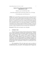
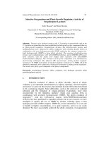
A simple experimental set-up was used for LIE, which consisted of a
continuous wave (CW) argon-ion laser, reflecting mirror, focusing lens and
plastic container, as shown in Figure 1. The laser beam 2.41 eV (λ = 514.5 nm)
was reflected by an aluminium coated highly reflecting mirror (99.5%) and
focused onto a sample of 1.5 mm diameter by using a suitable quartz lens with
focal length of 10 cm and 5 cm in diameter. This lens was mounted on a
micrometer holder for the focusing adjustment. The laser beam power density
required for the LIE process of GaP was varied up to 12 W/cm
2
.
Journal of Physical Science, Vol. 18(2), 49–57, 2007 51
Argon-ion laser (
λ
= 514.5 nm)
Power density = 1.5–12 W/cm
2
Irradiation time = 5–15 min
Spot size = 1.5 mm
Sample: GaP (n-type)
Etching solution: HF 40%
Rinsing with Ethanol
Dry in air
Argon-ion laser
X-Y Translation
Figure 1: The LIE set-up.
Plastic container
HF acid
GaP wafer
Teflon paltes
Focusing lens
Mirror
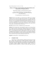
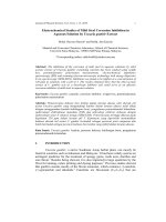
The GaP wafers (n-type) were rinsed with ethanol for 10 min to clean the
surface and then immersed in aqueous 40% wt. HF acid. The immersed wafer
was mounted on two Teflon plates in order to allow the current that could pass
from bottom to top area (irradiation area) through electrolyte, with suitable power
density and irradiation time (IT), as shown in Figure 2. The etching was carried
out at a laser power density of 12 W/cm
2
and 15 min IT. An argon-ion laser beam
of energy (514.5 nm) was used for recording the Raman spectrum.
A special thermodynamic cell was used for the temperature dependence studies.
Temperature Dependence of Raman Spectra 52
Figure 2: Schematic diagram of LIE process.
3. RESULTS AND DISCUSSION
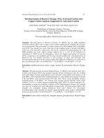
3.1. Raman Spectrum of Porous GaP
The Raman spectrum of porous GaP sample prepared using the LIE
technique is shown in Figure 3. The Raman peak position shifted to a lower
frequency of 398 cm
–1
after etching.
320 340 360 380 400 420 440
LO
Surface Phonon
Bulk GaP
402 cm
-1
Raman Intensity (a.u.)
W
TO
avenumber(cm
-1
)
Wavenumber (cm
–1
)
Figure 3: Raman spectrum of GaP nanostructure prepared by LIE.
Journal of Physical Science, Vol. 18(2), 49–57, 2007 53
The Raman line is broad and asymmetric in comparison to the Raman
line for crystalline GaP, which has a narrow and symmetric shape centered at
402 cm
–1
at room temperature. The weak structure near 349 cm
–1
is a forbidden
transverse optical (TO) phonon, which arises due to structural disorder in the
material. The peak that appears near 378 cm
–1
is attributed to a surface phonon
mode.
The downward shift of the longitudinal optical (LO) phonon frequency
and an increase broadening is apparent. The theoretical fit to the experimental
curve is obtained using a three-dimensional quantum confinement model
incorporating appropriate size distribution.
3.1.1. The crystallite size distribution in porous GaP
The observed broad Raman line shape is a consequence of the crystallite
size distribution around a mean value L
0
as well as the confining geometry. The
size distribution function that we have used is a Guassian:
7
0
2
()
11
() exp
2
2
LL
L
−−
Φ= ⋅⋅
σ⋅σ
⋅π
⎡
⎤
⎢
⎥
⎣
⎦
where, and
0
L
σ
are the mean and standard deviation of the crystallite size
distribution, respectively. The Gaussian functions for the crystallite size
distribution in the phonon confinement model have been used for the total Raman
intensity, which may be written as:
2
1
(,) () (,)
L
IL LILd
L
ω=Φ⋅ω
∫
L
The peak position for the Raman mode is determined by L
0
. L
1
and L
2
are the
minimum and maximum contributing nanocrystallites sizes (1 and 10 nm,
respectively). In this work, these are taken as fitting parameters in Figure 3, as
shown in Table 1. A change in the mean nanocrystallite size, L
0
leads to the shift
in Raman peak position, and variations of L
1
and L
2
values lead to changes in the
Raman line shape broadening without changing the peak position.
Table 1: Fitting parameters of Figure 3.
Excitation
photon
energy (eV)
L
0
(nm)
L
1
(nm)
L
2
(nm)
σ
(nm)
FWHM
(cm
–1
)
Raman peak
position (cm
–1
)
2.41 3 1 10 5 6.5 398
Temperature Dependence of Raman Spectra 54
The average size estimated from the fitting procedure is 3 nm. The
broadening of Raman line is caused by the size distribution, which is dependent
on etching parameters. We have observed another two weak Raman lines besides
the intense LO phonon line at 398 cm
–
1
.
The weak structure near 349 cm
–1
is a forbidden TO phonon, which
arises due to structural disorder in the material. The peak at 378 cm
–1
is attributed
to a surface phonon mode. The surface phonon frequency critically depends on
the nanocrystalline size, shape and dielectric constant of the surrounding
medium. We have calculated the surface phonon frequency (
s
ω
) by considering
a shape using:
8
(
)
(
)
2
2
0
ω
11
= ε + ε 1/ε +ε 1
ω
mm
s
LL
T
∞
⎡⎤⎡
⎣⎦⎣
−−
⎤
⎦
where
T
ω
is the frequency of the TO phonon,
0
ε
= 11.01 and
∞
ε
= 9.09 are the
static and high frequency dielectric constant, respectively
m
ε
= 1.00 and L is the
depolarizing factor.
The calculated value of surface phonon frequency in air for cylindrical
shape is in good agreement with the observed value, as shown in Table 2.
Table 2: Surface phonon frequency in air.
Surface phonon
Peak (cm
–1
)
TO phonon
Peak (cm
–1
)
Dielectric constant
0
ε
∞
ε
m
ε
Depolarizing
Factor L
378 349 11.01 9.09 1.00 0.3
3.2 Temperature Dependence of Raman Spectra
3.2.1 Crystalline and nanocrystalline GaP
Theoretical calculations were performed for the temperature dependence
of the line-center and line-width of the first-order LO-phonon mode in GaP
crystal. The variations in the line-center and line-width with temperature are
shown in Figures 4 and 5, respectively. A decrease in the line-width and a shift in
the line-center toward higher frequencies are indicated as the temperature is
lowered.
9
0
ω
and the constants A, C for GaP at 0 K are listed in Table 3.
Journal of Physical Science, Vol. 18(2), 49–57, 2007 55
The constants A and C at 0 K used in the calculation of phonon shift
0
ω
and
broadening for GaP nanocrystals are listed in Table 4.
0 50 100 150 200 250 300 350 400 450 500
399.0
399.5
400.0
400.5
401.0
401.5
402.0
402.5
403.0
403.5
Raman Shift (cm
-1
)
Temperature (K)
GaP LO-Phonon
Raman Shift (cm
–1
)
Figure 4: Temperature dependence of line-center of LO phonon.
0 50 100 150 200 250 300 350 400 450 500
3
4
5
6
7
8
Raman Linewidth (cm
-1
)
Temperature (K)
L
O Phonon Linewidth
LO
p
honon Line-width
Raman Line-width (cm
–1
)
Figure 5: Temperature dependence of line-width of LO phonon.
Temperature Dependence of Raman Spectra 56
Table 3: Parameters used for temperature dependence on crystalline GaP.
C (cm
–1
) A (cm
–1
)
Γ (cm
–1
)
0
ω
(cm
–1
) at 0 K
– 2.457 1.266 3.3 403
Table 4: Parameters used for temperature dependence on GaP nanocrystalline.
C (cm
–1
) A (cm
–1
)
Γ (cm
–1
)
0
ω
(cm
–1
) at 0 K
– 3.668 2.558 3.3 395
4. CONCLUSION
The charge transfer occurs at the semiconductor-electrolyte interface
when a semiconductor is immersed in aqueous solution, which contains the
electron acceptor species. The employment of modulated photocurrent produces
the photo-generated holes that are directly transferred to the electrolyte solution,
which surrounds the pores material.
High surface quality along with a slight blue shifted emission, due to the
quantum-size effect, indicates that the anodization method is promising for the
fabrication of high-quality quantum wire structures. The softening and
broadening of the optical phonon line in the Raman spectrum also explains the
reduction of the coherence length of phonons. The Raman studies of nanocrystals
provide information on the behavior of the fundamental optical and vibrational
properties. Since Raman scattering is very sensitive to the lattice microstructure,
a phonon confinement model is employed to explain the Raman shift of phonon
modes of a nanocrystal and describes the size confinement effect on lattice
vibration wave functions.
The Raman scattering spectrum of porous GaP has a number of
characteristic features. Both LO and TO phonons are always simultaneously
present in the porous GaP spectra. The surface phonon frequency critically
depends on the nanocrystalline size, shape and dielectric constant of the
surrounding medium.
The line-center as well as line-width varies with temperature in bulk
materials, and this temperature dependence has been attributed to the anharmonic
terms in the vibrational potential energy. It is observed that the line-width
decreased and the line-center shifted toward higher frequencies at low
Journal of Physical Science, Vol. 18(2), 49–57, 2007 57
temperature. It indicates that the phonon lifetime decrease with increasing
temperature.
The exact determination of the positions and line-width of these
microscopic gap modes open a new field of application in studying surface
bonding, anharmonicity effects and coupling to other excitations.
5. REFERENCES
1. Kanemitsu, Y. (1995). Light emission from porous silicon and related
materials. Phys. Rep., 263(1), 1–91.
2. Meijerink, M., Bol, A.A. & Kelly, J.J. (1996). The origin of blue and
ultraviolet emission from porous GaP. Appl. Phys. Lett., 69, 2801–2803.
3. Zoteev, A.V., Kashkarov, P.K., Obraztov, A.N. & Timoshenko, V.Y
(1996). Electrochemcial formation and optical properties of porous
gallium phosphide. Semiconductors, 30, 775–777.
4. Takagahara, T. & Takeda, K. (1992). Theory of the quantum
confinement effect on excitons in quantum dots of indirect-gap materials.
Phys. Rev. B, 46, 15578–15581.
5. Richter H., Wang, Z.P. & Ley, L. (1981). The onee phonon Raman
scattering in microcrystalline silicon. Solid-State Commun., 39, 625–629.
6. Campbell, I.H. & Fauchet, P.M. (1986). The effects of microcrystal size
and shape on the one phonon Raman spectra of crystalline
semiconductors. Solid-State Commun., 58, 739–741.
7. Mavi, H.S., Rasheed, B.G., Shukla, A.K., Abbi, S.C. & Jain, K.P. (2001).
Spectroscopic investigations of porous silicon prepared by laser-induced
etching of silicon. J. Phys. D: Appl. Phys., 34, 292–298.
8. Erne’, B.H., Vanmaekelbergh, D. & Kelly, J.J. (1996). Morphology and
strongly enhanced photoresponse of GaP electrodes made porous by
anodic etching. J. Electrochem. Soc., 143, 305–314.
9. Klemens, P.G. (1966). Anharmonic decay of optical phonons. Phys. Rev.,
148, 845–848.