WILEY ANTENNAS FOR PORTABLE DEVICES phần 4 pot
Bạn đang xem bản rút gọn của tài liệu. Xem và tải ngay bản đầy đủ của tài liệu tại đây (1.06 MB, 30 trang )
74 RFID Tag Antennas
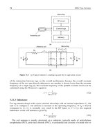
RF circuit
Antenna coil
Control logic
Memory
Microchip
(a)
C
r
U
i
C
p
R
A
L
R
L
Antenna coil
Microchip
U
o
C = C
p
+ C
r
(b)
Figure 3.6 (a) Typical inductive coupling tag and (b) its equivalent circuit.
of the interaction between tags on the overall performance because the overall resonant
frequency of the two tags directly adjacent to one another is always lower than the resonant
frequency of a single tag [2]. The resonant frequency of the parallel resonant circuit can be
calculated using the Thomson’s equation:
f =
1
2
√
L ·C
(3.2)
3.3.1.3 Inductance
For tag antenna design with a prior selected microchip with an internal capacitance C
r
, the
task is to configure a coil antenna to resonate at the operating frequency. If C
p
is known
(compared to C
r
, C
p
is normally very small in the HF band, so C ≈ C
r
, the required
inductance of the coil antenna is given by
L =
1
2f
2
C
(3.3)
The coil antenna is usually structured on a substrate, typically made of polyethylene
terephthalate (PET), polyvinyl chloride (PVC), or polyamide and consists of wound wire or
3.3 Design Considerations 75
etched copper/aluminum strips. Conductive polymeric thick film pastes can also be used for
the coil antenna by screen printing or dispensing for cost reduction. Etched or screen printed
coil antennas are suitable for HF systems because low inductance is required. There are
many types of inductors that can be used to realize the required inductance, and the spiral
inductor is widely used in HF RFID systems.
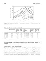
A typical spiral inductor is illustrated in Figure 3.7. The conductive strip is wound either
clockwise or counterclockwise. This configuration ensures that the current in adjacent tracks
is in phase. The resulting mutual inductance yields a significant increase in the spiral
inductor’s self-inductance. Connecting the microchip to the open ends of the spiral antenna
forms a tag. The microchip can be directly connected to the inner and outer ends of the spiral
inductor. It is more convenient to use an underpass to connect the end of the outer turn to
the centre for microchip assembly if more windings are required for a larger inductance.
The inductance of the spiral inductor is determined by its area (L× D and the number of
windings [15]. The width of the tracks and the spacing between them are usually uniform,
although they can be non-uniform. The spiral inductor can be any closed loop such as
a square, rectangle, triangle, circle, semi-circle, or ellipse. The square spiral inductor has
been widely used in practical applications because of its simple layout.
No analytical formula can be used to calculate the inductance of such spiral inductors.
The calculation must instead be done by numerical methods. Many commercial software
tools such as ADS, IE3D, and Microwave Studio can be used for this purpose. Figure 3.8
shows the calculated inductance of the spiral inductor shown in Figure 3.7(b) with length
L =50 mm, width D =40 mm, strip width W =1 mm, strip spacing S =0.5 mm, number of
windings N =6, polyester substrate,
r
=4, and thickness h = 50 m. The calculation was
done using IE3D software, based on the method of moments [16]. The inductance is about
2.3 H from 10 MHz to 17 MHz.
3.3.1.4 Parallel Capacitance
If the coil antenna is predetermined, the required capacitance for the parallel capacitor, C,
for a specific operating frequency is given by
C =
1
2f
2
L
(3.4)
For tags operating in frequency range below 135 kHz, a chip capacitor (C
p
≈ 20–220 pF)
is generally required to achieve resonance at the desired frequency. At high frequencies
(13.56 MHz, 27.125 MHz), the required capacitance is usually so low that it can be provided
by the internal capacitance of the microchip and the parasitic capacitance of the coil. In
general, the internal capacitance of the microchip is fixed, thus the inductance of the coil
antenna has to be modified for circuit resonance by varying its geometry.
3.3.1.5 Q Factor
To characterize the coil antenna, the quality factor Q is commonly used. The Q factor is
a measure of the ability of a resonant circuit to retain its energy. A high Q means that a
circuit leaks very little energy, while a low Q means that the circuit dissipates a lot of energy.
76 RFID Tag Antennas
Connection points
for microchip
D
L
(a)
Connection
points for
microchip
D
L
(b)
Figure 3.7 Spiral antenna: (a) same layer connection; (b) using two metal layers with an underpass.
In Figure 3.6, the entire tag circuit can be considered as a parallel RLC circuit, where R
represents the entire ohmic losses of the tag, including the ohmic loss of the coil antenna
and the series resistance of the microchip. In this case, Q can be defined as
Q =
2fL
R
(3.5)
The induced voltage of the coil antenna is proportional to the Q factor. Usually, the Q
factor is maximized for a long reading distance, but it has to be noted that a high Q factor
limits the bandwidth of transmitted data. Therefore, the typical Q value for most tag coil
antennas is about 30–80.
3.3 Design Considerations 77
Frequency, MHz
10 11 12 13 14 15 16 17
Inductance, μH
1
2
3
4
Figure 3.8 Simulated inductance of spiral coil antenna by IE3D.
3.3.1.6 Case Study
In this section, an example is presented to demonstrate the method for designing a coil
antenna with a prior selected microchip. Important issues such as the essential procedures of
getting necessary information from a microchip datasheet, determining required inductance,
configuring and simulating the coil antenna, and calculating the Q factor will be addressed.
The EM4006 microchip [17] is a CMOS integrated circuit used in electronic read-only
transponders and operating at 13.56 MHz. Generally, the characteristics of the microchip
can be found in the datasheet provided by the manufacturer. The most important pieces
of information for coil antenna design are the internal capacitance of the chip and the
pad position configuration of the microchip. The electrical parameters and pad position of
EM4006 are shown in Table 3.3 and Figure 3.9, respectively. Once we have the information,
we can carry out the coil antenna design.
Calculating Required Inductance of Coil Antenna
The internal capacitance, C
RES
, shown in Table 3.3, is required in coil antenna design. It
is found that the typical value of C
RES
is 94.5 pF at 13.56 MHz. Using (3.3), the required
inductance of the coil antenna is:
L =
1
2 ×314 ×1356 ×10
6
2
×945 ×10
−12
= 146 H (3.6)
Coil Antenna Configuration and Simulation
Having calculated the required inductance of the coil antenna, the next step is to configure
a coil antenna according to the specific design requirements such as size constraint and the
properties of the substrate used. The shape of the coil can be square, rectangle, triangle,
ellipse, or any other closed structures. Figure 3.10 shows the coil antenna layout in IE3D with
the parameters: L = 47 mm, D =47 mm, strip width W = 1 mm, strip spacing S = 0.5 mm.
The substrate is polyester, 50 m thick (
r
= 4.0, tan = 0.002). With the input impedance
78 RFID Tag Antennas
Table 3.3 Electrical characteristics of EM2006.
Parameter Symbol Test Conditions Min Typ. Max. Unit
Supply voltage V
DD
1.9 V
Supply current I
DD
60 150 A
Rectifier V
REC
I
C1C2
=1 mA, modulator switch on 1.8 V
Voltage drop V
REC
= (V
C1
−V
C2
−V
DD
−V
SS
Modulator ON V
ON1
I
VDD VSS
= 1 mA 1.9 2.3 2.8 V
DC voltage V
ON2
I
VDD VSS
= 10 mA 2.4 2.8 3.3 V
drop
Power on reset V
R
1.2 1.4 1.7 V
V
R
−V
MIN
0.1 0.25 0.5 V
Coil 1 − Coil 2 C
RES
V
coil
= 100m V RMS f =10 kHz 92.6 94.5 96.4 pF
capacitance
Series resistance R
S
3
of CRES
Power supply C
sup
140 pF
capacitor
V
DD
= 2V V
SS
= 0 V f
C1
= 1356 MHz sine wave, V
C1
= 10Vpp centered at V
DD
− V
SS
/2
T
a
= 25˚C, unless otherwise specified.
Z
A
= R
A
+X
A
= 058 +j1240 obtained from IE3D, the inductance of the coil antenna is
given by
L =
X
A
2f
=
1240
2 ×314 ×1356 ×10
6
= 146 H (3.7)
The Q factor of the tag is given by
Q =
X
A
R
A
+R
S
=
1240
058 +3
= 346 (3.8)
Antenna Pad Configuration
Much attention should be devoted to the antenna pad position configuration when the coil
layout is made. The coil tracks at the input of the antenna (antenna pad) must be adequately
configured to fit the pad position of the microchip for tag assembly. A proper antenna
pad configuration enables the microchip to be easily affixed to the antenna, which reduces
rejection rate and the cost of the tag.
Referring to Figure 3.9, the microchip has two pads C
1
, C
2
which are fixed on the ends
of the coil antenna. The distance between C
1
and C
2
is 0.74 mm. The antenna pad should
be configured so that the microchip can be placed and aligned on it properly. The details of
the antenna pad are shown in Figure 3.11. The width of the strips is tapered from 1.0 mm to
0.5 mm; the spacing changes from 1.0 mm to 0.2 mm. This arrangement ensures the proper
affixing of the microchip to the coil antenna as long as the outline of the microchip is kept
within the area of the antenna pads.
3.3 Design Considerations 79
(a)
(b)
VSS
TESTn
C1 C2
14
325
513
772
EM4006
740
1144
1124
316
1800
152
1041
All dimensions in μm
Y
X
C1, C2 pad size : 95 × 95
Other pads size : 76 × 76
TOUT
VDD
EM4006
Figure 3.9 Microchip pad information: (a) pad assignment; (b) pad position.
80 RFID Tag Antennas
Antenna
Pad
1
D
1
L
Figure 3.10 Tag coil antenna configuration.
1.0
1.0
0.5
0.2
2
C
1
C
2
ASIC
Unit: mm
0.74
1.2
Figure 3.11 Details of the antenna pad configuration.
3.3.2 Far-field RFID Tag Antennas
For far-field RFID systems, the tag antenna design plays a vital role in system efficiency and
reliability since the operation of passive RFID tags is based on the EM field they receive
from the readers. Figure 3.3 illustrates the operating principles of a passive far-field RFID
system. The reader sends out a continuous wave RF signal containing alternating current
power and clock signal to the tag at the carrier frequency at which the reader operates. The
RF voltage induced on the antenna terminals is converted to direct current which powers up
3.3 Design Considerations 81
the microchip. A voltage of about 1.2 V is necessary to energize the microchip for reading
purposes. For writing, the microchip usually needs to draw about 2.2 V from the reader’s signal.
Then the microchip sends back the information by varying complex RF input impedance. The
impedance typically toggles between two different states (conjugate matched and some other
impedance) to modulate the backscattering signal. When receiving this modulated signal, the
reader decodes the pattern and obtains the tag information.
3.3.2.1 Radio Link
In an RFID system, the reading distance is constrained by the maximum distance at which
the tag can receive just enough power to turn on and scatter back, and the maximum distance
at which the reader can detect this backscattered signal. The reading distance of an RFID
system is the smaller of these two distances. Typically the reader sensitivity is high enough,
therefore the reading distance is determined by the former distance. The reading distance is
also sensitive to the tag orientation, the properties of the objects to which the tag is attached,
and the propagation environment.
Power Link (Reader to Tags)
Consider the RFID system shown in Figure 3.4, where the output power of the reader is
P
reader-tx
the gain of the reader antenna is G
reader-ant
the distance between the reader antenna
and the tag is R, and the gain of the tag antenna is G
tag-ant
. According to the Friis free-space
transmission formula, the power received by the tag antenna is [18]:
P
tag-ant
=
4R
2
P
reader-ant
G
reader-ant
G
tag-ant
(3.9)
where is the wavelength in free space at the operating frequency and is the polarization
matching coefficient between the reader antenna and tag antenna. If the two antennas are
perfectly matched in polarization, will be 1 or 0 dB. For most of far-field RFID systems,
the reader antenna is circularly polarized while the tag antenna is linearly polarized, hence
will be 0.5 or −3 dB.
Part of the power received by the tag antenna is delivered to the terminating microchip,
and it can be expressed as:
P
tag-chip
= P
tag-ant
(3.10)
where is the power transmission coefficient determined by the impedance matching between
the tag antenna and the microchip.
The maximum reading distance for a radio power link is obtained when P
tag-chip
is equal
to the threshold power of the microchip, P
tag-threshold
, which is the minimum threshold power
to power up the microchip on the RFID tag:
R
power−link
=
4
P
reader−tx
G
reader-ant
G
tag-ant
P
tag−threshold
(3.11)
For convenience, (3.11) can be modified as:
R
power−link
= 10
m (3.12)
82 RFID Tag Antennas
where
=276 −20 logfMHz+P
reader-tx
dBm+G
reader-ant
dBic
+
G
tag-ant
dBi +dB +dB −P
tag-threshold
dBm
20
Backscatter Communication Link
The backscatter communication link from the tags to the reader is largely dependent on the
backscatter field strength of the tag. Based on a monostatic (backscattering) radar equation
[19], the amount of modulated power received by the reader is given by:
P
reader-rx
=
2
4
3
R
4
P
reader−tx
G
2
reader-ant
(3.13)
where is the radar cross-section (RCS) of the RFID tag.
When the received power is equal to the reader’s sensitivity, P
reader-threshold
, the maximum
distance for backscatter communication link can be obtained:
R
backscatter
=
4
2
4
3
P
reader-tx
G
2
reader-ant
P
reader-threshold
(3.14)
Again (3.14) can be expressed in a modified form:
R
backscatter
= 10
m (3.15)
where
=166 −20 log
f
MHz
+P
reader-tx
dBm
+2G
reader-ant
dBic
+
dB +dBsm −P
reader-threshold
dBm
40
From (3.11) and (3.14) it is observed that the reading distance is determined by the output
power of the reader, P
reader-tx
and the gain of the reader antenna, G
reader-ant
, the gain of the tag
antenna, G
tag-ant
, the polarization matching coefficient, , the power transmission coefficient
of the tag, , the RCS of the tag, , the threshold power of the microchip, P
tag−threshold
, and
receiver sensitivity of the reader, P
reader−threshold
. The last two parameters are predetermined
for a prior selected reader and microchip. The remaining parameters can be optimized to
achieve a longer reading distance. The above-mentioned parameters will be addressed in the
following sections.
3.3.2.2 EIRP and ERP
As mentioned in Section 3.3.2.1, the maximum reading distance is proportional to the output
power of the reader and the gain of the reader antenna. Higher output power and gain of
the reader antenna can offer a longer reading distance. However, the output power is always
limited by national licensing regulations.
3.3 Design Considerations 83
EIRP is the measure of the radiated power which an isotropic emitter (i.e. G =1or0dB)
will need to supply in order to generate a defined radiation power at the reception location
as at the device under test [2]:
P
EIRP
= P
reader-tx
G
reader-ant
(3.16)
In addition to the EIRP, ERP is frequently used in radio regulations and in the literature.
The ERP relates to a dipole antenna rather than an isotropic emitter. It expresses the radiated
power which dipole antenna (i.e. G = 164 or 2.15 dB) will need to supply in order to
generate a defined radiation power at the reception location as at the device under test.
It is easy to convert between the two parameters:
P
EIRP
= 164P
ERP
(3.17)
Table 3.2 summarizes regulated EIRP or ERP in the UHF band for different countries/
regions.
3.3.2.3 Tag Antenna Gain
The tag antenna gain, G
tag-ant
, is the other important parameter for the reading distance. The
range is largest in the direction of maximum gain which is fundamentally limited by the size,
radiation patterns of the antenna, and the frequency of operation. For a small dipole-like
omnidirectional antenna, the gain is about 0–2 dBi. For some directional antennas such as
the patch antenna, the gain can be up to 6 dBi or more.
3.3.2.4 Polarization Matching Coefficient
The polarization of the tag antenna must be matched to that of the reader antenna in order
to maximize the reading distance, which can be characterized by the polarization matching
coefficient, . For far-field RFID systems, the reader antenna is always circularly polarized
because the orientation of the tag is random. Using a linearly polarized tag antenna will result
in a polarization mismatch loss, i.e. = 0.5 or −3 dB. A circularly polarized tag antenna is
preferable for some specific applications because the signal can be increased by 3 dB.
3.3.2.5 Power Transmission Coefficient
Referring to Figure 3.12, consider a tag antenna with a maximum effective aperture A
e-max
(in square meters), situated in the field of the reader antenna with the power density S (watts
per square meter). It takes in power from the wave and delivers it to the termination, namely
the microchip with load impedance Z
T
. Part of the power received by the tag antenna is
delivered to the termination while the rest of the power is reflected and re-radiated by the
antenna. The amount of the power delivered to the microchip can be quantified by using the
power transmission coefficient, . Let the power antenna received from the incident wave
be P
tag-ant
, and the power delivered to the chip P
tag-chip
. Then
P
tag-ant
= SA
e-max
(3.18)
84 RFID Tag Antennas
P
tag-chip
= P
tag-ant
(3.19)
The power transmission coefficient, , is determined by the impedance matching between the
tag antenna and the microchip. Proper impedance matching between antenna and microchip
is of paramount importance in RFID since IC design and manufacturing are a big and costly
venture. RFID tag antennas are normally designed for a specific microchip available on the
market. Adding an external matching network with lumped elements is usually prohibitive
in RFID tags due to cost and fabrication issues. To alleviate this situation, the tag antenna
can be directly matched to the microchip which has complex impedance that varies with the
frequency and the input power supplied to the microchip.
In the equivalent circuit shown in Figure 3.12(b), Z
T
= R
T
+jX
T
is the complex chip
impedance and Z
A
= R
A
+jX
A
is the complex antenna impedance. The chip impedance
includes the effects of chip package parasitics. Both Z
A
and Z
T
are frequency-dependent. In
addition, the impedance Z
T
may vary with the power delivered to the chip.
To describe the transmission of the power waves, we introduce a power wave reflection
coefficient [20]:
=
Z
T
−Z
∗
A
Z
T
+Z
A
0 ≤≤1 (3.20)
The power delivered to the chip is
P
tag-chip
=
1 −
2
P
tag-ant
(3.21)
The power transmission coefficient can be expressed as:
=
P
tag-chip
P
tag-ant
= 1 −
2
=
4R
A
R
T
R
A
+R
T
2
+
X
A
+X
T
2
0 ≤ ≤ 1 (3.22)
When the antenna is conjugately matched to the chip, i.e. R
T
= R
A
and X
T
=−X
A
, then
=0, = 1.0, and the corresponding maximum transferred power is
P
tag-chip−max
= P
tag-ant
= SA
e−max
(3.23)
When the antenna is shorted, the chip resistance R
T
=0 and the chip reactance X
T
=−X
A
,
will be unity and zero. Thus, there is no power delivered to the chip.
It is convenient to relate the power transmission coefficient, , to another widely used
parameter, return loss (RL), for describing the impedance matching characteristics. The return
loss is defined as:
RL = 10 log
10
(3.24)
It is convenient to obtain the return loss from simulation or/and measurement. With the
return loss, the corresponding reflection coefficient and the power transmission coefficient
can be easily calculated. Table 3.4 shows the corresponding reflection coefficient and power
transmission coefficient for different return losses. Figure 3.13 illustrates the relationship
between the power transmission coefficient and the return loss.
3.3 Design Considerations 85
S
Micro
chip
Tag antenna
P
tag-ant
P
tag-chip
P
tag-ref
(a)
V
Z
A
= R
A
+ j X
A
Tag antenna
Z
T
= R
T
+ j
X
T
Microchip
P
tag-ant
P
tag-chip
P
tag-ref
(b)
Figure 3.12 Power transfer in the RFID tag and its equivalent circuit: (a) power transfer in RFID
tag configuration; (b) equivalent circuit.
3.3.2.6 Antenna RCS
As seen from (3.14), the maximum distance for the backscatter communication link is
proportional to the RCS of the RFID tag antenna. In this section, the method of quantifying
the RCS of a RFID tag antenna will be introduced.
Radar cross-section definition
The RCS is a measure of the amount of power scattered in a given direction when an object
is illuminated by an incident wave. The IEEE defines RCS as 4 times the ratio of the
power per unit solid angle scattered in a specified direction to the power per unit area in
Table 3.4 Reflection coefficient and transmission coefficient as function of return loss.
Return Reflection Transmission Transmission Return Reflection Transmission Transmission
Loss(dB) coefficient
coefficient() coefficient(, dB) loss (dB) coefficient
coefficient () coefficient (, dB)
0.0 1.0000 0.0000 − −10.0 0.3162 0.9000 −0.4576
−0.5 0.9441 0.1087 −9.6357 −11.0 0.2818 0.9206 −0.3594
−1.0 0.8913 0.2057 −6.8683 −12.0 0.2512 0.9369 −0.2830
−1.5 0.8414 0.2921 −5.3454 −13.0 0.2239 0.9499 −0.2233
−2.0 0.7943 0.3690 −4.3292 −14.0 0.1995 0.9602 −0.1764
−2.5 0.7499 0.4377 −3.5886 −15.0 0.1778 0.9684 −0.1396
−3.0 0.7079 0.4988 −3.0206 −16.0 0.1585 0.9749 −0.1105
−3.5 0.6683 0.5533 −2.5703 −17.0 0.1413 0.9800 −0.0875
−4.0 0.6310 0.6019 −2.2048 −18.0 0.1259 0.9842 −0.0694
−4.5 0.5957 0.6452 −1.9031 −19.0 0.1122 0.9874 −0.0550
−5.0 0.5623 0.6838 −1.6509 −20.0 0.1000 0.9900 −0.0436
−5.5 0.5309 0.7182 −1.4378 −22.0 0.0794 0.9937 −0.0275
−6.0 0.5012 0.7488 −1.2563 −24.0 0.0631 0.9960 −0.0173
−6.5 0.4732 0.7761 −1.1007 −26.0 0.0501 0.9975 −0.0109
−7.0 0.4467 0.8005 −0.9665 −28.0 0.0398 0.9984 −0.0068
−7.5 0.4217 0.8222 −0.8504 −30.0 0.0316 0.9990 −0.0043
−8.0 0.3981 0.8415 −0.7494 −35.0 0.0178 0.9997 −0.0013
−8.5 0.3758 0.8587 −0.6614 −40.0 0.0100 0.9999 −0.0004
−9.0 0.3548 0.8741 −0.5844 −45.0 0.0056 1.0000 −0.0000
−9.5 0.3350 0.8878 −0.5169 −50.0 0.0033 1.0000 −0.0000
3.3 Design Considerations 87
Return Loss, dB
–20 –15 –10 –5 0
Transmission coefficient, τ, dB
–20
–15
–10
–5
0
Figure 3.13 Transmission coefficient vs return loss.
a plane wave incident on the scatter from a specified direction. More precisely, it is the
limit of that ratio as the distance from the scatter to the point where the scattered power is
measured approaches infinity [19]:
= lim
R→
4R
2
E
scat
2
E
inc
2
(3.25)
Where E
scat
is the scattered electric field from the object and E
inc
is the incident field on
the object.
The RCS can also be given in another form:
= 4R
2
S
scat
S
inc
(3.26)
where S
scat
indicates the scattered power density, S
inc
is the incident power density at the
scattering object, andR denotes the distance from the object.
The RCS is given in units of square meters. However, this does not necessarily relate to
the physical size of an object although it is generally true that larger physical objects have
larger radar cross-sections. Typical values of RCS span from 10
−5
m
2
for insects to 10
+6
m
2
for a large ship. Due to the large dynamic range of the RCS, a logarithmic power scale is
most often used with the reference value of
ref
= 1m
2
:
dBsm
=
dBm
2
= 10 log
10
m
2
ref
= 10 log
10
m
2
1
(3.27)
There are three types of scattering from an object: monostatic or backscattering, where
the incident and pertinent scattering directions are coincident but opposite in sense; forward
scattering, where the incident and pertinent scattering directions are the same; and bistatic
88 RFID Tag Antennas
scattering, where the two directions are different. In far-field RFID systems, backscattering
is used in the transmission of data from a tag to a reader.
The RCS of an object is dependent on a range of parameters, such as size, shape, material,
surface structure, polarization, and the operating wavelength. The dependence of the RCS
on the operating wavelength generally divides objects into three categories:
•
Rayleigh range. The wavelength is much greater than the object dimensions, so there is
little variation in phase over the length of the body. For objects smaller than around half
the wavelength, the RCS exhibits a
−4
dependency and therefore the reflective properties
of objects smaller than 0.1 can be disregarded in practice.
•
Resonance range. The wavelength is comparable with the object dimensions – typically
the object dimensions are taken to be between and 10. In this range, the electromagnetic
energy shows a tendency to stay attached to the object’s surface to create surface waves
including traveling waves, creeping waves, and edge traveling waves. Objects with sharp
resonance, such as sharp edges, slits and points, may at certain wavelengths exhibit
resonance set-up of RCS. Under certain circumstances, this is particularly true for antennas
that are being irradiated at their resonant wavelength.
•
Optical range. The wavelength is much smaller than the dimensions of object. In this
case, only the geometry and position (angle of incidence of the electromagnetic wave) of
the object influence the RCS.
Antenna Scattering
Backscattering RFID systems employ antennas with different configurations as scatters. As
antennas are always designed to transmit and receive EM waves, they are generally regarded
as having two modes of scattering [19, 21]. The first is structural mode, the scattering that
occurs because the antenna is of a given shape, size, and material and is independent of the
fact that the antenna is specially designed to transmit or receive RF energy. The second is
antenna mode, the scattering that has to do directly with the fact that the antenna is designed
to radiate or receive RF energy and has a specific radiation pattern. The principles of antenna
scattering modes are presented in Figure 3.14.
The antenna RCS, , can conceptually be defined as
=
struct
+
ant
(3.28)
Although the concept of dividing the antenna RCS into two components is simple and
easily grasped, it should be noted that there is no formal definition of these scattering
modes [19].
(a) (b)
Figure 3.14 Antenna scattering: (a) antenna mode; (b) structural mode.
3.3 Design Considerations 89
Antenna-mode RCS Equations
As discussed in Section 3.3.2.5, a tag antenna situated in the field radiated from the reader
antenna collects the power from the incident wave and delivers part of it to the termination,
namely the microchip with load impedance Z
T
. The rest of the power is re-radiated into space
by the tag antenna. The tag and its equivalent circuit are redrawn and shown in Figure 3.15
to illustrate the scattering mechanism of the antenna. The real part of the antenna impedance
is split into two parts: the radiation resistance, R
r
, and the ohmic loss resistance, R
L
.
Referring to Figure 3.15, the voltage source represents an open circuit RF voltage applied
on the terminals of the receiving antenna, and produces a current I through the antenna
impedance Z
A
and the terminating impedance Z
T
. The current I is determined by the quotient
Reader
Reader antenna
Incident wave
ASIC
Tag antenna
Scattered wave
(a)
V
Z
A
=
(R
r
+
R
L
)
+
j
X
A
Z
T
=
R
T
+
jX
T
I
(b)
Figure 3.15 Schematic diagram of far field RFID tag scattering: (a) plane wave receiving and re-
radiating of tag antenna; (b) equivalent circuit of the tag.
90 RFID Tag Antennas
of the induced voltage V and the series connection of the individual impedances [18]:
I =
V
Z
A
+Z
T
=
V
R
r
+R
L
+R
T
+j
X
A
+X
T
(3.29)
where I and V are the RMS or effective values.
The power delivered by the antenna to the microchip is
P
tag-chip
=I
2
R
T
=
V
2
R
T
R
r
+R
L
+R
T
2
+
X
A
+X
T
2
(3.30)
The effective aperture A
e
of the antenna is the quotient of the received power P
tag-chip
and
the incident wave density:
A
=
e
P
tag-chip
S
=
V
2
R
T
S
R
r
+R
L
+R
T
2
+
X
A
+X
T
2
(3.31)
If the terminating impedance is the complex conjugate of the antenna impedance, i.e.
R
T
= R
L
+R
r
, and X
A
=−X
T
, the maximum effective aperture of the antenna is obtained:
A
e−max
=
V
2
4SR
T
(3.32)
As can be seen from Figure 3.15, the current also flows through the antenna impedance
Z
A
. The real part of the impedance, R
A
has two parts: the ohmic loss resistance R
L
, and
the radiation resistance R
r
, R
A
= R
L
+R
r
. Therefore, some of the power will be dissipated
as heat in the antenna as given by:
P
L
=
I
2
R
L
(3.33)
The reminder is ‘dissipated’ in the radiation resistance. In other words, it is re-radiated
into space by the antenna. This re-radiated power can be written as:
P
s
=
I
2
R
r
=
V
2
R
r
R
r
+R
L
+R
T
2
+
X
A
+X
T
2
(3.34)
The scattering aperture of the antenna, A
S
, or the antenna-mode RCS of the antenna can
be defined as the ratio of the re-radiated power to the power density of the incident wave:
ant
= A
S
=
P
s
S
=
V
2
R
r
S
R
r
+R
L
+R
T
2
+
X
A
+X
T
2
(3.35)
If the antenna is operating under a maximum power transfer condition and lossless, that
is R
L
= 0, R
r
= R
T
, and X
A
=−X
T
, in which case
ant
= A
S
=
V
2
4SR
r
(3.36)
3.3 Design Considerations 91
Therefore, in the case of conjugate impedance matching condition,
ant
= A
S
= A
e−max
.
This suggests that only half of the total power drawn from the incident wave is supplied to
the terminating resistor R
T
; the other half is re-radiated into the space by the antenna. When
antenna is resonant short circuited [18], with R
T
=0, and X
T
=−X
A
. The antenna-mode
RCS of the antenna can be expressed as
ant-max
= A
S−max
=
V
2
SR
r
= 4A
e−max
(3.37)
As a result, for the resonant short-circuit condition, the antenna-mode RCS is 4 times as
great as its maximum effective aperture.
For the case when the antenna is open circuited, i.e. Z
T
→; it is easy to get:
ant-min
= A
S-min
= 0
Z
T
→
(3.38)
The antenna-mode RCS can thus take any desired value in the range 0–4A
e-max
at varying
values of the terminating impedance Z
T
(as shown in Figure 3.16). In Particular, the antenna-
mode RCS is ideally 4 times (or 6 dB) larger for the resonant short circuit relative to the
conjugate matched case. This property is utilized for the data transmission from tag to reader
in backscattering RFID systems.
It should be noted that the RCS can only be precisely calculated for simple structures –
spheres, flat surfaces, and the like. Analytical derivation of the RCS of an antenna with
R
T
/R
A
012345678910
Relative A
e,
σ
ant
0
1
2
3
4
A
e
σ
ant
Figure 3.16 Variation of the effective aperture, antenna-mode RCS as a function of the ratio of the
resistance R
T
/R
A
. (When R
T
/R
A
= 1 the antenna is operating under a conjugate matched condition.
The case R
T
/R
A
= 0 represents a resonant short circuit at the terminals of the antenna. It is assumed
that R
L
= 0, and X
A
=−X
T
)
92 RFID Tag Antennas
Frequency, MHz
800 850 900 950 1000
RCS, dBsm
–40
–35
–30
–25
–20
–15
–10
Z
T
= 0– j362.5
Z
T
= 57.16– j362.5
Z
T
= 10000– j362.5
Z
T
= 57.16 + j362.5
at 900 MHz
103 mm
11.4
mm
W=1
mm
43.8 mm
Figure 3.17 RCS of a folded dipole antenna with different terminating impedances, calculated by
IE3D.
an arbitrary structure is difficult. Numerical methods such as the method of moments are
generally used for antenna RCS calculation.
As an example to show the variation of antenna RCS with different terminating
impedances, the RCS of a folded dipole antenna with three terminating conditions is shown
in Figure 3.17. The impedance of the antenna is Z
A
= 5716 +j3625 at 900 MHz. When
the antenna is resonant short-circuited, i.e. Z
T
= 0 −j3625 , the RCS of the antenna is
maximum,
ant-short
=−12.55 dBsm. When the antenna is conjugate matched, i.e. Z
T
=
5316 −j3625 ,
ant-matched
=−18.51dBsm. It is observed that
ant-short
is 6 dB larger than
ant-matched
. For a higher terminating impedance of Z
T
= 1000 −j3625,asR
T
/R
A
is large,
the RCS of the antenna decreases drastically ( = −36.42 dBsm).
3.3.2.7 Case Study
Microchip Information
A chip with a plastic thin shrink small-outline package is used in this example. The electrical
properties and outline of this chip are shown in Table 3.5 and Figure 3.18, respectively. It
is found that the input impedance of the microchip is Z
T
= 115 −j422 and its threshold
operating power is −13 dBm at 915 MHz.
Tag antenna configuration and simulation
Several types of antennas have been reported to be used as passive far-field tag antennas,
including meander line antennas, [22, 23], folded dipole antennas [24, 25], loop antennas
[26, 27], slot antennas [28, 29], inverted-F antennas [30], planar inverted-F antennas [31, 32],
slotted planar inverted-F antennas [33], patch antennas [34] and so on. Each type of antenna
has its inherent characteristics for specific applications. For instance, a folded dipole antenna
is used to demonstrate the design procedure. Its impedance can be adjusted easily by tuning
3.3 Design Considerations 93
Table 3.5 Table 3.5 Electrical characteristics of the microchip.
Symbol Parameter Conditions Min. Typ. Max. Unit
Z
867
Input impedance T = 22˚C, f = 867 MHz
a
12.7−j457
Z
915
T = 22˚C, f = 915 MHz
a
11.5−j422
Z
1450
T = 22˚C, f = 2450 MHz
a
3.7−j60.2
Z
867
Minimum f = 867MHz
b
−14 dBm
Z
915
operating power f = 915 MHz
b
−13 dBm
Z
1450
f = 2450 MHz
b
−8 dBm
a
Measured at typical ‘Minimum operating power’.
b
Values apply for operation with low modulation index (18%) and high return data rate (4 times
forward link).
P1P8
0.25–
0.45
mm
0.65
mm
(a)
2.9–3.1 mm
0.15–
0.28
mm
4.7–5.1mm
0.4–0.7
mm
(b)
Figure 3.18 Package outline of the chip: (a) top view; (b) side view.
the length and width of the dipole. The antenna is structured on an FR4 substrate of 20 mils
thickness, as shown in Figure 3.19.
According to (3.11) and (3.14), in order to determine the reading distance of the tag,
the gain of the tag antenna, G
tag-ant
, the power transmission, , and the RCS of the tag
antenna, should be known. The gain of tag antenna cannot be directly obtained from
simulation or measurement because the calculated or measured gain takes into account
the mismatch loss of the antenna, and that mismatch loss is based on the fact that the
terminating impedance is 50 . However, the RFID tag antenna is always matched to the
impedance of the terminating microchip, and the mismatch loss between the antenna and
94 RFID Tag Antennas
4 mm
14.1 mm
1.5 mm 14.1 mm
32.7 mm
Microchip
88
mm
20
mils
FR4
Figure 3.19 RFID tag with a folded dipole antenna.
Frequency, MHz
Gain, dBi
4
2
0
–2
–4
800 850 900 950 1000
Figure 3.20 Gain of the folded dipole antenna, excluding the mismatch loss, calculated by IE3D.
the terminating microchip is quantified by the transmission coefficient, . The gain of the
tag antenna can be calculated by multiplying the antenna directivity with the radiation
efficiency. The calculated gain of the folded dipole antenna, shown in Figure 3.20, is 0.94 dB
at 915 MHz.
The calculated input impedance of the antenna is shown in Figure 3.21. The real part
varies from 23 to 55 , while the imaginary part is from 250 to 650 over 800–1000 MHz.
The impedance is Z
A
= 340 +j4288 at 915 MHz. The return loss can be calculated
through (3.22) and (3.24) by using Z
A
and Z
T
; it can also be obtained in IE3D by taking
the terminating impedance to be Z
C
= 115 −j422 . The results are shown in Figure 3.22;
the return loss is −584 dB at 915 MHz and the corresponding transmission coefficient is
0.74 or −1.32 dB.
3.3 Design Considerations 95
Frequency, MHz
800 850 900 950 1000
10
20
30
40
50
X
A
, ohms
R
A
, ohms
0
100
200
300
400
500
600
700
R
A
X
A
Figure 3.21 Impedance calculated by IE3D.
Frequency, MHz
800 850 900 950 1000
Return loss, dB
–15
–10
–5
0
Transmission coefficient, τ(dB)
–25
–20
–15
–10
–5
0
RL
τ
Figure 3.22 Calculated return loss and transmission coefficient.
96 RFID Tag Antennas
Frequency, MHz
800 850 900 950 1000
RCS, dBsm
–30
–25
–20
–15
–10
Z
T
=
0 – j422
Z
T
=
11.5 – j422
Figure 3.23 RCS of the folded dipole antenna, calculated by IE3D.
As discussed in Section 3.3.2.6, the RFID tag changes its chip impedance to modulate the
backscattering signal. The microchip can be in either the short-circuited or other impedance
condition. The simulated RCS of the antenna under the two impedance conditions is shown
in Figure 3.23, where the value of is −13.96 dBsm for the short-circuited condition and
−16.11 dBsm for Z
T
= 115 −j422 .
Reading Distance Calculation
Assume that the tag is used with a reader having the following parameters: operating
frequency f = 915 MHz; EIRP = 4W (P
reader-tx
= 30 dBm, G
reader-ant
=6 dBic); sensitivity of
the reader P
reader-threshold
=−65 dBm. The parameters of the tag antenna are: antenna gain
G
tag-ant
= 094 dB; power transmission coefficient of the tag =−132 dB; RCS of the tag
=−1611 dBsm (the smaller value); the polarization matching coefficient is −3dB
because the reader antenna is circularly polarized while the folded dipole is linearly polarized;
the threshold operating power of the chip P
tag-threshold
=−13 dBm. The reading distance can
be calculated by (3.12) and (3.15):
R
power−link
= 500 m (3.39)
R
backscatter
= 1354 m (3.40)
It is evident that the power-up distance, R
power−link
, is smaller than the backscattering
distance, R
backscatter
. The reading distance of the system is thus determined by the smaller
distance. This implies that the main concern in a tag antenna design should be the gain of
the antenna and impedance matching between the antenna and the microchip.
3.4 Effect of Environment on RFID Tag Antennas 97
R
Reader antenna
Stand
Anechoic chamber
Mast
RFID tag
RFID
reader
Figure 3.24 Reading distance measurement in an anechoic chamber.
Reading Distance Measurement
The reading distance can be measured by using a reader including a reader antenna with
a known EIRP. To get more accurate results, the measurement should be conducted in an
anechoic chamber to avoid multipath effects. The maximum distance at which the tag can
communicate with the reader is recorded. The measurement set-up shown in Figure 3.24
uses a SAMSys MP9320 reader with 36 dBm EIRP, and the dimensions of the anechoic
chamber are 10 m × 4m × 4 m. The measured maximum reading distance is 4.85 m, which
agrees with the calculated value (5.0 m) very well. The difference of 0.15 m may be caused
by variation of the parameters of the microchip in terms of the load impedance and the
minimum operating power level.
3.4 Effect of Environment on RFID Tag Antennas
RF tag performance can be affected by many factors, in particular the EM properties of
objects near or in contact with the tag antenna. To date, there have been few published reports
on this topic. Foster and Burberry [11] have performed basic measurements of an antenna
near several objects. Raumonen et al. have studied a similar problem through simulations
[35]. Dobkin and Weigand have also shown experimentally a decrease in the reading distance
of several RF tags near a metal plate and a water-filled container, along with changes in the
RF tag antenna input impedance near a metal sheet [36]. Griffin et al. have presented the
power and backscatter communication radio link budgets that allowed the RF tag designer
to quantify the effects of RF tag material attachment. The term ‘gain penalty’ has been
introduced to describe the decrease in the RF tag antenna gain from its free-space value [37].
Among the objects the tags can attached to, metal and lossy materials such as metal cans
and water are of great interest. The environment effect of these two objects is different for
near-field coil antennas and far-field tag antennas because the EM field behavior differs
dramatically in these two systems.
Water and other liquids have less effect on near-field RFID tags because the longer
wavelengths of near-field systems are less susceptible to absorption. On the other hand,
far-field RFID systems have a shorter wavelength and are more susceptible to absorption
by liquids. In practical applications, near-field tags are more suited for tagging water- or
98 RFID Tag Antennas
liquid-bearing containers. Far-field tags can be made to work, but their effective reading
distance would be drastically reduced.
While all frequencies cannot penetrate through a metal object, absorption by the object
affects near-field and far-field tags differently. The reading distance of near-field tags may
be reduced, whereas that of far-field tags may be increased if there is a certain air gap
between the tag antennas and the metal surface where the object acts as a reflector of the tag
antenna. This situation is unique for each particular application using far-field tags on the
metal surfaces, and the same predictable results cannot be obtained in all cases. In situations
where metallic materials are in part of the application, it is best to make use of the metal
as part of the tag antenna by using the metal as the antenna ground. If this is not possible,
shielding techniques are required.
3.4.1 Near-field Tags
3.4.1.1 Effects of Metal Material on Tag Antenna
Figure 3.25 shows the influence of the metal on the performance of a near-field tag. When the
coil antenna is oriented parallel to a metal surface, the magnetic field generated by the coil
Figure 3.25 Coil antenna close to a metal surface: (a) magnetic field distribution of the coil antenna
with a metal surface; (b) Using ferrite shielding to reduce the metal effect.