Computer organization and design Design 2nd phần 5 pptx
Bạn đang xem bản rút gọn của tài liệu. Xem và tải ngay bản đầy đủ của tài liệu tại đây (333.42 KB, 99 trang )
358 Chapter 4 Advanced Pipelining and Instruction-Level Parallelism
years. Nicolau and Fisher [1984] published a paper based on their work with
trace scheduling and asserted the presence of large amounts of potential ILP in
scientific programs.
Since then there have been many studies of the available ILP. Such studies
have been criticized since they presume some level of both hardware support and
compiler technology. Nonetheless, the studies are useful to set expectations as
well as to understand the sources of the limitations. Wall has participated in sev-
eral such strategies, including Jouppi and Wall [1989], Wall [1991], and Wall
[1993]. While the early studies were criticized as being conservative (e.g., they
didn’t include speculation), the latest study is by far the most ambitious study of
ILP to date and the basis for the data in section 4.8. Sohi and Vajapeyam [1989]
give measurements of available parallelism for wide-instruction-word processors.
Smith, Johnson, and Horowitz [1989] also used a speculative superscalar proces-
sor to study ILP limits. At the time of their study, they anticipated that the proces-
sor they specified was an upper bound on reasonable designs. Recent and
upcoming processors, however, are likely to be at least as ambitious as their pro-
cessor. Most recently, Lam and Wilson [1992] have looked at the limitations im-
posed by speculation and shown that additional gains are possible by allowing
processors to speculate in multiple directions, which requires more than one PC.
Such ideas represent one possible alternative for future processor architectures,
since they represent a hybrid organization between a conventional uniprocessor
and a conventional multiprocessor.
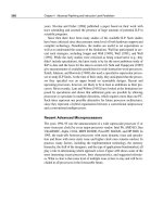
Recent Advanced Microprocessors
The years 1994–95 saw the announcement of a wide superscalar processor (3 or
more issues per clock) by every major processor vendor: Intel P6, AMD K5, Sun
UltraSPARC, Alpha 21164, MIPS R10000, PowerPC 604/620, and HP 8000. In
1995, the trade-offs between processors with more dynamic issue and specula-
tion and those with more static issue and higher clock rates remains unclear. In
practice, many factors, including the implementation technology, the memory
hierarchy, the skill of the designers, and the type of applications benchmarked, all
play a role in determining which approach is best. Figure 4.60 shows some of the
most interesting recent processors, their characteristics, and suggested referenc-
es. What is clear is that some level of multiple issue is here to stay and will be in-
cluded in all processors in the foreseeable future.
4.11 Historical Perspective and References 359
Issue capabilities
SPEC
(measure
or
estimate)Processor
Year
shipped in
systems
Initial
clock rate
(MHz)
Issue
structure
Schedul-
ing
Maxi-
mum
Load-
store
Integer
ALU FP Branch
IBM
Power-1
1991 66 Dynamic Static 4 1 1 1 1 60 int
80 FP
HP 7100 1992 100 Static Static 2 1 1 1 1 80 int
150 FP
DEC Al-
pha 21064
1992 150 Dynamic Static 2 1 1 1 1 100 int
150 FP
Super-
SPARC
1993 50 Dynamic Static 3 1 1 1 1 75 int
85 FP
IBM
Power-2
1994 67 Dynamic Static 6 2 2 2 2 95 int
270 FP
MIPS TFP 1994 75 Dynamic Static 4 2 2 2 1 100 int
310 FP
Intel
Pentium
1994 66 Dynamic Static 2 2 2 1 1 65 int
65 FP
DEC
Alpha
21164
1995 300 Static Static 4 2 2 2 1 330 int
500 FP
Sun
Ultra–
SPARC
1995 167 Dynamic Static 4 1 1 1 1 275 int
305 FP
Intel P6 1995 150 Dynamic Dynamic 3 1 2 1 1 > 200 int
AMD K5 1995 100 Dynamic Dynamic 4 2 2 1 1 130
HaL R1 1995 154 Dynamic Dynamic 4 1 2 1 1 255 int
330 FP
PowerPC
620
1995 133 Dynamic Dynamic 4 1 2 1 1 225 int
300 FP
MIPS
R10000
1996 200 Dynamic Dynamic 4 1 2 2 1 300 int
600 FP
HP 8000 1996 200 Dynamic Static 4 2 2 2 1 > 360 int
> 550 FP
FIGURE 4.60 Recent high-performance processors and their characteristics and suggested references. For the last
seven systems (starting with the UltraSPARC), the SPEC numbers are estimates, since no system has yet shipped. Issue
structure refers to whether the hardware (dynamic) or compiler (static) is responsible for arranging instructions into issue
packets; scheduling similarly describes whether the hardware dynamically schedules instructions or not. To read more about
these processors the following references are useful:
IBM Journal of Research and Development
(contains issues on Power
and PowerPC designs), the
Digital Technical Journal
(contains issues on various Alpha processors), and
Proceedings of the
Hot Chips Symposium
(annual meeting at Stanford, which reviews the newest microprocessors).
360 Chapter 4 Advanced Pipelining and Instruction-Level Parallelism
References
AGERWALA, T. AND J. COCKE [1987]. “High performance reduced instruction set processors,” IBM
Tech. Rep. (March).
ANDERSON, D. W., F. J. SPARACIO, AND R. M. TOMASULO [1967]. “The IBM 360 Model 91:
Processor philosophy and instruction handling,” IBM J. Research and Development 11:1 (January),
8–24.
BAKOGLU, H. B., G. F. GROHOSKI, L. E. THATCHER, J. A. KAHLE, C. R. MOORE, D. P. TUTTLE, W. E.
MAULE, W. R. HARDELL, D. A. HICKS, M. NGUYEN PHU, R. K. MONTOYE, W. T. GLOVER, AND S.
DHAWAN [1989]. “IBM second-generation RISC processor organization,” Proc. Int’l Conf. on
Computer Design, IEEE (October), Rye, N.Y., 138–142.
CHARLESWORTH, A. E. [1981]. “An approach to scientific array processing: The architecture design
of the AP-120B/FPS-164 family,” Computer 14:9 (September), 18–27.
COLWELL, R. P., R. P. NIX, J. J. O’DONNELL, D. B. PAPWORTH, AND P. K. RODMAN [1987]. “A
VLIW architecture for a trace scheduling compiler,” Proc. Second Conf. on Architectural Support
for Programming Languages and Operating Systems, IEEE/ACM (March), Palo Alto, Calif.,
180–192.
DEHNERT, J. C., P. Y T. HSU, AND J. P. BRATT [1989]. “Overlapped loop support on the Cydra 5,”
Proc. Third Conf. on Architectural Support for Programming Languages and Operating Systems
(April), IEEE/ACM, Boston, 26–39.
DIEP, T. A., C. NELSON, AND J. P. SHEN [1995]. “Performance evaluation of the PowerPC 620 micro-
architecture,” Proc. 22th Symposium on Computer Architecture (June), Santa Margherita, Italy.
DITZEL, D. R. AND H. R. MCLELLAN [1987]. “Branch folding in the CRISP microprocessor: Reduc-
ing the branch delay to zero,” Proc. 14th Symposium on Computer Architecture (June), Pittsburgh,
2–7.
ELLIS, J. R. [1986]. Bulldog: A Compiler for VLIW Architectures, MIT Press, Cambridge, Mass.
FISHER, J. A. [1981]. “Trace scheduling: A technique for global microcode compaction,” IEEE
Trans. on Computers 30:7 (July), 478–490.
FISHER, J. A. [1983]. “Very long instruction word architectures and ELI-512,” Proc. Tenth Sympo-
sium on Computer Architecture (June), Stockholm, 140
–150.
FISHER, J. A., J. R. ELLIS, J. C. RUTTENBERG, AND A. NICOLAU [1984]. “Parallel processing: A smart
compiler and a dumb processor,” Proc. SIGPLAN Conf. on Compiler Construction (June), Palo
Alto, Calif., 11–16.
FISHER, J. A. AND S. M. FREUDENBERGER [1992]. “Predicting conditional branches from previous
runs of a program,” Proc. Fifth Conf. on Architectural Support for Programming Languages and
Operating Systems, IEEE/ACM (October), Boston, 85-95.
FISHER, J. A. AND B. R. RAU [1993]. Journal of Supercomputing (January), Kluwer.
FOSTER, C. C. AND E. M. RISEMAN [1972]. “Percolation of code to enhance parallel dispatching and
execution,” IEEE Trans. on Computers C-21:12 (December), 1411–1415.
HSU, P. Y T. [1994]. “Designing the TFP microprocessor,” IEEE Micro. 14:2, 23–33.
HWU, W M. AND Y. PATT [1986]. “HPSm, a high performance restricted data flow architecture
having minimum functionality,” Proc. 13th Symposium on Computer Architecture (June), Tokyo,
297–307.
IBM [1990]. “The IBM RISC System/6000 processor,” collection of papers, IBM J. Research and
Development 34:1 (January), 119 pages.
JOHNSON, M. [1990]. Superscalar Microprocessor Design, Prentice Hall, Englewood Cliffs, N.J.
JOUPPI, N. P. AND D. W. WALL [1989]. “Available instruction-level parallelism for superscalar and
superpipelined processors,” Proc. Third Conf. on Architectural Support for Programming
Languages and Operating Systems, IEEE/ACM (April), Boston, 272–282.
4.11 Historical Perspective and References 361
LAM, M. [1988]. “Software pipelining: An effective scheduling technique for VLIW processors,”
SIGPLAN Conf. on Programming Language Design and Implementation, ACM (June), Atlanta,
Ga., 318–328.
LAM, M. S. AND R. P. WILSON [1992]. “Limits of control flow on parallelism,” Proc. 19th Sympo-
sium on Computer Architecture (May), Gold Coast, Australia, 46–57.
MAHLKE, S. A., W. Y. CHEN, W M. HWU, B. R. RAU, AND M. S. SCHLANSKER [1992]. “Sentinel
scheduling for VLIW and superscalar processors,” Proc. Fifth Conf. on Architectural Support for
Programming Languages and Operating Systems (October), Boston, IEEE/ACM, 238–247.
MCFARLING, S. [1993] “Combining branch predictors,” WRL Technical Note TN-36 (June), Digital
Western Research Laboratory, Palo Alto, Calif.
MCFARLING, S. AND J. HENNESSY [1986]. “Reducing the cost of branches,” Proc. 13th Symposium
on Computer Architecture (June), Tokyo, 396–403.
NICOLAU, A. AND J. A. FISHER [1984]. “Measuring the parallelism available for very long instruction
word architectures,” IEEE Trans. on Computers C-33:11 (November), 968–976.
PAN, S T., K. SO, AND J. T. RAMEH [1992]. “Improving the accuracy of dynamic branch prediction
using branch correlation,” Proc. Fifth Conf. on Architectural Support for Programming Languages
and Operating Systems, IEEE/ACM (October), Boston, 76-84.
RAU, B. R., C. D. GLAESER, AND R. L. PICARD [1982]. “Efficient code generation for horizontal
architectures: Compiler techniques and architectural support,” Proc. Ninth Symposium on Comput-
er Architecture (April), 131–139.
RAU, B. R., D. W. L. YEN, W. YEN, AND R. A. TOWLE [1989]. “The Cydra 5 departmental supercom-
puter: Design philosophies, decisions, and trade-offs,” IEEE Computers 22:1 (January), 12–34.
RISEMAN, E. M. AND C. C. FOSTER [1972]. “Percolation of code to enhance parallel dispatching and
execution,” IEEE Trans. on Computers C-21:12 (December), 1411–1415.
SMITH, A. AND J. LEE [1984]. “Branch prediction strategies and branch-target buffer design,” Com-
puter 17:1 (January), 6–22.
SMITH, J. E. [1981]. “A study of branch prediction strategies,” Proc. Eighth Symposium on Computer
Architecture (May), Minneapolis, 135–148.
S
MITH, J. E. [1984]. “Decoupled access/execute computer architectures,” ACM Trans. on Computer
Systems 2:4 (November), 289–308.
SMITH, J. E. [1989]. “Dynamic instruction scheduling and the Astronautics ZS-1,” Computer 22:7
(July), 21–35.
SMITH, J. E. AND A. R. PLESZKUN [1988]. “Implementing precise interrupts in pipelined processors,”
IEEE Trans. on Computers 37:5 (May), 562–573. This paper is based on an earlier paper that
appeared in Proc. 12th Symposium on Computer Architecture, June 1988.
SMITH, J. E., G. E. DERMER, B. D. VANDERWARN, S. D. KLINGER, C. M. ROZEWSKI, D. L. FOWLER,
K. R. SCIDMORE, AND J. P. LAUDON [1987]. “The ZS-1 central processor,” Proc. Second Conf. on
Architectural Support for Programming Languages and Operating Systems, IEEE/ACM (March),
Palo Alto, Calif., 199–204.
SMITH, M. D., M. HOROWITZ, AND M. S. LAM [1992]. “Efficient superscalar performance through
boosting,” Proc. Fifth Conf. on Architectural Support for Programming Languages and Operating
Systems (October), Boston, IEEE/ACM, 248–259.
SMITH, M. D., M. JOHNSON, AND M. A. HOROWITZ [1989]. “Limits on multiple instruction issue,”
Proc. Third Conf. on Architectural Support for Programming Languages and Operating Systems,
IEEE/ACM (April), Boston, 290–302.
SOHI, G. S. [1990]. “Instruction issue logic for high-performance, interruptible, multiple functional
unit, pipelined computers,” IEEE Trans. on Computers 39:3 (March), 349-359.
362 Chapter 4 Advanced Pipelining and Instruction-Level Parallelism
SOHI, G. S. AND S. VAJAPEYAM [1989]. “Tradeoffs in instruction format design for horizontal archi-
tectures,” Proc. Third Conf. on Architectural Support for Programming Languages and Operating
Systems, IEEE/ACM (April), Boston, 15–25.
THORLIN, J. F. [1967]. “Code generation for PIE (parallel instruction execution) computers,” Proc.
Spring Joint Computer Conf. 27.
THORNTON, J. E. [1964]. “Parallel operation in the Control Data 6600,” Proc. AFIPS Fall Joint Com-
puter Conf., Part II, 26, 33–40.
THORNTON, J. E. [1970]. Design of a Computer, the Control Data 6600, Scott, Foresman, Glenview,
Ill.
TJADEN, G. S. AND M. J. FLYNN [1970]. “Detection and parallel execution of independent instruc-
tions,” IEEE Trans. on Computers C-19:10 (October), 889–895.
TOMASULO, R. M. [1967]. “An efficient algorithm for exploiting multiple arithmetic units,” IBM J.
Research and Development 11:1 (January), 25–33.
WALL, D. W. [1991]. “Limits of instruction-level parallelism,” Proc. Fourth Conf. on Architectural
Support for Programming Languages and Operating Systems (April), Santa Clara, Calif., IEEE/
ACM, 248–259.
WALL, D. W. [1993]. Limits of Instruction-Level Parallelism, Research Rep. 93/6, Western Research
Laboratory, Digital Equipment Corp. (November).
WEISS, S. AND J. E. SMITH [1984]. “Instruction issue logic for pipelined supercomputers,” Proc. 11th
Symposium on Computer Architecture (June), Ann Arbor, Mich., 110–118.
WEISS, S. AND J. E. SMITH [1987]. “A study of scalar compilation techniques for pipelined super-
computers,” Proc. Second Conf. on Architectural Support for Programming Languages and Oper-
ating Systems (March), IEEE/ACM, Palo Alto, Calif., 105–109.
WEISS, S. AND J. E. SMITH [1994]. Power and PowerPC, Morgan Kaufmann, San Francisco.
YEH, T. AND Y. N. PATT [1992]. “Alternative implementations of two-level adaptive branch
prediction,” Proc. 19th Symposium on Computer Architecture (May), Gold Coast, Australia, 124–
134.
Y
EH, T. AND Y. N. PATT [1993]. “A comparison of dynamic branch predictors that use two levels of
branch history,” Proc. 20th Symposium on Computer Architecture (May), San Diego, 257–266.
EXERCISES
4.1 [15] <4.1> List all the dependences (output, anti, and true) in the following code frag-
ment. Indicate whether the true dependences are loop-carried or not. Show why the loop is
not parallel.
for (i=2;i<100;i=i+1) {
a[i] = b[i] + a[i]; /* S1 */
c[i-1] = a[i] + d[i]; /* S2 */
a[i-1] = 2 * b[i]; /* S3 */
b[i+1] = 2 * b[i]; /* S4 */
}
4.2 [15] <4.1> Here is an unusual loop. First, list the dependences and then rewrite the loop
so that it is parallel.
for (i=1;i<100;i=i+1) {
a[i] = b[i] + c[i]; /* S1 */
b[i] = a[i] + d[i]; /* S2 */
a[i+1] = a[i] + e[i]; /* S3 */
}
Exercises 363
4.3 [10] <4.1> For the following code fragment, list the control dependences. For each
control dependence, tell whether the statement can be scheduled before the if statement
based on the data references. Assume that all data references are shown, that all values are
defined before use, and that only b and c are used again after this segment. You may ignore
any possible exceptions.
if (a>c) {
d = d + 5;
a = b + d + e;}
else {
e = e + 2;
f = f + 2;
c = c + f;
}
b = a + f;
4.4 [15] <4.1> Assuming the pipeline latencies from Figure 4.2, unroll the following loop
as many times as necessary to schedule it without any delays, collapsing the loop overhead
instructions. Assume a one-cycle delayed branch. Show the schedule. The loop computes
Y[i] = a × X[i] + Y[i], the key step in a Gaussian elimination.
loop: LD F0,0(R1)
MULTD F0,F0,F2
LD F4,0(R2)
ADDD F0,F0,F4
SD 0(R2),F0
SUBI R1,R1,8
SUBI R2,R2,8
BNEZ R1,loop
4.5 [15] <4.1> Assume the pipeline latencies from Figure 4.2 and a one-cycle delayed
branch. Unroll the following loop a sufficient number of times to schedule it without any
delays. Show the schedule after eliminating any redundant overhead instructions. The loop
is a dot product (assuming F2 is initially 0) and contains a recurrence. Despite the fact that
the loop is not parallel, it can be scheduled with no delays.
loop: LD F0,0(R1)
LD F4,0(R2)
MULTD F0,F0,F4
ADDD F2,F0,F2
SUBI R1,R1,#8
SUBI R2,R2,#8
BNEZ R1,loop
4.6 [20] <4.2> It is critical that the scoreboard be able to distinguish RAW and WAR haz-
ards, since a WAR hazard requires stalling the instruction doing the writing until the in-
struction reading an operand initiates execution, while a RAW hazard requires delaying the
reading instruction until the writing instruction finishes—just the opposite. For example,
consider the sequence:
MULTD F0,F6,F4
SUBD F8,F0,F2
ADDD F2,F10,F2
The SUBD depends on the MULTD (a RAW hazard) and thus the MULTD must be allowed
to complete before the SUBD; if the MULTD were stalled for the SUBD due to the inability
to distinguish between RAW and WAR hazards, the processor will deadlock. This se-
quence contains a WAR hazard between the ADDD and the SUBD, and the ADDD cannot be
364 Chapter 4 Advanced Pipelining and Instruction-Level Parallelism
allowed to complete until the SUBD begins execution. The difficulty lies in distinguishing
the RAW hazard between MULTD and SUBD, and the WAR hazard between the SUBD and
ADDD.
Describe how the scoreboard for a machine with two multiply units and two add units
avoids this problem and show the scoreboard values for the above sequence assuming the
ADDD is the only instruction that has completed execution (though it has not written its re-
sult). (Hint: Think about how WAW hazards are prevented and what this implies about ac-
tive instruction sequences.)
4.7 [12] <4.2> A shortcoming of the scoreboard approach occurs when multiple functional
units that share input buses are waiting for a single result. The units cannot start simulta-
neously, but must serialize. This is not true in Tomasulo’s algorithm. Give a code sequence
that uses no more than 10 instructions and shows this problem. Assume the hardware
configuration from Figure 4.3, for the scoreboard, and Figure 4.8, for Tomasulo’s scheme.
Use the FP latencies from Figure 4.2 (page 224). Indicate where the Tomasulo approach
can continue, but the scoreboard approach must stall.
4.8 [15] <4.2> Tomasulo’s algorithm also has a disadvantage versus the scoreboard: only
one result can complete per clock, due to the CDB. Use the hardware configuration from
Figures 4.3 and 4.8 and the FP latencies from Figure 4.2 (page 224). Find a code sequence
of no more than 10 instructions where the scoreboard does not stall, but Tomasulo’s algo-
rithm must due to CDB contention. Indicate where this occurs in your sequence.
4.9 [45] <4.2> One benefit of a dynamically scheduled processor is its ability to tolerate
changes in latency or issue capability without requiring recompilation. This was a primary
motivation behind the 360/91 implementation. The purpose of this programming assign-
ment is to evaluate this effect. Implement a version of Tomasulo’s algorithm for DLX to
issue one instruction per clock; your implementation should also be capable of in-order
issue. Assume fully pipelined functional units and the latencies shown in Figure 4.61.
A one-cycle latency means that the unit and the result are available for the next instruction.
Assume the processor takes a one-cycle stall for branches, in addition to any data-
dependent stalls shown in the above table. Choose 5–10 small FP benchmarks (with loops)
to run; compare the performance with and without dynamic scheduling. Try scheduling the
loops by hand and see how close you can get with the statically scheduled processor to the
dynamically scheduled results.
Unit Latency
Integer 7
Branch 9
Load-store 11
FP add 13
FP mult 15
FP divide 17
FIGURE 4.61 Latencies for functional units.
Exercises 365
Change the processor to the configuration shown in Figure 4.62.
Rerun the loops and compare the performance of the dynamically scheduled processor and
the statically scheduled processor.
4.10 [15] <4.3> Suppose we have a deeply pipelined processor, for which we implement a
branch-target buffer for the conditional branches only. Assume that the misprediction pen-
alty is always 4 cycles and the buffer miss penalty is always 3 cycles. Assume 90% hit rate
and 90% accuracy, and 15% branch frequency. How much faster is the processor with the
branch-target buffer versus a processor that has a fixed 2-cycle branch penalty? Assume a
base CPI without branch stalls of 1.
4.11 [10] <4.3> Determine the improvement from branch folding for unconditional
branches. Assume a 90% hit rate, a base CPI without unconditional branch stalls of 1, and
an unconditional branch frequency of 5%. How much improvement is gained by this en-
hancement versus a processor whose effective CPI is 1.1?
4.12 [30] <4.4> Implement a simulator to evaluate the performance of a branch-prediction
buffer that does not store branches that are predicted as untaken. Consider the following
prediction schemes: a one-bit predictor storing only predicted taken branches, a two-bit
predictor storing all the branches, a scheme with a target buffer that stores only predicted
taken branches and a two-bit prediction buffer. Explore different sizes for the buffers keep-
ing the total number of bits (assuming 32-bit addresses) the same for all schemes. Deter-
mine what the branch penalties are, using Figure 4.24 as a guideline. How do the different
schemes compare both in prediction accuracy and in branch cost?
4.13 [30] <4.4> Implement a simulator to evaluate various branch prediction schemes. You
can use the instruction portion of a set of cache traces to simulate the branch-prediction
buffer. Pick a set of table sizes (e.g., 1K bits, 2K bits, 8K bits, and 16K bits). Determine the
performance of both (0,2) and (2,2) predictors for the various table sizes. Also compare the
performance of the degenerate predictor that uses no branch address information for these
table sizes. Determine how large the table must be for the degenerate predictor to perform
as well as a (0,2) predictor with 256 entries.
4.14 [20/22/22/22/22/25/25/25/20/22/22] <4.1,4.2,4.4> In this Exercise, we will look at
how a common vector loop runs on a variety of pipelined versions of DLX. The loop is the
so-called SAXPY loop (discussed extensively in Appendix B) and the central operation in
Unit Latency
Integer 19
Branch 21
Load-store 23
FP add 25
FP mult 27
FP divide 29
FIGURE 4.62 Latencies for functional
units, configuration 2.
366 Chapter 4 Advanced Pipelining and Instruction-Level Parallelism
Gaussian elimination. The loop implements the vector operation Y = a × X + Y for a vector
of length 100. Here is the DLX code for the loop:
foo: LD F2,0(R1) ;load X(i)
MULTD F4,F2,F0 ;multiply a*X(i)
LD F6,0(R2) ;load Y(i)
ADDD F6,F4,F6 ;add a*X(i) + Y(i)
SD 0(R2),F6 ;store Y(i)
ADDI R1,R1,#8 ;increment X index
ADDI R2,R2,#8 ;increment Y index
SGTI R3,R1,done ;test if done
BEQZ R3,foo ; loop if not done
For (a)–(e), assume that the integer operations issue and complete in one clock cycle (in-
cluding loads) and that their results are fully bypassed. Ignore the branch delay. You will
use the FP latencies shown in Figure 4.2 (page 224). Assume that the FP unit is fully pipe-
lined.
a. [20] <4.1> For this problem use the standard single-issue DLX pipeline with the pipe-
line latencies from Figure 4.2. Show the number of stall cycles for each instruction and
what clock cycle each instruction begins execution (i.e., enters its first EX cycle) on
the first iteration of the loop. How many clock cycles does each loop iteration take?
b. [22] <4.1> Unroll the DLX code for SAXPY to make four copies of the body and
schedule it for the standard DLX integer pipeline and a fully pipelined FPU with the
FP latencies of Figure 4.2. When unwinding, you should optimize the code as we did
in section 4.1. Significant reordering of the code will be needed to maximize perfor-
mance. How many clock cycles does each loop iteration take?
c. [22] <4.2> Using the DLX code for SAXPY above, show the state of the scoreboard
tables (as in Figure 4.4) when the SGTI instruction reaches write result. Assume that
issue and read operands each take a cycle. Assume that there is one integer functional
unit that takes only a single execution cycle (the latency to use is 0 cycles, including
loads and stores). Assume the FP unit configuration of Figure 4.3 with the FP latencies
of Figure 4.2. The branch should not be included in the scoreboard.
d. [22] <4.2> Use the DLX code for SAXPY above and a fully pipelined FPU with the
latencies of Figure 4.2. Assume Tomasulo’s algorithm for the hardware with one in-
teger unit taking one execution cycle (a latency of 0 cycles to use) for all integer op-
erations. Show the state of the reservation stations and register-status tables (as in
Figure 4.9) when the SGTI writes its result on the CDB. Do not include the branch.
e. [22] <4.2> Using the DLX code for SAXPY above, assume a scoreboard with the FP
functional units described in Figure 4.3, plus one integer functional unit (also used for
load-store). Assume the latencies shown in Figure 4.63.
Show the state of the score-
board (as in Figure 4.4) when the branch issues for the second time. Assume the
branch was correctly predicted taken and took one cycle. How many clock cycles does
each loop iteration take? You may ignore any register port/bus conflicts.
f. [25] <4.2> Use the DLX code for SAXPY above. Assume Tomasulo’s algorithm for
the hardware using one fully pipelined FP unit and one integer unit. Assume the laten-
cies shown in Figure 4.63.
Exercises 367
Show the state of the reservation stations and register status tables (as in Figure 4.9)
when the branch is executed for the second time. Assume the branch was correctly
predicted as taken. How many clock cycles does each loop iteration take?
g. [25] <4.1,4.4> Assume a superscalar architecture that can issue any two independent
operations in a clock cycle (including two integer operations). Unwind the DLX code
for SAXPY to make four copies of the body and schedule it assuming the FP latencies
of Figure 4.2. Assume one fully pipelined copy of each functional unit (e.g., FP adder,
FP multiplier) and two integer functional units with latency to use of 0. How many
clock cycles will each iteration on the original code take? When unwinding, you
should optimize the code as in section 4.1. What is the speedup versus the original
code?
h. [25] <4.4> In a superpipelined processor, rather than have multiple functional units,
we would fully pipeline all the units. Suppose we designed a superpipelined DLX that
had twice the clock rate of our standard DLX pipeline and could issue any two unre-
lated instructions in the same time that the normal DLX pipeline issued one operation.
If the second instruction is dependent on the first, only the first will issue. Unroll the
DLX SAXPY code to make four copies of the loop body and schedule it for this super-
pipelined processor, assuming the FP latencies of Figure 4.63. Also assume the load
to use latency is 1 cycle, but other integer unit latencies are 0 cycles. How many clock
cycles does each loop iteration take? Remember that these clock cycles are half as long
as those on a standard DLX pipeline or a superscalar DLX.
i. [20] <4.4> Start with the SAXPY code and the processor used in Figure 4.29. Unroll
the SAXPY loop to make four copies of the body, performing simple optimizations
(as in section 4.1). Assume all integer unit latencies are 0 cycles and the FP latencies
are given in Figure 4.2. Fill in a table like Figure 4.28 for the unrolled loop. How many
clock cycles does each loop iteration take?
j. [22] <4.2,4.6> Using the DLX code for SAXPY above, assume a speculative proces-
sor with the functional unit organization used in section 4.6 and a single integer func-
tional unit. Assume the latencies shown in Figure 4.63. Show the state of the processor
(as in Figure 4.35) when the branch issues for the second time. Assume the branch was
correctly predicted taken and took one cycle. How many clock cycles does each loop
iteration take?
Instruction producing result Instruction using result Latency in clock cycles
FP multiply FP ALU op 6
FP add FP ALU op 4
FP multiply FP store 5
FP add FP store 3
Integer operation
(including load)
Any 0
FIGURE 4.63 Pipeline latencies where latency is number of cycles between producing
and consuming instruction.
368 Chapter 4 Advanced Pipelining and Instruction-Level Parallelism
k. [22] <4.2,4.6> Using the DLX code for SAXPY above, assume a speculative proces-
sor like Figure 4.34 that can issue one load-store, one integer operation, and one FP
operation each cycle. Assume the latencies in clock cycles of Figure 4.63. Show the
state of the processor (as in Figure 4.35) when the branch issues for the second time.
Assume the branch was correctly predicted taken and took one cycle. How many clock
cycles does each loop iteration take?
4.15 [15] <4.5> Here is a simple code fragment:
for (i=2;i<=100;i+=2)
a[i] = a[50
*
i+1];
To use the GCD test, this loop must first be “normalized”—written so that the index starts
at 1 and increments by 1 on every iteration. Write a normalized version of the loop (change
the indices as needed), then use the GCD test to see if there is a dependence.
4.16 [15] <4.1,4.5> Here is another loop:
for (i=2,i<=100;i+=2)
a[i] = a[i-1];
Normalize the loop and use the GCD test to detect a dependence. Is there a loop-carried,
true dependence in this loop?
4.17 [25] <4.5> Show that if for two array elements A(a
× i + b) and A(c × i + d) there is
a true dependence, then GCD(c,a) divides (d – b).
4.18 [15] <4.5> Rewrite the software pipelining loop shown in the Example on page 294
in section 4.5, so that it can be run by simply decrementing R1 by 16 before the loop starts.
After rewriting the loop, show the start-up and finish-up code. Hint: To get the loop to run
properly when R1 is decremented, the SD should store the result of the original first itera-
tion. You can achieve this by adjusting load-store offsets.
4.19 [20] <4.5> Consider the loop that we software pipelined on page 294 in section 4.5.
Suppose the latency of the
ADDD was five cycles. The software pipelined loop now has a
stall. Show how this loop can be written using both software pipelining and loop unrolling
to eliminate any stalls. The loop should be unrolled as few times as possible (once is
enough). You need not show loop start-up or clean-up.
4.20 [15/15] <4.6> Consider our speculative processor from section 4.6. Since the reorder
buffer contains a value field, you might think that the value field of the reservation stations
could be eliminated.
a. [15] <4.6> Show an example where this is the case and an example where the value
field of the reservation stations is still needed. Use the speculative machine shown in
Figure 4.34. Show DLX code for both examples. How many value fields are needed
in each reservation station?
b. [15] <4.6> Find a modification to the rules for instruction commit that allows elimi-
nation of the value fields in the reservation station. What are the negative side effects
of such a change?
Exercises 369
4.21 [20] <4.6> Our implementation of speculation uses a reorder buffer and introduces
the concept of instruction commit, delaying commit and the irrevocable updating of the reg-
isters until we know an instruction will complete. There are two other possible implemen-
tation techniques, both originally developed as a method for preserving precise interrupts
when issuing out of order. One idea introduces a future file that keeps future values of a reg-
ister; this idea is similar to the reorder buffer. An alternative is to keep a history buffer that
records values of registers that have been speculatively overwritten.
Design a speculative processor like the one in section 4.6 but using a history buffer. Show
the state of the processor, including the contents of the history buffer, for the example in
Figure 4.36. Show the changes needed to Figure 4.37 for a history buffer implementation.
Describe exactly how and when entries in the history buffer are read and written, including
what happens on an incorrect speculation.
4.22 [30/30] <4.8> This exercise involves a programming assignment to evaluate what types
of parallelism might be expected in more modest, and more realistic, processors than those
studied in section 4.7. These studies can be done using traces available with this text or
obtained from other tracing programs. For simplicity, assume perfect caches. For a more am-
bitious project, assume a real cache. To simplify the task, make the following assumptions:
■ Assume perfect branch and jump prediction: hence you can use the trace as the input
to the window, without having to consider branch effects—the trace is perfect.
■ Assume there are 64 spare integer and 64 spare floating-point registers; this is easily
implemented by stalling the issue of the processor whenever there are more live reg-
isters required.
■ Assume a window size of 64 instructions (the same for alias detection). Use greedy
scheduling of instructions in the window. That is, at any clock cycle, pick for execu-
tion the first n instructions in the window that meet the issue constraints.
a. [30] <4.8> Determine the effect of limited instruction issue by performing the follow-
ing experiments:
■ Vary the issue count from 4–16 instructions per clock,
■ Assuming eight issues per clock: determine what the effect of restricting the
processor to two memory references per clock is.
b. [30] <4.8> Determine the impact of latency in instructions. Assume the following
latency models for a processor that issues up to 16 instructions per clock:
■ Model 1: All latencies are one clock.
■ Model 2: Load latency and branch latency are one clock; all FP latencies are two
clocks.
■ Model 3: Load and branch latency is two clocks; all FP latencies are five clocks.
Remember that with limited issue and a greedy scheduler, the impact of latency effects will
be greater.
370 Chapter 4 Advanced Pipelining and Instruction-Level Parallelism
4.23 [Discussion] <4.3,4.6> Dynamic instruction scheduling requires a considerable
investment in hardware. In return, this capability allows the hardware to run programs that
could not be run at full speed with only compile-time, static scheduling. What trade-offs
should be taken into account in trying to decide between a dynamically and a statically
scheduled implementation? What situations in either hardware technology or program
characteristics are likely to favor one approach or the other? Most speculative schemes rely
on dynamic scheduling; how does speculation affect the arguments in favor of dynamic
scheduling?
4.24 [Discussion] <4.3> There is a subtle problem that must be considered when imple-
menting Tomasulo’s algorithm. It might be called the “two ships passing in the night prob-
lem.” What happens if an instruction is being passed to a reservation station during the same
clock period as one of its operands is going onto the common data bus? Before an instruc-
tion is in a reservation station, the operands are fetched from the register file; but once it is
in the station, the operands are always obtained from the CDB. Since the instruction and its
operand tag are in transit to the reservation station, the tag cannot be matched against the
tag on the CDB. So there is a possibility that the instruction will then sit in the reservation
station forever waiting for its operand, which it just missed. How might this problem be
solved? You might consider subdividing one of the steps in the algorithm into multiple
parts. (This intriguing problem is courtesy of J. E. Smith.)
4.25 [Discussion] <4.4-4.6> Discuss the advantages and disadvantages of a superscalar
implementation, a superpipelined implementation, and a VLIW approach in the context of
DLX. What levels of ILP favor each approach? What other concerns would you consider in
choosing which type of processor to build? How does speculation affect the results?
5
Memory-Hierarchy
Design
5
Ideally one would desire an indefinitely large memory capacity such
that any particular . . . word would be immediately available. . . .
We are . . . forced to recognize the possibility of constructing a
hierarchy of memories, each of which has greater capacity than the
preceding but which is less quickly accessible.
A. W. Burks, H. H. Goldstine, and J. von Neumann
Preliminary Discussion of the Logical Design
of an Electronic Computing Instrument
(1946)
5.1 Introduction 373
5.2 The ABCs of Caches 375
5.3 Reducing Cache Misses 390
5.4 Reducing Cache Miss Penalty 411
5.5 Reducing Hit Time 422
5.6 Main Memory 427
5.7 Virtual Memory 439
5.8 Protection and Examples of Virtual Memory 447
5.9 Crosscutting Issues in the Design of Memory Hierarchies 457
5.10 Putting It All Together:
The Alpha AXP 21064 Memory Hierarchy 461
5.11 Fallacies and Pitfalls 466
5.12 Concluding Remarks 471
5.13 Historical Perspective and References 472
Exercises 476
Computer pioneers correctly predicted that programmers would want unlimited
amounts of fast memory. An economical solution to that desire is a
memory hier-
archy
, which takes advantage of locality and cost/performance of memory
technologies. The
principle of locality
, presented in the first chapter, says that
most programs do not access all code or data uniformly (see section 1.6, page
38). This principle, plus the guideline that smaller hardware is faster, led to the
hierarchy based on memories of different speeds and sizes. Since fast memory is
expensive, a memory hierarchy is organized into several levels—each smaller,
faster, and more expensive per byte than the next level. The goal is to provide a
memory system with cost almost as low as the cheapest level of memory and
speed almost as fast as the fastest level. The levels of the hierarchy usually subset
one another; all data in one level is also found in the level below, and all data in
that lower level is found in the one below it, and so on until we reach the bottom
of the hierarchy. Note that each level maps addresses from a larger memory to a
smaller but faster memory higher in the hierarchy. As part of address mapping,
5.1
Introduction
374
Chapter 5 Memory-Hierarchy Design
the memory hierarchy is given the responsibility of address checking; hence pro-
tection schemes for scrutinizing addresses are also part of the memory hierarchy.
The importance of the memory hierarchy has increased with advances in per-
formance of processors. For example, in 1980 microprocessors were often de-
signed without caches, while in 1995 they often come with two levels of caches.
As noted in Chapter 1, microprocessor performance improved 55% per year
since 1987, and 35% per year until 1986. Figure 5.1 plots CPU performance pro-
jections against the historical performance improvement in main memory access
time. Clearly there is a processor-memory performance gap that computer archi-
tects must try to close.
In addition to giving us the trends that highlight the importance of the memory
hierarchy, Chapter 1 gives us a formula to evaluate the effectiveness of the mem-
ory hierarchy:
Memory stall cycles = Instruction count
×
Memory references per instruction
×
Miss rate
×
Miss penalty
FIGURE 5.1 Starting with 1980 performance as a baseline, the performance of mem-
ory and CPUs are plotted over time.
The memory baseline is 64-KB DRAM in 1980, with
three years to the next generation and a 7% per year performance improvement in latency
(see Figure 5.30 on page 429). The CPU line assumes a 1.35 improvement per year until
1986, and a 1.55 improvement thereafter. Note that the vertical axis must be on a logarithmic
scale to record the size of the CPU-DRAM performance gap.
10,000
1000
100
10
1
Performance
Year
1980
1981
1982
1983
1984
1985
1986
1987
1988
1989
1990
1991
1992
1993
1994
1995
1996
1997
2000
1998
1999
Memory
CPU
5.2 The ABCs of Caches
375
where
Miss rate
is the fraction of accesses that are not in the cache and
Miss
penalty
is the additional clock cycles to service the miss. Recall that a
block
is the
minimum unit of information that can be present in the cache (
hit
in the cache) or
not (
miss
in the cache).
This chapter uses a related formula to evaluate many examples of using the
principle of locality to improve performance while keeping the memory system
affordable. This common principle allows us to pose four questions about
any
level of the hierarchy:
Q1: Where can a block be placed in the upper level? (
Block placement
)
Q2: How is a block found if it is in the upper level? (
Block identification
)
Q3: Which block should be replaced on a miss? (
Block replacement
)
Q4: What happens on a write? (
Write strategy
)
The answers to these questions help us understand the different trade-offs of
memories at different levels of a hierarchy; hence we ask these four questions on
every example.
To put these abstract ideas into practice, throughout the chapter we show
examples from the four levels of the memory hierarchy in a computer using the
Alpha AXP 21064 microprocessor. Toward the end of the chapter we evaluate the
impact of these levels on performance using the SPEC92 benchmark programs.
Cache: a safe place for hiding or storing things.
Webster’s New World Dictionary of the American Language,
Second College Edition
(1976)
Cache
is the name generally given to the first level of the memory hierarchy en-
countered once the address leaves the CPU. Since the principle of locality applies
at many levels, and taking advantage of locality to improve performance is so
popular, the term
cache
is now applied whenever buffering is employed to reuse
commonly occurring items; examples include
file caches
,
name caches
, and so
on. We start our description of caches by answering the four common questions
for the first level of the memory hierarchy; you’ll see similar questions and
answers later.
5.2
The ABCs of Caches
376
Chapter 5 Memory-Hierarchy Design
Q1: Where can a block be placed in a cache?
Figure 5.2 shows that the restrictions on where a block is placed create three cate-
gories of cache organization:
■
If each block has only one place it can appear in the cache, the cache is said to
be
direct mapped
. The mapping is usually
(Block address)
MOD
(Number of blocks in cache)
FIGURE 5.2 This example cache has eight block frames and memory has 32 blocks.
Real caches contain hundreds of block frames and real memories contain millions of blocks.
The set-associative organization has four sets with two blocks per set, called
two-way set as-
sociative
. Assume that there is nothing in the cache and that the block address in question
identifies lower-level block 12. The three options for caches are shown left to right. In fully
associative, block 12 from the lower level can go into any of the eight block frames of the
cache. With direct mapped, block 12 can only be placed into block frame 4 (12 modulo 8).
Set associative, which has some of both features, allows the block to be placed anywhere in
set 0 (12 modulo 4). With two blocks per set, this means block 12 can be placed either in block
0 or block 1 of the cache.
Fully associative:
block 12 can go
anywhere
Direct mapped:
block 12 can go
only into block 4
(12 mod 8)
Set associative:
block 12 can go
anywhere in set 0
(12 mod 4)
0 1 2 3 4 5 6 7 0 1 2 3 4 5 6 7 0 1 2 3 4 5 6 7Block
no.
Block
no.
Block
no.
Set
0
Set
1
Set
2
Set
3
1 1 1 1 1 1 1 1 1 1 2 2 2 2 2 2 2 2 2 2 3 3
0 1 2 3 4 5 6 7 8 9 0 1 2 3 4 5 6 7 8 9 0 1 2 3 4 5 6 7 8 9 0 1
Block
Block frame address
no.
Cache
Memory
5.2 The ABCs of Caches
377
■
If a block can be placed anywhere in the cache, the cache is said to be
fully
associative
.
■
If a block can be placed in a restricted set of places in the cache, the cache is
said to be
set associative
. A
set
is a group of blocks in the cache. A block is first
mapped onto a set, and then the block can be placed anywhere within that set.
The set is usually chosen by
bit selection
; that is,
(Block address)
MOD
(Number of sets in cache)
If there are
n
blocks in a set, the cache placement is called
n-way set associative
.
The range of caches from direct mapped to fully associative is really a continuum
of levels of set associativity: Direct mapped is simply one-way set associative
and a fully associative cache with
m
blocks could be called
m-
way set associa-
tive; equivalently, direct mapped can be thought of as having
m
sets and fully
associative as having one set. The vast majority of processor caches today are di-
rect mapped, two-way set associative, or four-way set associative, for reasons we
shall see shortly.
Q2: How is a block found if it is in the cache?
Caches have an address tag on each block frame that gives the block address. The
tag of every cache block that might contain the desired information is checked to
see if it matches the block address from the CPU. As a rule, all possible tags are
searched in parallel because speed is critical.
There must be a way to know that a cache block does not have valid informa-
tion. The most common procedure is to add a
valid bit
to the tag to say whether or
not this entry contains a valid address. If the bit is not set, there cannot be a match
on this address.
Before proceeding to the next question, let’s explore the relationship of a CPU
address to the cache. Figure 5.3 shows how an address is divided. The first divi-
sion is between the
block address
and the
block offset.
The block frame address
can be further divided into the
tag
field and the
index
field. The block offset field
selects the desired data from the block, the index field selects the set, and the tag
field is compared against it for a hit. While the comparison could be made on
more of the address than the tag, there is no need because of the following:
■
Checking the index would be redundant, since it was used to select the set to
be checked; an address stored in set 0, for example, must have 0 in the index
field or it couldn’t be stored in set 0.
■
The offset is unnecessary in the comparison since the entire block is present or
not, and hence all block offsets must match.
378
Chapter 5 Memory-Hierarchy Design
If the total cache size is kept the same, increasing associativity increases the
number of blocks per set, thereby decreasing the size of the index and increasing
the size of the tag. That is, the tag-index boundary in Figure 5.3 moves to the
right with increasing associativity, with the end case of fully associative caches
having no index field.
Q3: Which block should be replaced on a cache miss?
When a miss occurs, the cache controller must select a block to be replaced with
the desired data. A benefit of direct-mapped placement is that hardware decisions
are simplified—in fact, so simple that there is no choice: Only one block frame is
checked for a hit, and only that block can be replaced. With fully associative or
set-associative placement, there are many blocks to choose from on a miss. There
are two primary strategies employed for selecting which block to replace:
■
Random
—To spread allocation uniformly, candidate blocks are randomly
selected. Some systems generate pseudorandom block numbers to get repro-
ducible behavior, which is particularly useful when debugging hardware.
■
Least-recently used
(LRU)—To reduce the chance of throwing out information
that will be needed soon, accesses to blocks are recorded. The block replaced
is the one that has been unused for the longest time. LRU makes use of a cor-
ollary of locality: If recently used blocks are likely to be used again, then the
best candidate for disposal is the least-recently used block.
A virtue of random replacement is that it is simple to build in hardware. As the
number of blocks to keep track of increases, LRU becomes increasingly ex-
pensive and is frequently only approximated. Figure 5.4 shows the difference in
miss rates between LRU and random replacement.
Q4: What happens on a write?
Reads dominate processor cache accesses. All instruction accesses are reads,
and most instructions don’t write to memory. Figure 2.26 on page 105 in Chap-
ter 2 suggests a mix of 9% stores and 26% loads for DLX programs, making
writes 9%/(100% + 26% + 9%) or about 7% of the overall memory traffic and
FIGURE 5.3 The three portions of an address in a set-associative or direct-mapped
cache.
The tag is used to check all the blocks in the set and the index is used to select the
set. The block offset is the address of the desired data within the block.
Tag Index
Block
offset
Block address
5.2 The ABCs of Caches
379
9%/(26% + 9%) or about 25% of the data cache traffic. Making the common
case fast means optimizing caches for reads, especially since processors tradi-
tionally wait for reads to complete but need not wait for writes. Amdahl’s Law
(section 1.6, page 29) reminds us, however, that high-performance designs can-
not neglect the speed of writes.
Fortunately, the common case is also the easy case to make fast. The block can
be read from cache at the same time that the tag is read and compared, so the
block read begins as soon as the block address is available. If the read is a hit, the
requested part of the block is passed on to the CPU immediately. If it is a miss,
there is no benefit—but also no harm; just ignore the value read.
Such is not the case for writes. Modifying a block cannot begin until the tag is
checked to see if the address is a hit. Because tag checking cannot occur in paral-
lel, writes normally take longer than reads. Another complexity is that the proces-
sor also specifies the size of the write, usually between 1 and 8 bytes; only that
portion of a block can be changed. In contrast, reads can access more bytes than
necessary without fear.
The write policies often distinguish cache designs. There are two basic options
when writing to the cache:
■
Write through
(or
store through
)—The information is written to both the block
in the cache
and
to the block in the lower-level memory.
■
Write back
(also called
copy back
or
store in
)—The information is written only
to the block in the cache. The modified cache block is written to main memory
only when it is replaced.
To reduce the frequency of writing back blocks on replacement, a feature
called the
dirty bit
is commonly used. This status bit indicates whether the block
is
dirty
(modified while in the cache) or
clean
(not modified). If it is clean, the
Associativity
Two-way Four-way Eight-way
Size LRU Random LRU Random LRU Random
16 KB 5.18% 5.69% 4.67% 5.29% 4.39% 4.96%
64 KB 1.88% 2.01% 1.54% 1.66% 1.39% 1.53%
256 KB 1.15% 1.17% 1.13% 1.13% 1.12% 1.12%
FIGURE 5.4 Miss rates comparing least-recently used versus random replacement
for several sizes and associativities.
These data were collected for a block size of 16 bytes
using one of the VAX traces containing user and operating system code. There is little differ-
ence between LRU and random for larger-size caches in this trace. Although not included in
the table, a first-in, first-out order replacement policy is worse than random or LRU.
380
Chapter 5 Memory-Hierarchy Design
block is not written on a miss, since the lower level has identical information to
the cache.
Both write back and write through have their advantages. With write back,
writes occur at the speed of the cache memory, and multiple writes within a block
require only one write to the lower-level memory. Since some writes don’t go to
memory, write back uses less memory bandwidth, making write back attractive in
multiprocessors. With write through, read misses never result in writes to the
lower level, and write through is easier to implement than write back. Write
through also has the advantage that the next lower level has the most current copy
of the data. This is important for I/O and for multiprocessors, which we examine
in Chapters 6 and 8. As we shall see, I/O and multiprocessors are fickle: they
want write back for processor caches to reduce the memory traffic and write
through to keep the cache consistent with lower levels of the memory hierarchy.
When the CPU must wait for writes to complete during write through, the
CPU is said to
write stall
. A common optimization to reduce write stalls is a
write
buffer
, which allows the processor to continue as soon as the data is written to the
buffer, thereby overlapping processor execution with memory updating. As we
shall see shortly, write stalls can occur even with write buffers.
Since the data are not needed on a write, there are two common options on a
write miss:
■
Write allocate
(also
called
fetch on write
)—The block is loaded on a write
miss, followed by the write-hit actions above. This is similar to a read miss.
■
No-write allocate
(also called
write around
)—The block is modified in the
lower level and not loaded into the cache.
Although either write-miss policy could be used with write through or write back,
write-back caches generally use write allocate (hoping that subsequent writes to that
block will be captured by the cache) and write-through caches often use no-write
allocate (since subsequent writes to that block will still have to go to memory).
An Example: The Alpha AXP 21064 Data Cache
and Instruction Cache
To give substance to these ideas, Figure 5.5 shows the organization of the data
cache in the Alpha AXP 21064 microprocessor that is found in the DEC 3000
Model 800 workstation. The cache contains 8192 bytes of data in 32-byte blocks
with direct-mapped placement, write through with a four-block write buffer, and
no-write allocate on a write miss.
Let’s trace a cache hit through the steps of a hit as labeled in Figure 5.5. (The
four steps are shown as circled numbers.) As we shall see later (Figure 5.41), the
21064 microprocessor presents a 34-bit physical address to the cache for tag
comparison. The address coming into the cache is divided into two fields: the 29-
bit block address and 5-bit block offset. The block address is further divided into
an address tag and cache index. Step 1 shows this division.
5.2 The ABCs of Caches
381
The cache index selects the tag to be tested to see if the desired block is in the
cache. The size of the index depends on cache size, block size, and set associativ-
ity. The 21064 cache is direct mapped, so set associativity is set to one, and we
calculate the index as follows:
Hence the index is 8 bits wide, and the tag is 29 – 8 or 21 bits wide.
Index selection is step 2 in Figure 5.5. Remember that direct mapping allows
the data to be read and sent to the CPU in parallel with the tag being read and
checked.
After reading the tag from the cache, it is compared to the tag portion of the
block address from the CPU. This is step 3 in the figure. To be sure the tag con-
FIGURE 5.5 The organization of the data cache in the Alpha AXP 21064 microproces-
sor.
The 8-KB cache is direct mapped with 32-byte blocks. It has 256 blocks selected by the
8-bit index. The four steps of a read hit, shown as circled numbers in order of occurrence,
label this organization. Although we show a 4:1 multiplexer to select the desired 8 bytes, in
reality the data RAM is organized 8 bytes wide and the multiplexer is unnecessary: 2 bits of
the block offset join the index to supply the RAM address to select the proper 8 bytes (see
Figure 5.8). Although not exercised in this example, the line from memory to the cache is
used on a miss to load the cache.
Block address
Block
offset
CPU
address
Data
in
Data
out
<21>
Tag Index
<8> <5>
Valid
<1>
Data
<256>
=?
4
3
(256
blocks)
2
1
Write
buffer
Lower level memory
Tag
<21>
4:1 Mux
2
index
Cache size
Block size Set associativity×
8192
32 1×
256 2
8
====
382
Chapter 5 Memory-Hierarchy Design
tains valid information, the valid bit must be set or else the results of the compari-
son are ignored.
Assuming the tag does match, the final step is to signal the CPU to load the
data from the cache. The 21064 allows two clock cycles for these four steps, so
the instructions in the following two clock cycles would stall if they tried to use
the result of the load.
Handling writes is more complicated than handling reads in the 21064, as it is
in any cache. If the word to be written is in the cache, the first three steps are the
same. After the tag comparison indicates a hit, the data are written. (Section 5.5
shows how the 21064 avoids the extra time on write hits that this description
implies.)
Since this is a write-through cache, the write process isn’t yet over. The data
are also sent to a write buffer that can contain up to four blocks that each can hold
four 64-bit words. If the write buffer is empty, the data and the full address are
written in the buffer, and the write is finished from the CPU’s perspective; the
CPU continues working while the write buffer prepares to write the word to
memory. If the buffer contains other modified blocks, the addresses are checked
to see if the address of this new data matches the address of the valid write buffer
entry; if so, the new data are combined with that entry, called
write merging
.
Without this optimization, four stores to sequential addresses would fill the
buffer, even though these four words easily fit within a single block of the write
buffer when merged. Figure 5.6 shows a write buffer with and without write
merging. If the buffer is full and there is no address match, the cache (and CPU)
must wait until the buffer has an empty entry.
So far we have assumed the common case of a cache hit. What happens on a
miss? On a read miss, the cache sends a stall signal to the CPU telling it to wait,
and 32 bytes are read from the next level of the hierarchy. The path to the next
lower level is 16 bytes wide in the DEC 3000 model 800 workstation, one of sev-
eral models that use the 21064. That takes 5 clock cycles per transfer, or 10 clock
cycles for all 32 bytes. Since the data cache is direct mapped, there is no choice
on which block to replace. Replacing a block means updating the data, the ad-
dress tag, and the valid bit. On a write miss, the CPU writes “around” the cache
to lower-level memory and does not affect the cache; that is, the 21064 follows
the no-write-allocate rule.
We have seen how it works, but the
data
cache cannot supply all the memory
needs of the processor: the processor also needs instructions. Although a single
cache could try to supply both, it can be a bottleneck. For example, when a load
or store instruction is executed, the pipelined processor will simultaneously re-
quest both a data word
and
an instruction word. Hence a single cache would
present a structural hazard for loads and stores, leading to stalls. One simple way
to conquer this problem is to divide it: one cache is dedicated to instructions and
another to data. Separate caches are found in most recent processors, including
the Alpha AXP 21064. It has an 8-KB instruction cache that is nearly identical to
its 8-KB data cache in Figure 5.5.
5.2 The ABCs of Caches
383
The CPU knows whether it is issuing an instruction address or a data address,
so there can be separate ports for both, thereby doubling the bandwidth between
the memory hierarchy and the CPU. Separate caches also offer the opportunity of
optimizing each cache separately: different capacities, block sizes, and associa-
tivities may lead to better performance. (In contrast to the instruction
caches and
data caches of the 21064, the terms
unified
or
mixed
are applied to caches that can
contain either instructions or data.)
Figure 5.7 shows that instruction caches have lower miss rates than data
caches. Separating instructions and data removes misses due to conflicts between
instruction blocks and data blocks, but the split also fixes the cache space devoted
to each type. Which is more important to miss rates? A fair comparison of sepa-
rate instruction and data caches to unified caches requires the total cache size to
be the same. For example, a separate 1-KB instruction cache and 1-KB data
cache should be compared to a 2-KB unified cache. Calculating the average miss
rate with separate instruction and data caches necessitates knowing the percent-
age of memory references to each cache. Figure 2.26 on page 105 suggests the
FIGURE 5.6 To illustrate write merging, the write buffer on top does not use it while
the write buffer on the bottom does.
Each buffer has four entries, and each entry holds four
64-bit words. The address for each entry is on the left, with valid bits (V) indicating whether
or not the next sequential four bytes are occupied in this entry. The four writes are merged
into a single buffer entry with write merging; without it, all four entries are used. Without write
merging, the blocks to the right in the upper drawing would only be used for instructions that
wrote multiple words at the same time. (The Alpha is a 64-bit architecture so its buffer is really
8 bytes per word.)
100
104
108
112
Write address
1
1
1
1
V
0
0
0
0
V
0
0
0
0
V
0
0
0
0
V
100
Write address
1
0
0
0
V
1
0
0
0
V
1
0
0
0
V
1
0
0
0
V