Data Sheet High-Performance, Enhanced Flash Microcontrollers phần 3 doc
Bạn đang xem bản rút gọn của tài liệu. Xem và tải ngay bản đầy đủ của tài liệu tại đây (237.92 KB, 31 trang )
PIC18FXX2
DS39564C-page 66 © 2006 Microchip Technology Inc.
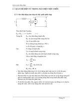
REGISTER 6-1: EECON1 REGISTER (ADDRESS FA6h)
R/W-x R/W-x U-0 R/W-0 R/W-x R/W-0 R/S-0 R/S-0
EEPGD CFGS — FREE WRERR WREN WR RD
bit 7 bit 0
bit 7 EEPGD: FLASH Program or Data EEPROM Memory Select bit
1 = Access FLASH Program memory
0 = Access Data EEPROM memory
bit 6 CFGS: FLASH Program/Data EE or Configuration Select bit
1 = Access Configuration or Calibration registers
0 = Access FLASH Program or Data EEPROM memory
bit 5 Unimplemented: Read as '0'
bit 4 FREE: FLASH Row Erase Enable bit
1 = Erase the program memory row addressed by TBLPTR on the next WR command
(cleared by completion of erase operation)
0 = Perform write only
bit 3 WRERR: FLASH Program/Data EE Error Flag bit
1 = A write operation is prematurely terminated
(any MCLR
or any WDT Reset during self-timed programming in normal operation)
0 = The write operation completed
Note: When a WRERR occurs, the EEPGD or FREE bits are not cleared. This allows tracing
of the error condition.
bit 2 WREN: FLASH Program/Data EE Write Enable bit
1 = Allows write cycles
0 = Inhibits write to the EEPROM
bit 1 WR: Write Control bit
1 = Initiates a data EEPROM erase/write cycle or a program memory erase cycle or write cycle.
(The operation is self-timed and the bit is cleared by hardware once write is complete. The
WR bit can only be set (not cleared) in software.)
0 = Write cycle to the EEPROM is complete
bit 0 RD: Read Control bit
1 = Initiates an EEPROM read
(Read takes one cycle. RD is cleared in hardware. The RD bit can only be set (not cleared)
in software. RD bit cannot be set when EEPGD = 1.)
0 = Does not initiate an EEPROM read
Legend:
R = Readable bit W = Writable bit U = Unimplemented bit, read as ‘0’
- n = Value at POR ’1’ = Bit is set ’0’ = Bit is cleared x = Bit is unknown
© 2006 Microchip Technology Inc. DS39564C-page 67
PIC18FXX2
6.3 Reading the Data EEPROM
Memory
To read a data memory location, the user must write the
address to the EEADR register, clear the EEPGD con-
trol bit (EECON1<7>), clear the CFGS control bit
(EECON1<6>), and then set control bit RD
(EECON1<0>). The data is available for the very next
instruction cycle; therefore, the EEDATA register can
be read by the next instruction. EEDATA will hold this
value until another read operation, or until it is written to
by the user (during a write operation).
EXAMPLE 6-1: DATA EEPROM READ
6.4 Writing to the Data EEPROM
Memory
To write an EEPROM data location, the address must
first be written to the EEADR register and the data writ-
ten to the EEDATA register. Then the sequence in
Example 6-2 must be followed to initiate the write cycle.
The write will not initiate if the above sequence is not
exactly followed (write 55h to EECON2, write AAh to
EECON2, then set WR bit) for each byte. It is strongly
recommended that interrupts be disabled during this
code segment.
Additionally, the WREN bit in EECON1 must be set to
enable writes. This mechanism prevents accidental
writes to data EEPROM due to unexpected code exe-
cution (i.e., runaway programs). The WREN bit should
be kept clear at all times, except when updating the
EEPROM. The WREN bit is not cleared by hardware.
After a write sequence has been initiated, EECON1,
EEADR and EDATA cannot be modified. The WR bit
will be inhibited from being set unless the WREN bit is
set. The WREN bit must be set on a previous instruc-
tion. Both WR and WREN cannot be set with the same
instruction.
At the completion of the write cycle, the WR bit is
cleared in hardware and the EEPROM Write Complete
Interrupt Flag bit (EEIF) is set. The user may either
enable this interrupt, or poll this bit. EEIF must be
cleared by software.
EXAMPLE 6-2: DATA EEPROM WRITE
MOVLW DATA_EE_ADDR ;
MOVWF EEADR ; Data Memory Address to read
BCF EECON1, EEPGD ; Point to DATA memory
BCF EECON1, CFGS ; Access program FLASH or Data EEPROM memory
BSF EECON1, RD ; EEPROM Read
MOVF EEDATA, W ; W = EEDATA
MOVLW DATA_EE_ADDR ;
MOVWF EEADR ; Data Memory Address to read
MOVLW DATA_EE_DATA ;
MOVWF EEDATA ; Data Memory Value to write
BCF EECON1, EEPGD ; Point to DATA memory
BCF EECON1, CFGS ; Access program FLASH or Data EEPROM memory
BSF EECON1, WREN ; Enable writes
BCF INTCON, GIE ; Disable interrupts
Required MOVLW 55h ;
Sequence MOVWF EECON2 ; Write 55h
MOVLW AAh ;
MOVWF EECON2 ; Write AAh
BSF EECON1, WR ; Set WR bit to begin write
BSF INTCON, GIE ; Enable interrupts
. ; user code execution
.
.
BCF EECON1, WREN ; Disable writes on write complete (EEIF set)
PIC18FXX2
DS39564C-page 68 © 2006 Microchip Technology Inc.
6.5 Write Verify
Depending on the application, good programming
practice may dictate that the value written to the mem-
ory should be verified against the original value. This
should be used in applications where excessive writes
can stress bits near the specification limit.
6.6 Protection Against Spurious Write
There are conditions when the device may not want to
write to the data EEPROM memory. To protect against
spurious EEPROM writes, various mechanisms have
been built-in. On power-up, the WREN bit is cleared.
Also, the Power-up Timer (72 ms duration) prevents
EEPROM write.
The write initiate sequence and the WREN bit together
help prevent an accidental write during brown-out,
power glitch, or software malfunction.
6.7 Operation During Code Protect
Data EEPROM memory has its own code protect
mechanism. External Read and Write operations are
disabled if either of these mechanisms are enabled.
The microcontroller itself can both read and write to the
internal Data EEPROM, regardless of the state of the
code protect configuration bit. Refer to “Special Features
of the CPU” (Section 19.0) for additional information.
6.8 Using the Data EEPROM
The data EEPROM is a high endurance, byte address-
able array that has been optimized for the storage of
frequently changing information (e.g., program vari-
ables or other data that are updated often). Frequently
changing values will typically be updated more often
than specification D124. If this is not the case, an array
refresh must be performed. For this reason, variables
that change infrequently (such as constants, IDs, cali-
bration, etc.) should be stored in FLASH program
memory.
A simple data EEPROM refresh routine is shown in
Example 6-3.
EXAMPLE 6-3: DATA EEPROM REFRESH ROUTINE
Note: If data EEPROM is only used to store con-
stants and/or data that changes rarely, an
array refresh is likely not required. See
specification D124.
clrf EEADR ; Start at address 0
bcf EECON1,CFGS ; Set for memory
bcf EECON1,EEPGD ; Set for Data EEPROM
bcf INTCON,GIE ; Disable interrupts
bsf EECON1,WREN ; Enable writes
Loop ; Loop to refresh array
bsf EECON1,RD ; Read current address
movlw 55h ;
movwf EECON2 ; Write 55h
movlw AAh ;
movwf EECON2 ; Write AAh
bsf EECON1,WR ; Set WR bit to begin write
btfsc EECON1,WR ; Wait for write to complete
bra $-2
incfsz EEADR,F ; Increment address
bra Loop ; Not zero, do it again
bcf EECON1,WREN ; Disable writes
bsf INTCON,GIE ; Enable interrupts
© 2006 Microchip Technology Inc. DS39564C-page 69
PIC18FXX2
TABLE 6-1: REGISTERS ASSOCIATED WITH DATA EEPROM MEMORY
Address Name Bit 7 Bit 6 Bit 5 Bit 4 Bit 3 Bit 2 Bit 1 Bit 0
Value on:
POR, BOR
Value on
All Other
RESETS
FF2h INTCON GIE/
GIEH
PEIE/
GIEL
T0IE INTE RBIE T0IF INTF RBIF 0000 000x 0000 000u
FA9h EEADR EEPROM Address Register 0000 0000 0000 0000
FA8h EEDATA EEPROM Data Register 0000 0000 0000 0000
FA7h EECON2 EEPROM Control Register2 (not a physical register) — —
FA6h EECON1 EEPGD CFGS — FREE WRERR WREN WR
RD xx-0 x000 uu-0 u000
FA2h IPR2
— — — EEIP BCLIP LVDIP TMR3IP CCP2IP 1 1111 1 1111
FA1h PIR2
— — —EEIFBCLIF LVDIF TMR3IF CCP2IF 0 0000 0 0000
FA0h PIE2
— — — EEIE BCLIE LVDIE TMR3IE CCP2IE 0 0000 0 0000
Legend: x = unknown, u = unchanged, r = reserved, - = unimplemented, read as '0'.
Shaded cells are not used during FLASH/EEPROM access.
PIC18FXX2
DS39564C-page 70 © 2006 Microchip Technology Inc.
NOTES:
© 2006 Microchip Technology Inc. DS39564C-page 71
PIC18FXX2
7.0 8 X 8 HARDWARE MULTIPLIER
7.1 Introduction
An 8 x 8 hardware multiplier is included in the ALU of
the PIC18FXX2 devices. By making the multiply a
hardware operation, it completes in a single instruction
cycle. This is an unsigned multiply that gives a 16-bit
result. The result is stored into the 16-bit product regis-
ter pair (PRODH:PRODL). The multiplier does not
affect any flags in the ALUSTA register.
Making the 8 x 8 multiplier execute in a single cycle
gives the following advantages:
• Higher computational throughput
• Reduces code size requirements for multiply
algorithms
The performance increase allows the device to be used
in applications previously reserved for Digital Signal
Processors.
Table 7-1 shows a performance comparison between
enhanced devices using the single cycle hardware mul-
tiply, and performing the same function without the
hardware multiply.
TABLE 7-1: PERFORMANCE COMPARISON
7.2 Operation
Example 7-1 shows the sequence to do an 8 x 8
unsigned multiply. Only one instruction is required
when one argument of the multiply is already loaded in
the WREG register.
Example 7-2 shows the sequence to do an 8 x 8 signed
multiply. To account for the sign bits of the arguments,
each argument’s Most Significant bit (MSb) is tested
and the appropriate subtractions are done.
EXAMPLE 7-1: 8 x 8 UNSIGNED
MULTIPLY ROUTINE
EXAMPLE 7-2: 8 x 8 SIGNED MULTIPLY
ROUTINE
Example 7-3 shows the sequence to do a 16 x 16
unsigned multiply. Equation 7-1 shows the algorithm
that is used. The 32-bit result is stored in four registers,
RES3:RES0.
EQUATION 7-1: 16 x 16 UNSIGNED
MULTIPLICATION
ALGORITHM
Routine Multiply Method
Program
Memory
(Words)
Cycles
(Max)
Time
@ 40 MHz @ 10 MHz @ 4 MHz
8 x 8 unsigned
Without hardware multiply 13 69 6.9 μs27.6 μs69 μs
Hardware multiply 1 1 100 ns 400 ns 1 μs
8 x 8 signed
Without hardware multiply 33 91 9.1 μs36.4 μs91 μs
Hardware multiply 6 6 600 ns 2.4 μs6 μs
16 x 16 unsigned
Without hardware multiply 21 242 24.2 μs96.8 μs242 μs
Hardware multiply 24 24 2.4 μs9.6 μs24 μs
16 x 16 signed
Without hardware multiply 52 254 25.4 μs 102.6 μs254 μs
Hardware multiply 36 36 3.6 μs14.4 μs36 μs
MOVF ARG1, W ;
MULWF ARG2 ; ARG1 * ARG2 ->
; PRODH:PRODL
MOVF ARG1, W
MULWF ARG2 ; ARG1 * ARG2 ->
; PRODH:PRODL
BTFSC ARG2, SB ; Test Sign Bit
SUBWF PRODH, F ; PRODH = PRODH
; - ARG1
MOVF ARG2, W
BTFSC ARG1, SB ; Test Sign Bit
SUBWF PRODH, F ; PRODH = PRODH
; - ARG2
RES3:RES0 = ARG1H:ARG1L • ARG2H:ARG2L
= (ARG1H • ARG2H • 2
16
) +
(ARG1H • ARG2L • 2
8
) +
(ARG1L • ARG2H • 2
8
) +
(ARG1L • ARG2L)
PIC18FXX2
DS39564C-page 72 © 2006 Microchip Technology Inc.
EXAMPLE 7-3: 16 x 16 UNSIGNED
MULTIPLY ROUTINE
Example 7-4 shows the sequence to do a 16 x 16
signed multiply. Equation 7-2 shows the algorithm
used. The 32-bit result is stored in four registers,
RES3:RES0. To account for the sign bits of the argu-
ments, each argument pairs Most Significant bit (MSb)
is tested and the appropriate subtractions are done.
EQUATION 7-2: 16 x 16 SIGNED
MULTIPLICATION
ALGORITHM
EXAMPLE 7-4: 16 x 16 SIGNED
MULTIPLY ROUTINE
MOVF ARG1L, W
MULWF ARG2L ; ARG1L * ARG2L ->
; PRODH:PRODL
MOVFF PRODH, RES1 ;
MOVFF PRODL, RES0 ;
;
MOVF ARG1H, W
MULWF ARG2H ; ARG1H * ARG2H ->
; PRODH:PRODL
MOVFF PRODH, RES3 ;
MOVFF PRODL, RES2 ;
;
MOVF ARG1L, W
MULWF ARG2H ; ARG1L * ARG2H ->
; PRODH:PRODL
MOVF PRODL, W ;
ADDWF RES1, F ; Add cross
MOVF PRODH, W ; products
ADDWFC RES2, F ;
CLRF WREG ;
ADDWFC RES3, F ;
;
MOVF ARG1H, W ;
MULWF ARG2L ; ARG1H * ARG2L ->
; PRODH:PRODL
MOVF PRODL, W ;
ADDWF RES1, F ; Add cross
MOVF PRODH, W ; products
ADDWFC RES2, F ;
CLRF WREG ;
ADDWFC RES3, F ;
RES3:RES0
=ARG1H:ARG1L • ARG2H:ARG2L
= (ARG1H • ARG2H • 2
16
) +
(ARG1H • ARG2L • 2
8
) +
(ARG1L • ARG2H • 2
8
) +
(ARG1L • ARG2L) +
(-1 • ARG2H<7> • ARG1H:ARG1L • 2
16
) +
(-1 • ARG1H<7> • ARG2H:ARG2L • 2
16
)
MOVF ARG1L, W
MULWF ARG2L ; ARG1L * ARG2L ->
; PRODH:PRODL
MOVFF PRODH, RES1 ;
MOVFF PRODL, RES0 ;
;
MOVF ARG1H, W
MULWF ARG2H ; ARG1H * ARG2H ->
; PRODH:PRODL
MOVFF PRODH, RES3 ;
MOVFF PRODL, RES2 ;
;
MOVF ARG1L, W
MULWF ARG2H ; ARG1L * ARG2H ->
; PRODH:PRODL
MOVF PRODL, W ;
ADDWF RES1, F ; Add cross
MOVF PRODH, W ; products
ADDWFC RES2, F ;
CLRF WREG ;
ADDWFC RES3, F ;
;
MOVF ARG1H, W ;
MULWF ARG2L ; ARG1H * ARG2L ->
; PRODH:PRODL
MOVF PRODL, W ;
ADDWF RES1, F ; Add cross
MOVF PRODH, W ; products
ADDWFC RES2, F ;
CLRF WREG ;
ADDWFC RES3, F ;
;
BTFSS ARG2H, 7 ; ARG2H:ARG2L neg?
BRA SIGN_ARG1 ; no, check ARG1
MOVF ARG1L, W ;
SUBWF RES2 ;
MOVF ARG1H, W ;
SUBWFB RES3
;
SIGN_ARG1
BTFSS ARG1H, 7 ; ARG1H:ARG1L neg?
BRA CONT_CODE ; no, done
MOVF ARG2L, W ;
SUBWF RES2 ;
MOVF ARG2H, W ;
SUBWFB RES3
;
CONT_CODE
:
© 2006 Microchip Technology Inc. DS39564C-page 73
PIC18FXX2
8.0 INTERRUPTS
The PIC18FXX2 devices have multiple interrupt
sources and an interrupt priority feature that allows
each interrupt source to be assigned a high priority
level or a low priority level. The high priority interrupt
vector is at 000008h and the low priority interrupt vector
is at 000018h. High priority interrupt events will over-
ride any low priority interrupts that may be in progress.
There are ten registers which are used to control
interrupt operation. These registers are:
• RCON
•INTCON
• INTCON2
• INTCON3
• PIR1, PIR2
• PIE1, PIE2
• IPR1, IPR2
It is recommended that the Microchip header files sup-
plied with MPLAB
®
IDE be used for the symbolic bit
names in these registers. This allows the assembler/
compiler to automatically take care of the placement of
these bits within the specified register.
Each interrupt source, except INT0, has three bits to
control its operation. The functions of these bits are:
• Flag bit to indicate that an interrupt event
occurred
• Enable bit that allows program execution to
branch to the interrupt vector address when the
flag bit is set
• Priority bit to select high priority or low priority
The interrupt priority feature is enabled by setting the
IPEN bit (RCON<7>). When interrupt priority is
enabled, there are two bits which enable interrupts glo-
bally. Setting the GIEH bit (INTCON<7>) enables all
interrupts that have the priority bit set. Setting the GIEL
bit (INTCON<6>) enables all interrupts that have the
priority bit cleared. When the interrupt flag, enable bit
and appropriate global interrupt enable bit are set, the
interrupt will vector immediately to address 000008h or
000018h, depending on the priority level. Individual
interrupts can be disabled through their corresponding
enable bits.
When the IPEN bit is cleared (default state), the inter-
rupt priority feature is disabled and interrupts are com-
patible with PICmicro
®
mid-range devices. In
Compatibility mode, the interrupt priority bits for each
source have no effect. INTCON<6> is the PEIE bit,
which enables/disables all peripheral interrupt sources.
INTCON<7> is the GIE bit, which enables/disables all
interrupt sources. All interrupts branch to address
000008h in Compatibility mode.
When an interrupt is responded to, the Global Interrupt
Enable bit is cleared to disable further interrupts. If the
IPEN bit is cleared, this is the GIE bit. If interrupt priority
levels are used, this will be either the GIEH or GIEL bit.
High priority interrupt sources can interrupt a low
priority interrupt.
The return address is pushed onto the stack and the
PC is loaded with the interrupt vector address
(000008h or 000018h). Once in the Interrupt Service
Routine, the source(s) of the interrupt can be deter-
mined by polling the interrupt flag bits. The interrupt
flag bits must be cleared in software before re-enabling
interrupts to avoid recursive interrupts.
The “return from interrupt” instruction, RETFIE, exits
the interrupt routine and sets the GIE bit (GIEH or GIEL
if priority levels are used), which re-enables interrupts.
For external interrupt events, such as the INT pins or
the PORTB input change interrupt, the interrupt latency
will be three to four instruction cycles. The exact
latency is the same for one or two-cycle instructions.
Individual interrupt flag bits are set, regardless of the
status of their corresponding enable bit or the GIE bit.
Note: Do not use the MOVFF instruction to modify
any of the Interrupt control registers while
any interrupt is enabled. Doing so may
cause erratic microcontroller behavior.
PIC18FXX2
DS39564C-page 74 © 2006 Microchip Technology Inc.
FIGURE 8-1: INTERRUPT LOGIC
TMR0IE
GIEH/GIE
GIEL/PEIE
Wake-up if in SLEEP mode
Interrupt to CPU
Vector to location
0008h
INT2IF
INT2IE
INT2IP
INT1IF
INT1IE
INT1IP
TMR0IF
TMR0IE
TMR0IP
RBIF
RBIE
RBIP
IPEN
TMR0IF
TMR0IP
INT1IF
INT1IE
INT1IP
INT2IF
INT2IE
INT2IP
RBIF
RBIE
RBIP
INT0IF
INT0IE
GIEL/PEIE
Interrupt to CPU
Vector to Location
IPEN
IPE
0018h
Peripheral Interrupt Flag bit
Peripheral Interrupt Enable bit
Peripheral Interrupt Priority bit
Peripheral Interrupt Flag bit
Peripheral Interrupt Enable bit
Peripheral Interrupt Priority bit
TMR1IF
TMR1IE
TMR1IP
XXXXIF
XXXXIE
XXXXIP
Additional Peripheral Interrupts
TMR1IF
TMR1IE
TMR1IP
High Priority Interrupt Generation
Low Priority Interrupt Generation
XXXXIF
XXXXIE
XXXXIP
Additional Peripheral Interrupts
GIE/GIEH
© 2006 Microchip Technology Inc. DS39564C-page 75
PIC18FXX2
8.1 INTCON Registers
The INTCON Registers are readable and writable reg-
isters, which contain various enable, priority and flag
bits.
REGISTER 8-1: INTCON REGISTER
Note: Interrupt flag bits are set when an interrupt
condition occurs, regardless of the state of
its corresponding enable bit or the global
enable bit. User software should ensure
the appropriate interrupt flag bits are clear
prior to enabling an interrupt. This feature
allows for software polling.
R/W-0 R/W-0 R/W-0 R/W-0 R/W-0 R/W-0 R/W-0 R/W-x
GIE/GIEH PEIE/GIEL TMR0IE INT0IE RBIE TMR0IF INT0IF RBIF
bit 7 bit 0
bit 7 GIE/GIEH: Global Interrupt Enable bit
When IPEN = 0:
1 = Enables all unmasked interrupts
0 = Disables all interrupts
When IPEN = 1:
1 = Enables all high priority interrupts
0 = Disables all interrupts
bit 6 PEIE/GIEL: Peripheral Interrupt Enable bit
When IPEN = 0:
1 = Enables all unmasked peripheral interrupts
0 = Disables all peripheral interrupts
When IPEN = 1:
1 = Enables all low priority peripheral interrupts
0 = Disables all low priority peripheral interrupts
bit 5 TMR0IE: TMR0 Overflow Interrupt Enable bit
1 = Enables the TMR0 overflow interrupt
0 = Disables the TMR0 overflow interrupt
bit 4 INT0IE: INT0 External Interrupt Enable bit
1 = Enables the INT0 external interrupt
0 = Disables the INT0 external interrupt
bit 3 RBIE: RB Port Change Interrupt Enable bit
1 = Enables the RB port change interrupt
0 = Disables the RB port change interrupt
bit 2 TMR0IF: TMR0 Overflow Interrupt Flag bit
1 = TMR0 register has overflowed (must be cleared in software)
0 = TMR0 register did not overflow
bit 1 INT0IF: INT0 External Interrupt Flag bit
1 = The INT0 external interrupt occurred (must be cleared in software)
0 = The INT0 external interrupt did not occur
bit 0 RBIF: RB Port Change Interrupt Flag bit
1 = At least one of the RB7:RB4 pins changed state (must be cleared in software)
0 = None of the RB7:RB4 pins have changed state
Note: A mismatch condition will continue to set this bit. Reading PORTB will end the
mismatch condition and allow the bit to be cleared.
Legend:
R = Readable bit W = Writable bit U = Unimplemented bit, read as ‘0’
- n = Value at POR ’1’ = Bit is set ’0’ = Bit is cleared x = Bit is unknown
PIC18FXX2
DS39564C-page 76 © 2006 Microchip Technology Inc.
REGISTER 8-2: INTCON2 REGISTER
R/W-1 R/W-1 R/W-1 R/W-1 U-0 R/W-1 U-0 R/W-1
RBPU INTEDG0 INTEDG1 INTEDG2 —TMR0IP—RBIP
bit 7 bit 0
bit 7 RBPU
: PORTB Pull-up Enable bit
1 = All PORTB pull-ups are disabled
0 = PORTB pull-ups are enabled by individual port latch values
bit 6 INTEDG0:External Interrupt0 Edge Select bit
1 = Interrupt on rising edge
0 = Interrupt on falling edge
bit 5 INTEDG1: External Interrupt1 Edge Select bit
1 = Interrupt on rising edge
0 = Interrupt on falling edge
bit 4 INTEDG2: External Interrupt2 Edge Select bit
1 = Interrupt on rising edge
0 = Interrupt on falling edge
bit 3 Unimplemented: Read as '0'
bit 2 TMR0IP: TMR0 Overflow Interrupt Priority bit
1 = High priority
0 = Low priority
bit 1 Unimplemented: Read as '0'
bit 0 RBIP: RB Port Change Interrupt Priority bit
1 = High priority
0 = Low priority
Legend:
R = Readable bit W = Writable bit U = Unimplemented bit, read as ‘0’
- n = Value at POR ’1’ = Bit is set ’0’ = Bit is cleared x = Bit is unknown
Note: Interrupt flag bits are set when an interrupt condition occurs, regardless of the state
of its corresponding enable bit or the global enable bit. User software should ensure
the appropriate interrupt flag bits are clear prior to enabling an interrupt. This feature
allows for software polling.
© 2006 Microchip Technology Inc. DS39564C-page 77
PIC18FXX2
REGISTER 8-3: INTCON3 REGISTER
R/W-1 R/W-1 U-0 R/W-0 R/W-0 U-0 R/W-0 R/W-0
INT2IP INT1IP — INT2IE INT1IE — INT2IF INT1IF
bit 7 bit 0
bit 7 INT2IP: INT2 External Interrupt Priority bit
1 = High priority
0 = Low priority
bit 6 INT1IP: INT1 External Interrupt Priority bit
1 = High priority
0 = Low priority
bit 5 Unimplemented: Read as '0'
bit 4 INT2IE: INT2 External Interrupt Enable bit
1 = Enables the INT2 external interrupt
0 = Disables the INT2 external interrupt
bit 3 INT1IE: INT1 External Interrupt Enable bit
1 = Enables the INT1 external interrupt
0 = Disables the INT1 external interrupt
bit 2 Unimplemented: Read as '0'
bit 1 INT2IF: INT2 External Interrupt Flag bit
1 = The INT2 external interrupt occurred (must be cleared in software)
0 = The INT2 external interrupt did not occur
bit 0 INT1IF: INT1 External Interrupt Flag bit
1 = The INT1 external interrupt occurred (must be cleared in software)
0 = The INT1 external interrupt did not occur
Legend:
R = Readable bit W = Writable bit U = Unimplemented bit, read as ‘0’
- n = Value at POR ’1’ = Bit is set ’0’ = Bit is cleared x = Bit is unknown
Note: Interrupt flag bits are set when an interrupt condition occurs, regardless of the state
of its corresponding enable bit or the global enable bit. User software should ensure
the appropriate interrupt flag bits are clear prior to enabling an interrupt. This feature
allows for software polling.
PIC18FXX2
DS39564C-page 78 © 2006 Microchip Technology Inc.
8.2 PIR Registers
The PIR registers contain the individual flag bits for the
peripheral interrupts. Due to the number of peripheral
interrupt sources, there are two Peripheral Interrupt
Flag Registers (PIR1, PIR2).
REGISTER 8-4: PIR1: PERIPHERAL INTERRUPT REQUEST (FLAG) REGISTER 1
Note 1: Interrupt flag bits are set when an interrupt
condition occurs, regardless of the state of
its corresponding enable bit or the global
enable bit, GIE (INTCON<7>).
2: User software should ensure the appropriate
interrupt flag bits are cleared prior to enabling
an interrupt, and after servicing that interrupt.
R/W-0 R/W-0 R-0 R-0 R/W-0 R/W-0 R/W-0 R/W-0
PSPIF
(1)
ADIF RCIF TXIF SSPIF CCP1IF TMR2IF TMR1IF
bit 7 bit 0
bit 7 PSPIF
(1)
: Parallel Slave Port Read/Write Interrupt Flag bit
1 = A read or a write operation has taken place (must be cleared in software)
0 = No read or write has occurred
bit 6 ADIF: A/D Converter Interrupt Flag bit
1 = An A/D conversion completed (must be cleared in software)
0 = The A/D conversion is not complete
bit 5 RCIF: USART Receive Interrupt Flag bit
1 = The USART receive buffer, RCREG, is full (cleared when RCREG is read)
0 = The USART receive buffer is empty
bit 4 TXIF: USART Transmit Interrupt Flag bit (see Section 16.0 for details on TXIF functionality)
1 = The USART transmit buffer, TXREG, is empty (cleared when TXREG is written)
0 = The USART transmit buffer is full
bit 3 SSPIF: Master Synchronous Serial Port Interrupt Flag bit
1 = The transmission/reception is complete (must be cleared in software)
0 = Waiting to transmit/receive
bit 2 CCP1IF: CCP1 Interrupt Flag bit
Capture mode:
1 = A TMR1 register capture occurred (must be cleared in software)
0 = No TMR1 register capture occurred
Compare mode:
1 = A TMR1 register compare match occurred (must be cleared in software)
0 = No TMR1 register compare match occurred
PWM mode:
Unused in this mode
bit 1 TMR2IF: TMR2 to PR2 Match Interrupt Flag bit
1 = TMR2 to PR2 match occurred (must be cleared in software)
0 = No TMR2 to PR2 match occurred
bit 0 TMR1IF: TMR1 Overflow Interrupt Flag bit
1 = TMR1 register overflowed (must be cleared in software)
0 = MR1 register did not overflow
Note 1: This bit is reserved on PIC18F2X2 devices; always maintain this bit clear.
Legend:
R = Readable bit W = Writable bit U = Unimplemented bit, read as ‘0’
- n = Value at POR ’1’ = Bit is set ’0’ = Bit is cleared x = Bit is unknown
© 2006 Microchip Technology Inc. DS39564C-page 79
PIC18FXX2
REGISTER 8-5: PIR2: PERIPHERAL INTERRUPT REQUEST (FLAG) REGISTER 2
U-0 U-0 U-0 R/W-0 R/W-0 R/W-0 R/W-0 R/W-0
— — — EEIF BCLIF LVDIF TMR3IF CCP2IF
bit 7 bit 0
bit 7-5 Unimplemented: Read as '0'
bit 4 EEIF: Data EEPROM/FLASH Write Operation Interrupt Flag bit
1 = The Write operation is complete (must be cleared in software)
0 = The Write operation is not complete, or has not been started
bit 3 BCLIF: Bus Collision Interrupt Flag bit
1 = A bus collision occurred (must be cleared in software)
0 = No bus collision occurred
bit 2 LVDIF: Low Voltage Detect Interrupt Flag bit
1 = A low voltage condition occurred (must be cleared in software)
0 = The device voltage is above the Low Voltage Detect trip point
bit 1 TMR3IF: TMR3 Overflow Interrupt Flag bit
1 = TMR3 register overflowed (must be cleared in software)
0 = TMR3 register did not overflow
bit 0 CCP2IF: CCPx Interrupt Flag bit
Capture mode:
1 = A TMR1 register capture occurred (must be cleared in software)
0 = No TMR1 register capture occurred
Compare mode:
1 = A TMR1 register compare match occurred (must be cleared in software)
0 = No TMR1 register compare match occurred
PWM mode:
Unused in this mode
Legend:
R = Readable bit W = Writable bit U = Unimplemented bit, read as ‘0’
- n = Value at POR ’1’ = Bit is set ’0’ = Bit is cleared x = Bit is unknown
PIC18FXX2
DS39564C-page 80 © 2006 Microchip Technology Inc.
8.3 PIE Registers
The PIE registers contain the individual enable bits for
the peripheral interrupts. Due to the number of periph-
eral interrupt sources, there are two Peripheral Inter-
rupt Enable Registers (PIE1, PIE2). When IPEN = 0,
the PEIE bit must be set to enable any of these
peripheral interrupts.
REGISTER 8-6: PIE1: PERIPHERAL INTERRUPT ENABLE REGISTER 1
R/W-0 R/W-0 R/W-0 R/W-0 R/W-0 R/W-0 R/W-0 R/W-0
PSPIE
(1)
ADIE RCIE TXIE SSPIE CCP1IE TMR2IE TMR1IE
bit 7 bit 0
bit 7 PSPIE
(1)
: Parallel Slave Port Read/Write Interrupt Enable bit
1 = Enables the PSP read/write interrupt
0 = Disables the PSP read/write interrupt
bit 6 ADIE: A/D Converter Interrupt Enable bit
1 = Enables the A/D interrupt
0 = Disables the A/D interrupt
bit 5 RCIE: USART Receive Interrupt Enable bit
1 = Enables the USART receive interrupt
0 = Disables the USART receive interrupt
bit 4 TXIE: USART Transmit Interrupt Enable bit
1 = Enables the USART transmit interrupt
0 = Disables the USART transmit interrupt
bit 3 SSPIE: Master Synchronous Serial Port Interrupt Enable bit
1 = Enables the MSSP interrupt
0 = Disables the MSSP interrupt
bit 2 CCP1IE: CCP1 Interrupt Enable bit
1 = Enables the CCP1 interrupt
0 = Disables the CCP1 interrupt
bit 1 TMR2IE: TMR2 to PR2 Match Interrupt Enable bit
1 = Enables the TMR2 to PR2 match interrupt
0 = Disables the TMR2 to PR2 match interrupt
bit 0 TMR1IE: TMR1 Overflow Interrupt Enable bit
1 = Enables the TMR1 overflow interrupt
0 = Disables the TMR1 overflow interrupt
Note 1: This bit is reserved on PIC18F2X2 devices; always maintain this bit clear.
Legend:
R = Readable bit W = Writable bit U = Unimplemented bit, read as ‘0’
- n = Value at POR ’1’ = Bit is set ’0’ = Bit is cleared x = Bit is unknown
© 2006 Microchip Technology Inc. DS39564C-page 81
PIC18FXX2
REGISTER 8-7: PIE2: PERIPHERAL INTERRUPT ENABLE REGISTER 2
U-0 U-0 U-0 R/W-0 R/W-0 R/W-0 R/W-0 R/W-0
— — — EEIE BCLIE LVDIE TMR3IE CCP2IE
bit 7 bit 0
bit 7-5 Unimplemented: Read as '0'
bit 4 EEIE: Data EEPROM/FLASH Write Operation Interrupt Enable bit
1 = Enabled
0 = Disabled
bit 3 BCLIE: Bus Collision Interrupt Enable bit
1 = Enabled
0 = Disabled
bit 2 LVDIE: Low Voltage Detect Interrupt Enable bit
1 = Enabled
0 = Disabled
bit 1 TMR3IE: TMR3 Overflow Interrupt Enable bit
1 = Enables the TMR3 overflow interrupt
0 = Disables the TMR3 overflow interrupt
bit 0 CCP2IE: CCP2 Interrupt Enable bit
1 = Enables the CCP2 interrupt
0 = Disables the CCP2 interrupt
Legend:
R = Readable bit W = Writable bit U = Unimplemented bit, read as ‘0’
- n = Value at POR ’1’ = Bit is set ’0’ = Bit is cleared x = Bit is unknown
PIC18FXX2
DS39564C-page 82 © 2006 Microchip Technology Inc.
8.4 IPR Registers
The IPR registers contain the individual priority bits for
the peripheral interrupts. Due to the number of periph-
eral interrupt sources, there are two Peripheral Inter-
rupt Priority Registers (IPR1, IPR2). The operation of
the priority bits requires that the Interrupt Priority
Enable (IPEN) bit be set.
REGISTER 8-8: IPR1: PERIPHERAL INTERRUPT PRIORITY REGISTER 1
R/W-1 R/W-1 R/W-1 R/W-1 R/W-1 R/W-1 R/W-1 R/W-1
PSPIP
(1)
ADIP RCIP TXIP SSPIP CCP1IP TMR2IP TMR1IP
bit 7 bit 0
bit 7 PSPIP
(1)
: Parallel Slave Port Read/Write Interrupt Priority bit
1 = High priority
0 = Low priority
bit 6 ADIP: A/D Converter Interrupt Priority bit
1 = High priority
0 = Low priority
bit 5 RCIP: USART Receive Interrupt Priority bit
1 = High priority
0 = Low priority
bit 4 TXIP: USART Transmit Interrupt Priority bit
1 = High priority
0 = Low priority
bit 3 SSPIP: Master Synchronous Serial Port Interrupt Priority bit
1 = High priority
0 = Low priority
bit 2 CCP1IP: CCP1 Interrupt Priority bit
1 = High priority
0 = Low priority
bit 1 TMR2IP: TMR2 to PR2 Match Interrupt Priority bit
1 = High priority
0 = Low priority
bit 0 TMR1IP: TMR1 Overflow Interrupt Priority bit
1 = High priority
0 = Low priority
Note 1: This bit is reserved on PIC18F2X2 devices; always maintain this bit set.
Legend:
R = Readable bit W = Writable bit U = Unimplemented bit, read as ‘0’
- n = Value at POR ’1’ = Bit is set ’0’ = Bit is cleared x = Bit is unknown
© 2006 Microchip Technology Inc. DS39564C-page 83
PIC18FXX2
REGISTER 8-9: IPR2: PERIPHERAL INTERRUPT PRIORITY REGISTER 2
U-0 U-0 U-0 R/W-1 R/W-1 R/W-1 R/W-1 R/W-1
— — — EEIP BCLIP LVDIP TMR3IP CCP2IP
bit 7 bit 0
bit 7-5 Unimplemented: Read as '0'
bit 4 EEIP: Data EEPROM/FLASH Write Operation Interrupt Priority bit
1 = High priority
0 = Low priority
bit 3 BCLIP: Bus Collision Interrupt Priority bit
1 = High priority
0 = Low priority
bit 2 LVDIP: Low Voltage Detect Interrupt Priority bit
1 = High priority
0 = Low priority
bit 1 TMR3IP: TMR3 Overflow Interrupt Priority bit
1 = High priority
0 = Low priority
bit 0 CCP2IP: CCP2 Interrupt Priority bit
1 = High priority
0 = Low priority
Legend:
R = Readable bit W = Writable bit U = Unimplemented bit, read as ‘0’
- n = Value at POR ’1’ = Bit is set ’0’ = Bit is cleared x = Bit is unknown
PIC18FXX2
DS39564C-page 84 © 2006 Microchip Technology Inc.
8.5 RCON Register
The RCON register contains the bit which is used to
enable prioritized interrupts (IPEN).
REGISTER 8-10: RCON REGISTER
R/W-0 U-0 U-0 R/W-1 R-1 R-1 R/W-0 R/W-0
IPEN
— —RITO PD POR BOR
bit 7 bit 0
bit 7 IPEN: Interrupt Priority Enable bit
1 = Enable priority levels on interrupts
0 = Disable priority levels on interrupts (16CXXX Compatibility mode)
bit 6-5 Unimplemented: Read as '0'
bit 4 RI
: RESET Instruction Flag bit
For details of bit operation, see Register 4-3
bit 3 TO: Watchdog Time-out Flag bit
For details of bit operation, see Register 4-3
bit 2 PD: Power-down Detection Flag bit
For details of bit operation, see Register 4-3
bit 1 POR: Power-on Reset Status bit
For details of bit operation, see Register 4-3
bit 0 BOR: Brown-out Reset Status bit
For details of bit operation, see Register 4-3
Legend:
R = Readable bit W = Writable bit U = Unimplemented bit, read as ‘0’
- n = Value at POR ’1’ = Bit is set ’0’ = Bit is cleared x = Bit is unknown
© 2006 Microchip Technology Inc. DS39564C-page 85
PIC18FXX2
8.6 INT0 Interrupt
External interrupts on the RB0/INT0, RB1/INT1 and
RB2/INT2 pins are edge triggered: either rising, if the
corresponding INTEDGx bit is set in the INTCON2 reg-
ister, or falling, if the INTEDGx bit is clear. When a valid
edge appears on the RBx/INTx pin, the corresponding
flag bit INTxF is set. This interrupt can be disabled by
clearing the corresponding enable bit INTxE. Flag bit
INTxF must be cleared in software in the Interrupt Ser-
vice Routine before re-enabling the interrupt. All exter-
nal interrupts (INT0, INT1 and INT2) can wake-up the
processor from SLEEP, if bit INTxE was set prior to
going into SLEEP. If the global interrupt enable bit GIE
is set, the processor will branch to the interrupt vector
following wake-up.
Interrupt priority for INT1 and INT2 is determined by the
value contained in the interrupt priority bits, INT1IP
(INTCON3<6>) and INT2IP (INTCON3<7>). There is
no priority bit associated with INT0. It is always a high
priority interrupt source.
8.7 TMR0 Interrupt
In 8-bit mode (which is the default), an overflow
(FFh → 00h) in the TMR0 register will set flag bit
TMR0IF. In 16-bit mode, an overflow (FFFFh → 0000h)
in the TMR0H:TMR0L registers will set flag bit TMR0IF.
The interrupt can be enabled/disabled by setting/
clearing enable bit T0IE (INTCON<5>). Interrupt prior-
ity for Timer0 is determined by the value contained in
the interrupt priority bit TMR0IP (INTCON2<2>). See
Section 10.0 for further details on the Timer0 module.
8.8 PORTB Interrupt-on-Change
An input change on PORTB<7:4> sets flag bit RBIF
(INTCON<0>). The interrupt can be enabled/disabled
by setting/clearing enable bit, RBIE (INTCON<3>).
Interrupt priority for PORTB interrupt-on-change is
determined by the value contained in the interrupt
priority bit, RBIP (INTCON2<0>).
8.9 Context Saving During Interrupts
During an interrupt, the return PC value is saved on the
stack. Additionally, the WREG, STATUS and BSR regis-
ters are saved on the fast return stack. If a fast return
from interrupt is not used (See Section 4.3), the user
may need to save the WREG, STATUS and BSR regis-
ters in software. Depending on the user’s application,
other registers may also need to be saved. Equation 8-1
saves and restores the WREG, STATUS and BSR
registers during an Interrupt Service Routine.
EXAMPLE 8-1: SAVING STATUS, WREG AND BSR REGISTERS IN RAM
MOVWF W_TEMP ; W_TEMP is in virtual bank
MOVFF STATUS, STATUS_TEMP ; STATUS_TEMP located anywhere
MOVFF BSR, BSR_TEMP ; BSR located anywhere
;
; USER ISR CODE
;
MOVFF BSR_TEMP, BSR ; Restore BSR
MOVF W_TEMP, W ; Restore WREG
MOVFF STATUS_TEMP,STATUS ; Restore STATUS
PIC18FXX2
DS39564C-page 86 © 2006 Microchip Technology Inc.
NOTES:
© 2006 Microchip Technology Inc. DS39564C-page 87
PIC18FXX2
9.0 I/O PORTS
Depending on the device selected, there are either five
ports or three ports available. Some pins of the I/O
ports are multiplexed with an alternate function from
the peripheral features on the device. In general, when
a peripheral is enabled, that pin may not be used as a
general purpose I/O pin.
Each port has three registers for its operation. These
registers are:
• TRIS register (data direction register)
• PORT register (reads the levels on the pins of the
device)
• LAT register (output latch)
The data latch (LAT register) is useful for read-modify-
write operations on the value that the I/O pins are
driving.
9.1 PORTA, TRISA and LATA
Registers
PORTA is a 7-bit wide, bi-directional port. The corre-
sponding Data Direction register is TRISA. Setting a
TRISA bit (= 1) will make the corresponding PORTA pin
an input (i.e., put the corresponding output driver in a
Hi-Impedance mode). Clearing a TRISA bit (= 0) will
make the corresponding PORTA pin an output (i.e., put
the contents of the output latch on the selected pin).
Reading the PORTA register reads the status of the
pins, whereas writing to it will write to the port latch.
The Data Latch register (LATA) is also memory
mapped. Read-modify-write operations on the LATA
register reads and writes the latched output value for
PORTA.
The RA4 pin is multiplexed with the Timer0 module
clock input to become the RA4/T0CKI pin. The RA4/
T0CKI pin is a Schmitt Trigger input and an open drain
output. All other RA port pins have TTL input levels and
full CMOS output drivers.
The other PORTA pins are multiplexed with analog
inputs and the analog V
REF+ and VREF- inputs. The
operation of each pin is selected by clearing/setting the
control bits in the ADCON1 register (A/D Control
Register1).
The TRISA register controls the direction of the RA
pins, even when they are being used as analog inputs.
The user must ensure the bits in the TRISA register are
maintained set when using them as analog inputs.
EXAMPLE 9-1: INITIALIZING PORTA
FIGURE 9-1: BLOCK DIAGRAM OF
RA3:RA0 AND RA5 PINS
Note: On a Power-on Reset, RA5 and RA3:RA0
are configured as analog inputs and read
as ‘0’. RA6 and RA4 are configured as
digital inputs.
CLRF PORTA ; Initialize PORTA by
; clearing output
; data latches
CLRF LATA ; Alternate method
; to clear output
; data latches
MOVLW 0x07 ; Configure A/D
MOVWF ADCON1 ; for digital inputs
MOVLW 0xCF ; Value used to
; initialize data
; direction
MOVWF TRISA ; Set RA<3:0> as inputs
; RA<5:4> as outputs
Data
Bus
QD
Q
CK
QD
Q
CK
QD
EN
P
N
WR LATA
WR TRISA
Data Latch
TRIS Latch
RD TRISA
RD PORTA
V
SS
VDD
I/O pin
(1)
Note 1: I/O pins have protection diodes to VDD and VSS.
Analog
Input
Mode
TTL
Input
Buffer
To A/D Converter and LVD Modules
RD LATA
or
PORTA
SS Input (RA5 only)
PIC18FXX2
DS39564C-page 88 © 2006 Microchip Technology Inc.
FIGURE 9-2: BLOCK DIAGRAM OF
RA4/T0CKI PIN
FIGURE 9-3: BLOCK DIAGRAM OF
RA6 PIN
Data
Bus
WR TRISA
RD PORTA
Data Latch
TRIS Latch
RD TRISA
Schmitt
Trigger
Input
Buffer
N
V
SS
I/O pin
(1)
TMR0 Clock Input
QD
Q
CK
QD
Q
CK
EN
QD
EN
RD LATA
WR LATA
or
PORTA
Note 1: I/O pin has protection diode to V
SS only.
Data
Bus
Q
D
Q
CK
QD
EN
P
N
WR LATA
WR
Data Latch
TRIS Latch
RD TRISA
RD PORTA
V
SS
VDD
I/O pin
(1)
Note 1: I/O pins have protection diodes to VDD and VSS.
or
PORTA
RD LATA
ECRA6 or
ECRA6 or
Enable
TTL
Input
Buffer
RCRA6
RCRA6 Enable
TRISA
Q
D
Q
CK
© 2006 Microchip Technology Inc. DS39564C-page 89
PIC18FXX2
TABLE 9-1: PORTA FUNCTIONS
TABLE 9-2: SUMMARY OF REGISTERS ASSOCIATED WITH PORTA
Name Bit# Buffer Function
RA0/AN0 bit0 TTL Input/output or analog input.
RA1/AN1 bit1 TTL Input/output or analog input.
RA2/AN2/V
REF- bit2 TTL Input/output or analog input or VREF
RA3/AN3/VREF+ bit3 TTL Input/output or analog input or VREF+.
RA4/T0CKI bit4 ST Input/output or external clock input for Timer0.
Output is open drain type.
RA5/SS/
AN4/LVDIN bit5 TTL Input/output or slave select input for synchronous serial port or analog
input, or low voltage detect input.
OSC2/CLKO/RA6 bit6 TTL OSC2 or clock output or I/O pin.
Legend: TTL = TTL input, ST = Schmitt Trigger input
Name Bit 7 Bit 6 Bit 5 Bit 4 Bit 3 Bit 2 Bit 1 Bit 0
Value on
POR,
BOR
Value on
All Other
RESETS
PORTA
— RA6 RA5 RA4 RA3 RA2 RA1 RA0 -x0x 0000 -u0u 0000
LATA
— LATA Data Output Register -xxx xxxx -uuu uuuu
TRISA
— PORTA Data Direction Register -111 1111 -111 1111
ADCON1
ADFM ADCS2 — — PCFG3 PCFG2 PCFG1 PCFG0 00 0000 00 0000
Legend: x = unknown, u = unchanged, - = unimplemented locations read as '0'. Shaded cells are not used by PORTA.
PIC18FXX2
DS39564C-page 90 © 2006 Microchip Technology Inc.
9.2 PORTB, TRISB and LATB
Registers
PORTB is an 8-bit wide, bi-directional port. The corre-
sponding Data Direction register is TRISB. Setting a
TRISB bit (= 1) will make the corresponding PORTB pin
an input (i.e., put the corresponding output driver in a
Hi-Impedance mode). Clearing a TRISB bit (= 0) will
make the corresponding PORTB pin an output (i.e., put
the contents of the output latch on the selected pin).
The Data Latch register (LATB) is also memory
mapped. Read-modify-write operations on the LATB
register reads and writes the latched output value for
PORTB.
EXAMPLE 9-2: INITIALIZING PORTB
Each of the PORTB pins has a weak internal pull-up. A
single control bit can turn on all the pull-ups. This is per-
formed by clearing bit RBPU
(INTCON2<7>). The
weak pull-up is automatically turned off when the port
pin is configured as an output. The pull-ups are
disabled on a Power-on Reset.
Four of the PORTB pins, RB7:RB4, have an interrupt-
on-change feature. Only pins configured as inputs can
cause this interrupt to occur (i.e., any RB7:RB4 pin
configured as an output is excluded from the interrupt-
on-change comparison). The input pins (of RB7:RB4)
are compared with the old value latched on the last
read of PORTB. The “mismatch” outputs of RB7:RB4
are OR’ed together to generate the RB Port Change
Interrupt with flag bit, RBIF (INTCON<0>).
This interrupt can wake the device from SLEEP. The
user, in the Interrupt Service Routine, can clear the
interrupt in the following manner:
a) Any read or write of PORTB (except with the
MOVFF instruction). This will end the mismatch
condition.
b) Clear flag bit RBIF.
A mismatch condition will continue to set flag bit RBIF.
Reading PORTB will end the mismatch condition and
allow flag bit RBIF to be cleared.
The interrupt-on-change feature is recommended for
wake-up on key depression operation and operations
where PORTB is only used for the interrupt-on-change
feature. Polling of PORTB is not recommended while
using the interrupt-on-change feature.
RB3 can be configured by the configuration bit
CCP2MX as the alternate peripheral pin for the CCP2
module (CCP2MX=’0’).
FIGURE 9-4: BLOCK DIAGRAM OF
RB7:RB4 PINS
Note: On a Power-on Reset, these pins are
configured as digital inputs.
CLRF PORTB ; Initialize PORTB by
; clearing output
; data latches
CLRF LATB ; Alternate method
; to clear output
; data latches
MOVLW 0xCF ; Value used to
; initialize data
; direction
MOVWF TRISB ; Set RB<3:0> as inputs
; RB<5:4> as outputs
; RB<7:6> as inputs
Note 1: While in Low Voltage ICSP mode, the
RB5 pin can no longer be used as a gen-
eral purpose I/O pin, and should be held
low during normal operation to protect
against inadvertent ICSP mode entry.
2: When using Low Voltage ICSP program-
ming (LVP), the pull-up on RB5 becomes
disabled. If TRISB bit 5 is cleared,
thereby setting RB5 as an output, LATB
bit 5 must also be cleared for proper
operation.
Data Latch
From other
RBPU
(2)
P
V
DD
I/O pin
(1)
QD
CK
QD
CK
QD
EN
QD
EN
Data Bus
WR LATB
WR TRISB
Set RBIF
TRIS Latch
RD TRISB
RD PORTB
RB7:RB4 pins
Weak
Pull-up
RD PORTB
Latch
TTL
Input
Buffer
ST
Buffer
RB7:RB5 in Serial Programming mode
Q3
Q1
RD LATB
or
PORTB
Note 1: I/O pins have diode protection to V
DD and VSS.
2: To enable weak pull-ups, set the appropriate TRIS bit(s)
and clear the RBPU
bit (INTCON2<7>).