Nanotechnology Global Strategies, Industry Trends and Applications phần 6 docx
Bạn đang xem bản rút gọn của tài liệu. Xem và tải ngay bản đầy đủ của tài liệu tại đây (336.44 KB, 19 trang )
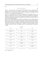
Figure 4.4 Reaching the NNI vision
In FY 2001, NNI identified nine areas of grand challenges (National Science and
Technology Council 2000). Nanobiotechnology and nanobiomedical research has
progressively increas ed in importance (National Institutes of Health 2000). In 2002
three new grand challenges were added, related to manufacturing at the nanoscale,
instrumentation, and chemico-biological-radioactive-explosive detection and
protection. The second strategic planning of NNI has been completed in December
2004 (NSET, 2004) based to the new knowledge and technological foundation
developed in the first four years of NNI (Roco 2004). The long-term vision has been
established first, and then we have determined the requirements for shorter-term
goals and priority themes (Figure 4.4).
Nanoscale manufacturing R&D is an example of a long-term objective of
developing systematic methods for economic synthesis and fabrication of three-
dimensional nanostructures, establishing nanoscale manufacturing capabilities, and
establishing the markets for nanotechnology producers and users. Another impor-
tant challenge is establish ing standardized and reproducible microfabricated
approaches to nanocharacterization, nanomanipulation, and nanodevices.
The centers and networks of excellence encourage long-term, system-oriented
projects, research networking, and shared academic user facilities. These nano-
technology research centers will play an important role in the development and
utilization of specific tools, and in promoting partnerships in the coming years
(Tables 4.3 and 4.4).
NSF will run two user networks – the National Nanotechnology Infrastructure
Network and the Network for Computational Nanotechnology – and twelve
nanoscale science and engineering centers and continue support for thirteen
materials research science and engineering centers with research at the nanoscale.
DOE has established five large-scale user facilities – the Nanoscale Science
Research Centers – NASA four nano-bio-info research centers, DOD three centers,
and NIH several visualization and instrumentation centers.
In planning for the future, NNI has been prepared with the same rigor as a
scientific project, including a long-term vision developed in 1999 (Roco et al. 2000;
National Science and Technology Council 1999, 2000; ). The
National Research Cou ncil (NRC) reviewed NNI in 2002 (National Research
Council 2002), and made a series of recommendations such as increasing R&D
investment on nanobiosystems and societal implications.
Two bills for nanotechnology submitted in 2003 in the US Congress addressed
the need for coherent, multi-year planning with increased interdisciplinarity and
interagency coordination. Senate bill S189, 21st Century Nanotechnology R&D
Act, in the 108th Congress recommends a five-year National Nanotechnology
Program. It was introduced by a group of senators led by Ron Wyden (Democrat,
Oregon) and George Allen (Republican, Virginia). The draft bill in the House was
HR 766, Nanotechnology Research and Development Act of 2003; it was intro-
duced by a group of representatives led by Sherwood Boehlert (Republican, New
York) and Michael Honda (Democrat, California). The two bills were approved by
President Bush in December 2003 along with Public Law 108-153. Societal goals
The US National Nanotechnology Initiative 87
and R&D were discussed at each of the previous Congressional nanotechnology
hearings, including one on 19 March 2003, and a special hearing on this topic was
held on 9 April 2003 by the House Committee on Science. The hearing suggested
the need to increase funding in this area and to involve social scientists from the
beginning in large NNI projects.
Table 4.3 NNI centers and networks of excellence
Institution Year
initiated
NSF
Nanoscale Systems in Information Technologies,
NSEC (Nanoscale Science and Engineering
Center)
Cornell University 2001
Nanoscience in Biological and Environmental
Engineering, NSEC
Rice University 2001
Integrated Nanopatterning and Detection, NSEC Northwestern University 2001
Electronic Transport in Molecular
Nanostructures, NSEC
Columbia University 2001
Nanoscale Systems and Their Device
Applications, NSEC
Harvard University 2001
Directed Assembly of Nanostructures, NSEC Rensselaer Polytechnic Institute 2001
Nanobiotechnology, Science and Technology
Center
Cornell University 2000
Integrated and Scalable Nanomanufacturing,
NSEC
UC Los Angeles 2003
Nanoscale Chemical, Electrical, and Mechanical
Manufacturing Systems, NSEC
UIUC 2003
Integrated Nanomechanical Systems, NSEC UC Berkeley 2004
High Rate Nanomanufacturing, NSEC Northeastern University 2004
Affordable Nanoengineering of Polymer
Biomedical Devices, NSEC
Ohio State University 2004
Nano-bio Interface, NSEC University of Pennsylvania 2004
Probing the Nanoscale, NSEC Stanford University 2004
Templated Synthesis and Assembly at the
Nanoscale, NSEC
University of Wisconsin,
Madison
2004
DOD
Institute for Soldier Nanotechnologies MIT 2002
Center for Nanoscience Innovation for Defense UC Santa Barbara 2002
Nanoscience Institute Naval Research Laboratory 2002
NASA
Institute for Cell Mimetic Space Exploration UCLA 2002
Institute for Intelligent Bio-Nanomaterials and
Structures for Aerospace Vehicles
Texas A&M 2002
Bio-Inspection, Design and Processing of
Multi-functional Nanocomposites
Princeton 2002
Institute for Nanoelectronics and Computing Purdue 2002
88 Nanotechnology
4.3.3 Policy of Inclusion and Partnerships, Including Promoting
Interagency Collaboration
This strategy applies to various disciplines, areas of relevance, research providers
and users, technology and societal aspects, and international integration. The vision
of a ‘grand coalition’ of collaborating universities, industry, government labora-
tories, government agencies, and professional science and engineering communities
was proposed in 1999 (Roco et al. 2000: V–VIII) and has been implemented
through NNI. The added value by synergy in science and technology resulting from
partnerships is one of the main reason of establishing NNI. A starting point was the
collaborations and monthly working meetings of currently 21 federal agencies
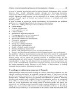
covering almost all relevant areas of nanotechnology (Figure 4.5).
Coordination between agencies is a key task of the NSTC’s Subcommittee on
Nanoscale Science, Engineering and Technology (NSET). It coordinates planning
and budgets of the participating agencies, identifies promising research directions,
encourages collaborative investments, avoids duplication of effort, and ensures
development of a balanced infrastructure. The National Nanotechnology Coordi-
nating Office (NNCO) serves as secretariat to NSET providing technical and
administrative support to implement the interagency activities and prepare planning
and assessment documents. For example, NSET has coordinated the establishment
of new centers and facilities with complementary functions that are being devel-
oped by the different agencies.
In addition to industry, an increased role of states and universities in funding
nanotechnology has been evident in the US since 2002. Examples are the states of
New York (the Albany Nanotechnology Center), California (the California Nan o-
systems Institute with additional matching from industry at a ratio of 2:1), Illinois
(the Institute for Nanotechnology, with joint funding from Northwestern University,
Table 4.4 NNI R&D user facilities
Institution Year
initiated
NSF
National Nanotechnology Infrastructure
Network (NNIN): a network of 13
academic facilities
Main node at Cornell University 2004
Network for Computational Nanotechnology
(NCN): a network of 7 academic facilities
Main node at Purdue University 2004
DOE
Center for Functional Nanomaterials Brookhaven National Laboratory
Center for Integrated Nanotechnologies SNL and LANL
Center for Nanophase Materials Sciences Oak Ridge National Laboratory
Center for Nanoscale Materials Argonne National Laboratory
Molecular Foundry Lawrence Berkeley National
Laboratory
The US National Nanotechnology Initiative 89
and the Center for Nanofabrication and Molecular Self-assembly, with other
funding agencies), Pennsylvania (the Franklin Institute for developing partnerships
in nanotechnology) , Georgia (a new center) and Indiana (contributions to the
nanotechnology investment at Purdue University). It is estimated that US industry
made about the same level of investment in nanoscale science and engineering
research as the federal government in 2003, but it is generally directed to ‘vertical’
transformations of a fundamental discovery into a product, whereas the federal
investment is generally directed to ‘horizontal’ basic discoveries of relevance to
multiple disciplines and areas of relevance. International collaborations are part of
the overall partnershi ps and they are increasing in importance.
4.3.4 Preparation of a Diverse Nanotechnology Workforce
A major challenge is to educate and train a new generation of workers skilled in the
multidisciplinary perspectives necessary for rapid progress in nanotechnology. The
concepts at the nanoscale (atomic, molecular, and supra molecular levels) should
penetrate the education system in the next decade in the same way that microscopic
Figure 4.5 NNI embraces 21 federal departments and independent agencies covering
various societal needs
90 Nanotechnology
approaches made inroads in the past fifty years. NSF has a plan for systemic and
earlier nanoscale science and engineering education. The R&D workforce is
managed using merit review and individual incentives. It is estimated that about
2 million nanotechnology workers will be needed worldwide in 10–15 years. One
way to ensure a pipeline of new students into the field is to promote interaction with
the public at large. Since 2002 several US universities have reported increased
numbers of highly qualified students moving into physical and engineering sciences
because of the NNI.
Timely education and training will begin moving concepts from the microscopic
world to the molecular and supramolecular levels. Changes in teaching from
kindergarten to gradu ate school, as well as continuing education activities for
retraining, are envisioned. An important corollary activity is the retraining of
teachers themselves. One may consider changes in how we structure information on
nanotechnology (Yamaguchi and Komiyama 2001) in order to improve learning
and disseminate the results. Five-year goals for NNI include ensuring that 50%
of research institutions’ faculty and student s have access to the full range of
nanoscale research facilities, and enabling access to nanoscience and engineering
education for students in at least 25% of research universities. Here are three
illustrations:
NSF’s Nanotechnology Undergraduate Education program has made about 70
awards in FY 2003 and FY 2004. Nanotechnology grade 7–12 education has
been funded through a national center at the Northwestern University and an
increased focus on public education is planned in 2005.
In 2004 a coherent plan has been developed to integrate high-school, technolo-
gical, undergraduate, and graduate education into a collaborative environment.
The software NanoKids (Tour 2003) has been developed for interactive learning
using video animation on easily accessible computers (Figure 4.6).
Figure 4.6 NanoKids: interactive teaching software for high school. Reproduced with
permission from Tour (2003)
The US National Nanotechnology Initiative 91
4.3.5 Address Broad Societal Goals
The first report on societal implications of nanoscience and nanotechnology (Roco
and Bainbridge 2001) was prepared at the onset of NNI in September 2000, and its
recommendations were reflected in the NSF program announcements and the opera-
tion of NNCO. Nanoscale science and engineering will lead to better understanding
of nature, economic prosperity, and improved health, sustainability, and peace. This
strategy has strong roots and may bring people and countries together. An integral
aspect of NNI’s broader goals is increasing productivity by applying innovative
nanotechnology for commerce (manufacturing, computing and communications,
power systems, energy). Taking this road towards broader goals may bring large
benefits in the long term. Aiming at broad societal goals was one of the initial stra-
tegies of NNI (Roco 2003), and it has expanded to converging technologies from the
nanoscale for improving human performance (Roco and Bainbridge 2003).
Since October 2000 the annual NSF program announcement has included a focus
on ethical, legal, and societal implications and on workforce education and training.
Research on societal and educational implications will increase in importance as novel
nanostructures are discovered, new nanotechnology products and services reach the
market, and interdisciplinary research groups are established to study them. The NNI
annual investment in research with societal and educational implications in 2004
is estimated at about $45 million (of which NSF awards about $40 million), and
in nanoscale research with relevance to environment and health and safety at about
$90 million (of which NSF awards about $40 million, NIH about $33 million and
EPA about $6 million). The total of about $90 million is approximately 10% of the
NNI budget in FY 2004. One example of a supported project is cleaning
contaminated soil using iron nanoparticles that are partially coated with other
metals (Figure 4.7). This proje ct received joint support from NSF and the
Environmental Protecti on A gency (EPA).
Societal implications include the envisioned benefits from nanotechnology as
well as second-order consequences, such as potential risks, disruptive technologies,
and ethical aspects. Long-term developments of the field depend on the way one
addresses the ‘societal challenges’ of nanotechnology (Lane 2001). NSET is
actively seeking input from research groups, social and economical experts,
professional societies, and industry on this issue.
4.4 Closing Remarks
I would like to close this brief overview of NNI with several comments about
international collaboration in the future. Nanoscale science and engineering R&D is
mostly in a precompetitive phase. International collaboration in fundamental
research, long-te rm technical challenges, metrology, education, and studies on
societal implications will play an important role in the affirmation and growth of the
field. The US NNI develops in this context. The vision-setting and collaborative
model of NNI has received international acceptance.
92 Nanotechnology
Opportunities for collaboration towards an international nanotechnology effort,
particularly in the precompetitive areas, will augment the national programs. One
may note that large companies rely heavily on R&D results from external sources
(about 80% in 2001), of which a large proportion is from other countries (Europe
35%, Japan 33%, US 12%, according to E. Roberts, MIT, at the Sloan School of
Management). An increased number of companies are acting globally with a
significant flow of ideas, capital, and people. This trend will accelerate and will
be the environment in which nanotechnology will develop.
Priority goals may be envisioned for international collaboration in nanoscale
research and education: better comprehension of nature, increased productivity,
sustainable development, and development of humanity and civilization. Examples
include understanding single molecules and the operation of single cells, improving
health and human performance, enhancing simulation and measuring methods,
creating assembly and fabrication tools for the building blocks of matter, and
developing highly efficient solar energy conversion and water desalinization for
sustainable development.
Acknowledgements
Opinions expressed here are those of the author and do not necessarily reflect the
position of NSET or NSF. This chapter is based on a presentation made at the
Figure 4.7 Cleaning the environment with iron nanoparticles. Reproduced with permission
from Zhang (2003)
The US National Nanotechnology Initiative 93
National Nanotechnology Initiative Conference, Infocast, Washington, DC, on
3 April 2003; several items were updated before publication.
References
1. Lane, N. Grand challenges of nanotechnology. Journal of Nanoparticle Research 3(2/3), (2001) 1–8.
2. National Institutes of Health. Nanoscience and Nanotechnology: Shaping Biomedical Research (2000)
NIH, Washington, DC ( or />3. National Research Council. Small Wonders – Endless Frontiers: A Review of the National Nano-
technology Initiative (2002) National Academies Press, Washington, DC.
4. National Science and Technology Council. Nanotechnology – Shaping the World Atom by Atom
(1999) Brochure for the public, NSTC, Washington, DC ().
5. National Science and Technology Council. National Nanotechnology Initiative: The Initiative and
Its Implementation Plan (2000) NSTC, Washington, DC ().
6. National Science and Technology Council, National Nanotechnology Initiative Strategic Plan, Dec.
2004, Washington, D.C. ()
7. Roco, M. C. Broad societal issues of nanotechnology. Journal of Nanoparticle Research 5(3/4), (2003)
181–189.
8. Roco, M. C. The U.S. National Nanotechnology Initiative after 3 years (2001–2003). Journal of
Nanoparticle Research 6(1), (2004) 1–10.
9. Roco, M. C. and Bainbridge, W. (eds). Societal Implications of Nanoscience and Nanotechnology
(2001) NSF and Kluwer, Boston MA.
10. Roco, M. C. and Bainbridge, W. (eds). Converging Technologies for Improving Human Performance
(2003) Kluwer, Boston MA. First published in June 2002 as an NSF-DOC report.
11. Roco, M. C., Williams, R. S. and Alivisatos, P. (eds). Nanotechnology Research Directions (2000)
Kluwer, Boston MA. First published in 1999 as an NSTC report.
12. Siegel, R. W., Hu, E. and Roco, M. C. (eds). Nanostructure Science and Technology (1999) NSTC and
Kluwer, Boston MA.
13. Tour, J. NanoKids. Seminar presented at National Science Foundation, (2003) NSF award 0236281,
Arlington VA.
14. Yamaguchi, Y. and Komiyama, H. Structuring knowledge project in nanotechnology materials
program launched in Japan. Journal of Nanoparticle Research 3(2/3), (2001) 1–5.
15. Zhang, W. Nanoscale iron particles for environmental remediation: an overview. Journal of Nano-
particle Research 5(3/4), (2003) 323–332.
94 Nanotechnology
Part Two
Investing in
Nanotechnology
5
Growth through
Nanotechnology Opportunities
and Risks
Jurgen Schulte
Asia Pacific Nanotechnology Forum
It was not the computer box on the desk itself that triggered the tremendous growth
in the IT industry. There were computers on our desks for about 20 years before a
significant growth in the IT industry was observed. What trigge red that growth was
a sequence of enabling technologies that made it possible to easily collaborate and
communicate beyond the boundaries of the office cubicle. At first, the increasing
data density of hard disks made it possible to store applications which became
increasingly useful to the general office environment. The advent of computer
network technology reduced the cost of communication, and hence collaboration, to
an almost negligible amount of a normal business or household operation. Network
technology as enabling technology behind our desktop and mobile computers has
lifted the computer industry to heights unthought of at the time when the first
computer box revolutionized business operation.
While mainstream computer technology is more or less based around a primary
electronics industry, we see nanotechnology emerging at the core of many indus-
tries. This is easily understood when looking at the nanometer scale, a size scale
of importance to all manufacturing and processing industries (pharmaceutical,
Nanotechnology: Global Strategies, Industry Trends and Applications Edited by J. Schulte
# 2005 John Wiley & Sons, Ltd ISBN: 0-470-85400-6 (HB)
electronics, biotechnology, cosmetics, polymers, metal, textile, power, etc.). At this
stage, nanotechnology is still at the very beginning of establishing fundamental
technologies at the nanoscale, which means at a stage of development that is
comparable to the level when the first experiments with vacuum tubes were mad e
that later led to the transmission of radio signals over long distances and other pre-
transistor applications of this technology. That is not to say that nanotechnology
today is short of producing technologies that have a use beyond research labora-
tories. There are already many products for general use on the market that have
been nanotechnology enhanced, as illustrated in this book. The fundamental
differences between the electronics industry and the emerging nanotechnology
industry is that development of nanotechnology is driving innovation in many
seemingly unrelated industries (e.g. construction, textiles, cosmetics) at the same
time, each of them directly producing unique, original products in their own right.
This has been quite different in the electronic industry where electronic components
were produced which only resulted in another new elect ronic product, opposed to,
for example, an enhanced cotton fibre or strength improved concrete.
Why is it that nanotechnology is turning up in so many different areas at the same
time? It is the nature of the nanoscale itself that makes this multi-industry, and
increasingly multidisciplinary, development happen. There is a rich body of
engineering knowledge at the micrometer scale level (10
À6
m, macroscopic scale)
across all major manufacturing and producing indus tries. There is an equally good
fundamental knowledge at the atomic scale (10
À10
m, microscopic scale). The
phenomena that are observed at these two different size scales are very different.
Taking advantage of the unique properties of the respective other size scale may not
be of much value to the particular industry or simply not even possible. This is very
different at the nanoscale (10
À9
m, nanometre, mesoscopic scale). Here previously
unknown phenomena are being observed that may be turned into useful applications
in very many areas. Engineering at the macroscale (10
À6
m) is relatively inexpen-
sive (a notable exception is the computer chip development) and relatively fast
compared to engineering at the molecular or atomic level. On the other hand, at the
molecular and atomic level, the number of custom features that one can build is
almost unlimited. The development costs, however, are very high and the scaling up
of production from a single molecule to a stable bulk production may not be
straightforward.
At the nanoscale, which lives between the macroscale and the microscale, it
seems that in terms of engineering there is a good chance that all the good things
found close to the top (micro) and the bottom of the scale (atom, molecule) can be
combined to produce something entirely superior or new. Engineering at this scale
is relatively inexpensive and the features of technological interest (and commercial
interest) are so much improved and in many cases also find an application is a
completely different industry than the underlying materials would have suggested.
Traditional mass production techniques and manufacturing proce ssing may need
to be adjusted to also cater for production of nano enhanced production. Here self-
assembly is probably the most prominent manufacturing and processing technology
98 Nanotechnology
due the relatively low costs and ease at which it can be scaled up for mass
production. In fact, with a minimum of investment and a small set of researchers at
hand, one can start a small company literally out of a garage and become a serious
supplier, or even competitor, to well-established players in the field.
Materials and equipment costs are relatively low and fabrication methods are
relatively easy to learn, and many development processes are similar to already
known processes. Technological know-how is only a minor barrier. Processing and
manufacturing in nanotechnology has become relatively cheap, which makes
prospective profit margins more attractive to small players. The initial investment
needed to develop and manufacture at the nanoscale is fairly low compared to other
high-tech areas (just as in the old days of emerging desktop computer software
development), which makes it possible for the very many bright researchers in less
developed countries such as China, India, Malaysia, Thailand, Taiwan and Vietnam
to start their own nanotechnology research and even commercial ventures.
Unlike in other emerging industrial revolutions, nanotechnologies are being
developed simultaneously in many different industries and rapid cross fertilization
of ideas is taking place. This is one of the leading reasons why development in
nanotechnology is moving at such a rapid pace. As with all new innovations in
technology that move at very fast pace, tangible outcomes can have an incremental
enabling, as well as disruptive, effect on business and industry sectors. For instance,
a smart invention coming out of the surface chemistry lab can easily move into and
eventually dominate the textile industry (incremental innovation) while a soot, carbon
black, and nanotube producer (FET displays) may become best friends with the
electronic display industry (which already is on the path of wiping out the good old
fashion CRT TV box as well as the only recently introduced consumer LCD displays).
Enabling incremental and disruptive stages of Nanotechnology are more clearly
illustrated in Table 5.1 at the example of nanostructure engineering.
Although nanotechnology has some disruptive nature, it is possible that the
disruptive nature of the (nano) technology itself has been overestimated in the past.
New nanotechnology discoveries so far have always been accompanied by an
incremental cost recovering, which gave most senior management across industry
sufficient time to react. Those, of course, who did not react quickly enough
experience new nanotechnology developments to be rather disruptive.
A prominent example of a potentially disruptive nanotechnology has its origin in
the discovery of carbon nanotubes, which if braided into a cable are thousands of
Table 5.1 Nanostructure engineering as enabling and disruptive nanotechnology
Enabling Disruptive
Nanostructures Better versions of current devices Replacing microstructures
Nano-assembly Enabling nanodevices Replacing microtechnology
processing
Nanotechnology Enabling nanotechnology through Replacing early nanodevices
nanoscale toolboxes
Growth through Nanotechnology Opportunities and Risks 99
times stronger that any previous engineered fibre or cable. While nanotubes find
their application in the fibre industry, they are now emerging in the electronic display
industry as well as in the high-density power battery industry. Spreading across
industry has occurred only within the past few years. The pace at which nanotech-
nology has been taken from the research and development phase to a commercially
competitive product platform has made manufacturers and developers realize that
their thinking about fundamental innovation cycles may need drastic immediate
adjustment. For instance, it took only three years from the discovery of electron
emission in carbon nanotubes to the making of super flat, super bright electronic
display applications, but it took over 20 years from the discovery of a semiconducting
pn junction to a transistor consumer application.
Other discoveries like truly self-cleaning, non-stick, highly scratch-resistant
surfaces, intelligent paints, etc., went through similar rapid evolution. It has become
a new challenge for industry to adjust to the rapid speed of product development
based on nanotechnology in order to be able to adopt innovations in nanotechnology
at a similarly rapid speed. In some cases it can mean that an entire manufacturing
process or product line will no longer be competitive if it is not adjusted in time. It
also means that it has become essential for industry to rapidly learn the language of
other industries and disciplines so it can assess emerging competitors, sometimes
from a completely different field, and to spot developments that can be adopted and
those that may dig into one’ s own market share in the future.
A rapid pace of innovation in nanotechnology does not neces sarily mean that
economic growth through nanotechnology will come at an equally fast pace,
although an initial player with the right product may indeed grow very fast. There
are many obstacles to overcome and which are not unlike those that we have seen in
the personal computer industry until it was later called the IT revolution. At this
stage, we are looking at a rapid spread of interest in nanotechnology throughout a
vast landscape of industries. Figure 5.1 illustrates the current landscape of
nanotechnology industries that are actively involved in developing nanotechnology.
There is more space for other industries to simply adopt nanotechnology develop-
ments for value-added existing products (derived products).
Currently, promising technology is rapidly turned into some revenue-generating
intermediate product in order to prove its underlying technology concept, and of
course to generate funds for further development. Those technologies for which there
is no time or resources allocated for further product development or for which there
is no immediate idea for a revenue-generating application, are finding a place in the
company patent portfolio for potential future use. Other companies, such as Hewlett-
Packard, pursue a different strategy. Instead of aiming for a product enhancement or
an entire ly new nanotechnology-based consumer product line, Hewlett-Packard is
developing a strategic patent portfolio that aims at future nanotechnology-enabling
nanotechnology i.e. technology that makes it possible to make use of nanotechnol-
ogy or to build new nanotechnology i.e., the kind of technology that is as
fundamental and necessary to the functioning of, say, electronic nanodevices as
the copper wire in our office wall for the functioning of our entire office.
100 Nanotechnology
Real economic growth through nanotechnology can be expected after a number
of serious obstacles have been overcome. One major obstacle is the acceptance or
widespread adoption of certain key underlying nanotechnology processe s or
products. A key underlying technology is one that has been proven to work reliably,
is cost-effective, and is generally seen to be there for a long time, such as a selective
welding or glue technology with nanoprecision, or a standardized surfaces treat-
ment with a toolbox for adding functionalizations. Along with the emergence of
such key technologies, another major obstacle has to be overcome, the industry
standards and regulations that are yet to be established.
It is very convenient to be able to travel around the world with a notebook
computer and plug in the RJ45 jack to connect to the internet. Similar convenience
needs to be set in place for industry sectors to buy nanotechnology raw materials in
bulk or nanoscale ‘gadgets’ for making a new product or for adding features to an
existing product but with minimal change to the produc tion line or existing safety
requirements. A third major obstacle to be overcome is finding key technologies for
nanotechnology-enabled nanotechnology. If there is a nanotoolbox available with a
set of tools that can make, combine, adjust or assemble existing nanotechnology, a
multitude of products can be manufactured for applications that we cannot imagine
today. Nanotechnology will then be ready to be successfully incorporated into
almost all existing products from manufacturing tools to ordinary consumer items.
That is when nanotechnology will become a major driver of the global economy.
Figure 5.2 illustrates the ingredients and technologies that are driving nanotech-
nology in a wide range of industries. During its evolutionary development from a
Nanotechnology
BiotechElectronics
MedicalChemistry
Materials
Environmental
Energy
Fundamental
development
Derived
products
BiotechElectronics
MedicalChemistry
Materials
Environmental
Energy
Figure 5.1 Cross-fertilization may bring a wave of new and very fundamental develop-
ments, causing more industries to adopt ready-to-use nanotechnology components and tools
Growth through Nanotechnology Opportunities and Risks 101
Computing, defense, electronics,
Environment, health, food, transport,
processing, packaging
Coatings, cosmetics, drug delivery,
functionalized additives,
paints, sensors, wires
Technology Transfer and Diffusion
Catalysis, conductors,
high performance materials,
magnetic materials,
porous structures, semiconductors
Carbon, composites,
functionalized molecules,
metal oxides, polymers
Organic / Inorganic Materials
Ceramics, composites,
films, functionalized
‘
additives’,
glass, plastics, polymers
Electron microscopy, scanning
probe microscopy,
e/x-ray diffraction, mass spectrometry
Markets
Product Platform
Control
Sophistication
Processing
Platform Commodity
Platform basis
Raw nano ingredients
Nanotechnology
Concept
Application
Consumer
Industry
Supplier
Industry
Service
Industry
Quality Control
Instrumentation
Industry
Manufacturing
Processing
Industry
Second Stage
Raw Materials
Developing/Processing
First Stage
Raw Materials
Developing/Processing
Basic Research
Academic
Commercial
Beneficiar
y
IndustriesEvolutionar
y
PathLandsca
p
e of Diversification
© 2004 nABACUS Pt
y
Ltd
Figure 5.2 Landscape of diversification, evolutionary path of development and beneficiary industries of nanotechnology
nanotechnology concept to an application in generic markets, nanotechnology is
feeding growth in many existing nanotechnology-specific industries as well as new
ones. While all these industries contribute to the spread of nanotechnology and to
economic growth, it can be expected that real exponential growth may occur only
after the nanotechnology-enabled nanotoolboxes are ready to be used as conve-
niently as a Lego
1
block in a child’s hands.
Indicators revealing the maturity of a certain nanotechnology concept and its
potential impact in years to come may be derived from analysing patent develop-
ments and their trends. Nanotubes are again an ideal example for study due to their
rapid cycle from discovery to the first application prototype. Figure 5.3 shows the
evolution of nanotube patents between 1999 and the second quarter of 2002.
Nanotubes as a technology platform became mature, i.e. released from the lab stage
and from speculation about their immediate value, when the trend of accepted
patents turned from ‘how to make’ to ‘how to use’. This occurred in 2002, after only
four years of patent history.
The larger cycle in development of a technology concept and its exploitation can
be observed in the three characteristic waves of patent applications (Table 5.2).
Only a few patents may be able to maintain or increase their value through all three
evolutionary phases, or waves. Those original patents that take part in the third and
larger wave of patent applications will be the winners in the race for the best in-
vestment. Looking at the industries involved in nanotechnology (Figure 5.2) and
at the general expectation of technology maturity and their accompanying patent
Figure 5.3 Patent trends indicate the maturity of technology: this example shows nanotubes
Growth through Nanotechnology Opportunities and Risks 103
application waves, one can draw a chart to indicate the major steps and the extent
of nanotechnology’s contribution to economic growth (Figure 5.4). Basic research
and development work is contributing a constant stream to economic growth,
although its tangible value in real dollars is difficult to estimate, but with sufficient
amounts of nanotechnology raw materials becoming available, and with product
processing and manufacturing in place, standardization of nanotechnology-enabled
building units will bring us to a stage where the ‘nano-RJ45’ is taken for granted and
nanotechnology will have penetrated every step of our lives.
While the entry costs to get into nanotechnology at either the development or
commercialization stage are relatively low, the investment risks are as high as they
are with every other seed or early- stage investment. There is the risk that
a due diligence process does not reveal that the capability of the underlying
nanotechnology has been overestimated;
competing technologies overseas have been underestimated or overlooked
(Australia, China, Korea, Taiwan);
existing patents in related and unrelated areas could be infringed;
Table 5.2 The three phases in an ideal cycle of a nanotechnology concept to the full
exploitation of its capacity and value
First wave Second wave Third wave
Moving from how to make to how
to use
Technology replacement Nanotechnology-enabled
nanotechnology
Discovery of new capability and
materials
Invention of completely
new products
Refinement of new capability and
materials
Replacement of old capability and
materials in old things
1980 1990 2000 2010 2020 2030 2040
Immediate Contribution to Economic Growth
B
a
sic Rese
a
rch
1
s
t
and 2
n
d
Stage Raw Materials
Processing & Manufacturing
Standardization
Nano-enabled
N
anotoolboxes
© 2003 Asia Pacific Nanotechnology Forum
Figure 5.4 Immediate contribution to economic growth
104 Nanotechnology