a single-chip pulsoximeter diesgn using the msp430 pot
Bạn đang xem bản rút gọn của tài liệu. Xem và tải ngay bản đầy đủ của tài liệu tại đây (257.71 KB, 11 trang )
SaO
2
+
HbO
2
Total Hemoglobin
RȀ +
log
(
l
ac
)
l1
log
(
l
ac
)
l2
SaO
2
a RȀ
Application Report
SLAA274A–November 2005–Revised June 2010
A Single-Chip Pulsoximeter Design Using the MSP430
Vincent Chan, Steve Underwood MSP430 Products
ABSTRACT
This application report discusses the design of non-invasive optical plethysmography also called as
pulsoximeter using the MSP430FG437 microcontroller (MCU). The pulsoximeter consists of a peripheral
probe combined with the MCU displaying the oxygen saturation and pulse rate on a LCD glass. The same
sensor is used for both heart-rate detection and pulsoximetering in this application. The probe is placed on
a peripheral point of the body such as a finger tip, ear lobe or the nose. The probe includes two light
emitting diodes (LEDs), one in the visible red spectrum (660 nm) and the other in the infrared spectrum
(940 nm). The percentage of oxygen in the body is worked by measuring the intensity from each
frequency of light after it transmits through the body and then calculating the ratio between these two
intensities.
A revised version of this application is described in the application report Revised Pulsoximeter Design
Using the MSP430 (SLAA458).
1 Introduction
The Pulsoximeter is a medical instrument for monitoring the blood oxygenation of a patient. By measuring
the oxygen level and heart rate, the instrument can sound an alarm if these drop below a pre-determined
level. This type of monitoring is especially useful for new born infants and during surgery.
This application report demonstrates the implementation of a single chip portable pulsoximeter using the
ultra low power capability of the MSP430. Because of the high level of analog integration, the external
components can be kept to a minimum. Furthermore, by keeping ON time to a minimum and power
cycling the two light sources, power consumption is reduced.
2 Theory of Operation
In a pulsoximeter, the calculation of the level of oxygenation of blood (SaO
2
) is based on measuring the
intensity of light that has been attenuated by body tissue.
SaO
2
is defined as the ratio of the level oxygenated Hemoglobin over the total Hemoglobin level
(oxygenated and depleted):
(1)
Body tissue absorbs different amounts of light depending on the oxygenation level of blood that is passing
through it. This characteristic is non-linear.
Two different wavelengths of light are used, each is turned on and measured alternately. By using two
different wavelengths, the mathematical complexity of measurement can be reduced.
(2)
Where l1 and l2 represents the two different wavelengths of light used.
There are a DC and an AC component in the measurements. It is assumed that the DC component is a
result of the absorption by the body tissue and veins. The AC component is the result of the absorption by
the arteries.
1
SLAA274A–November 2005–Revised June 2010 A Single-Chip Pulsoximeter Design Using the MSP430
Copyright © 2005–2010, Texas Instruments Incorporated
Oxi Lvi
Pulse
Rate
LoBatt
Heart Rate
Calculation
RS232
Zero Crossing
SaO
2
= Fn [ RMS(ir)/
RSM(vr)]
Band Pass
Filter
DC Tracking
Infra Red
Samples Only
Infra Red/
Normal Red
Infra Red/
Normal Red
G2
G1
Brightness
Range Control
DAC12_1
De−
MUX
DAC12_0
LED
Select
Pseudo
Analog Ground
G1
G2
Trans−
Impedance
Amplifier
2nd
Stage
MUX ADC12
OA0 OA1
I
R
I
RR
Probe Connector
Red LED Gain
InfraRed LED Gain
Red LED ON/OFF
InfraRed LED ON/OFF
PIN Diode
PIN Diode
InfraRed LED
Red LED
Cable
Circuit Implementation
www.ti.com
In practice, the relationship between SaO
2
and R is not as linear as indicated by the above formula. For
this reason a look up table is used to provide a correct reading.
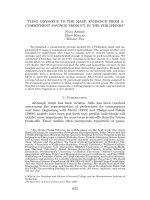
3 Circuit Implementation
Figure 1. System Block Diagram
Figure 1 depicts the system block diagram. The two LEDs are time multiplexed at 500 times per second.
The PIN diode is therefore alternately excited by each LED light source.
The PIN diode signal is amplified by the built in operational amplifiers OA0 and OA1. The ADC12 samples
the output of both amplifiers. The samples are correctly sequenced by the ADC12 hardware and the MCU
software separates the infra-red and the red components.
The SaO
2
level and the heart rate are displayed on an LCD. The real time samples are also sent via an
RS232 to a PC. A separate PC software displays these samples a graphic trace.
Apart from the MCU and four transistors, only passive components are needed for this design.
An off-the-shelf Nellcor-compatible probe 520-1011N is used. This probe has a finger clip integrated with
sensors and is convenient to use. The input to the probe is a D-type 9 pin connector.
2
A Single-Chip Pulsoximeter Design Using the MSP430 SLAA274A–November 2005–Revised June 2010
Copyright © 2005–2010, Texas Instruments Incorporated
MS430FG437
5
10
DAC0
20 Ohm
20 Ohm
5 kOhm
5 kOhm
1 kOhm
1 kOhm
P2.3
Probe
Integrated
LEDs
Infra Red Visible Red
P2.2
www.ti.com
Circuit Implementation
3.1 Generating the LED Pulses
Figure 2. LED Drive Circuit
There are two LEDs, one for the visible red wavelength and another for the infrared wavelength.
In the Nellcor compatible probe, these two LEDs are connected back to back.
To turn them on, an H-Bridge arrangement is used. Figure 2 illustrate this circuit.
Port 2.3 and Port 2.2 drives the complementary circuit. A DAC0 controls the current through the LEDs and
thereby its light output level.
The whole circuit is time multiplexed.
In the MSP430FG437 the internal 12-bit DAC0 can be connected to either pin 5 or pin 10 of the MCU
through software control in the DAC control register. When a pin is not chosen to output the DAC0 signal,
it is set to Hi-Z or low. The base of each transistor has a pulldown resistor to make sure the transistor is
turned off when it is not selected.
3
SLAA274A–November 2005–Revised June 2010 A Single-Chip Pulsoximeter Design Using the MSP430
Copyright © 2005–2010, Texas Instruments Incorporated
Trans−Impedance
Amp
PIN Diode
3pF
OA0
OPA0 Out
5M2
DC + AC
Components
R
30R
OA1
ADC12
DC
Tracking
DAC12_1
LED Level
Control
Extracted DC
Components
Circuit Implementation
www.ti.com
3.2 Sampling and Conditioning the PIN Diode Signal
Figure 3. Input Front End Circuit and LED Control
The photo-diode generates a current from the received light. This current signal is amplified by a
trans-impedance amplifier. OA0, one of the three built in op-amps, is used to amplify this signal. Since the
current signal is very small, it is important for this amplifier to have a low drift current.
The signal coming out of OA0 consists of a large DC component (around 1 V) and a small AC component
(around 10 mV pk-pk).
The large DC component is caused by the lesser oxygen bearing parts of the body tissue and scattered
light. This part of the signal is proportional to the intensity of the light emitted by the LED.
The small AC component is made up of the light modulation by the oxygen bearing parts such as the
arteries plus noise from ambient light at 50/60 Hz. It is this signal that needs to be extracted and amplified.
The LED level control tries to keep the output of OA0 within a preset range using the circuit illustrated in
Figure 2. The Normal Red and Infra Red LEDs are controlled separately to within this preset range.
Effectively, the output from both LEDs matches with each other within a small tolerance.
The extraction and amplification of the AC component of the OA0 output is performed by the second stage
OA1. The DC tracking filter extracts the DC component of the signal and is used as an offset input to
OA1. As OA1 would only amplify the difference it sees between the two terminals, only the AC portion of
the incoming signal is amplified. The DC portion is effectively filtered out.
The offset of OA1 is also amplified and added to the output signal. This needs to be filtered off later on.
4
A Single-Chip Pulsoximeter Design Using the MSP430 SLAA274A–November 2005–Revised June 2010
Copyright © 2005–2010, Texas Instruments Incorporated
TIMER A
CCR0
CCR1
DAC12_1
OA0 Out
OA0 Out
ADC12
TAR
Period = 1 ms
Visible
Red
ON
Visible
Red
ON
Visible
Red
OFF
Infra
Red
ON
Infra
Red
OFF
S/C
S/C
S/C
S/C
S/C
S/C
www.ti.com
Circuit Implementation
3.2.1 Time Multiplexing the Hardware
Figure 4. Time Multiplexing the Hardware
Timer A is used to control the multiplex sequence and automatically start the ADC conversion.
At the CCR0 interrupt, a new LED sequence is initiated with the following:
• The DAC12_0 control bit DAC12OPS is set or cleared depending on which LED is driven. Port 2 is set
to turn on the corresponding LED.
• A new value for DAC12_0 is set to the corresponding light intensity level
• DAC12_1 is set to the DC tracking filter output for that particular LED.
Note that OA1 amplifies the difference between OA0 Out and DAC12_1.
As the intensity of the visible LED is adjusted, the DAC12_1 signal will become a straight line as the OA0
outputs for the two LEDs are equaled.
The ADC conversion is triggered automatically. It takes two samples, one of the OA0 output for DC
tracking and one of the OA1 output, to calculate the heart beat and oxygen level. These two samples are
taken one after the other using the internal sample timer by setting the MSC bit in the ADC control
register.
To conserve power, at the completion of the ADC conversion an interrupt is generated to tell the MCU to
switch off the LED by clearing DAC12_0.
5
SLAA274A–November 2005–Revised June 2010 A Single-Chip Pulsoximeter Design Using the MSP430
Copyright © 2005–2010, Texas Instruments Incorporated
OA1
ADC12
Output = Gain x AC
Component + Small
Offset
DC
Tracking
Filter
Small
Offset
+
−
AC Component
RMS
Calculation
SaO
2
= Fn [RMS(ir)/
RSM(vr)]
Use Infra−Red Samples Only
Heart Rate
Calculation
Input
+
−
K
K = 1/2
9
+
+
Output
Z
−1
Circuit Implementation
www.ti.com
3.3 Signal Conditioning of the AC Components
Figure 5. Signal conditioning of the AC Components
The output of OA1 is sampled by the ADC at 1000 sps. Alternating between the infra-red LED and the
normal-red LED. Therefore each LED signal is sampled at 500 sps.
Samples of the OA1 output must be stripped of the residual dc. A high pass digital filter is impractical
here, as the required cutoff frequency is rather low. Instead a IIR filter is used to track the dc level. The dc
is then subtracted from the input signal to render a final true ac digital signal.
The sampled signal is digitally filtered to remove ambient noise at 50 Hz and above. A low pass FIR filter
with a corner frequency of 6 Hz and -50 dB attenuation at 50 Hz and above is implemented.
At this stage the signal resembles the pulsing of the heart beat through the arteries.
3.3.1 The DC Tracking filters
Figure 6. Tacking Filter Block Diagram
A DC tracking filter is illustrated in Figure 6.
This is an IIR filter. The working of this filter is best understood intuitively. The filter will add a small portion
of the difference between its input and its last output value to its last output value to form the a new output
value. It there is a step change in the input, the output changes itself to be the same as the input over a
period of time. The rate of change is controlled by the coefficient K. K is worked out by experiment.
So if the input contains an AC and DC component, The coefficient K is made sufficiently small to generate
a time constant relative to the frequency of the AC component so that over a length of time the AC will
cancel itself out in the accumulation process and the output would only track the DC component of the
input.
To ensure there is sufficient dynamic range, the calculation is done is double precision, 32 bits. Only the
most significant 16 bits are used.
3.4 Calculating the Oxygen Level and Heart Beat Rate
Because both LEDs are pulsed, traditional analog signal processing has to be abandoned in favor of
digital signal processing.
The signal samples are low pass filtered to remove the 50/60 Hz noise.
For each wavelength of light, the DC value is removed from the signal leaving the AC part of the signal,
which reflects the arterial oxygenation level. The RMS value is calculated by averaging the square of the
signal over a number of heart beat cycles.
6
A Single-Chip Pulsoximeter Design Using the MSP430 SLAA274A–November 2005–Revised June 2010
Copyright © 2005–2010, Texas Instruments Incorporated
RȀ +
log
(
l
ac
)
l1
log
(
l
ac
)
l2
SaO
2
a RȀ
Heart beats per minute +
500 60
ǒ
Samples Count
3
Ǔ
www.ti.com
Circuit Implementation
The DC measurement is continuously calculated by averaging the signals over a number of heart beat
cycles.
The driving strength of each LED is controlled so that the DC level seen at the PIN diode meets a set
target level with a small tolerance. By doing this for each LED, the final results is that the DC levels of
these two LED match one another to within a small tolerance.
Once the DC levels match, then the SaO
2
is calculated by dividing the logs of the RMS values.
(3)
The heart beat is measure by counting the number of samples in 3 beats, since the sampling rate is 500
sps. The heart beat per minute is calculated by:
(4)
Figure 7. Empirical and Theoretical R to SaO
2
Figure 7 shows the difference between the empirical and theoretical R to SaO
2
curve.
As the Oxygen Saturation seldom drops below 80%, a linear relationship with a slight offset can safely be
assumed.
7
SLAA274A–November 2005–Revised June 2010 A Single-Chip Pulsoximeter Design Using the MSP430
Copyright © 2005–2010, Texas Instruments Incorporated
Results
www.ti.com
4 Results
Figure 8. Heart Beat Signal Output
Figure 8 shows the captured Heart Beat signal from the board. This signal is output through the serial port
to the PC at 115 Kbps. An open source application program scope.exe that runs on the PC is also
available with this application notes.
The heart rate/minute is measured and displayed on the LCD.
The Oxygen Saturation percentage is also displayed.
8
A Single-Chip Pulsoximeter Design Using the MSP430 SLAA274A–November 2005–Revised June 2010
Copyright © 2005–2010, Texas Instruments Incorporated
www.ti.com
Parts List
5 Parts List
Table 1. Parts List
QTY VALUE PARTS
2 Tact switch S1, S2
2 1n4148 D4, D5
1 DB9 X2
1 Jumper JP1
1 LCD LCD1
1 Red LED LED3
3 4-pin header SL1, SL2, SL5
1 MAX3221 U2
2 MMBT2222 T1, T2
1 MSP430FG437 U1
1 LED 660nm, Kodenshi BL-23G D2
1 LED 940nm, Kodenshi EL-23G D3
1 Pin-diode, Kodenshi HPI-23G D1
10 0.1uF C1, C5, C6, C7, C8, C12, C13, C14, C15, C19
6 1kΩ R16, R17, R18, R19, R27, R28
3 1uF C3, C9, C20
1 3V battery G1
1 3pF C2
2 4.7nF C16, C17
1 5.1MΩ R3
3 5kΩ R22, R24, R26
(1)
2 10kΩ R13, R14
3 10uF C4, C10, C11
1 15kΩ R9
2 20Ω R1, R2
1 32.768k X1
1 47pF C18
(1)
4 100Ω R4, R5
3 100kΩ R8, R15, R20
1 150kΩ R25
(1)
3 300kΩ R10, R11, R12
1 Buzzer SG2
1 Nellcor compatible probe 520-1011N
(1)
NOTE: If the internal feedback resistor ladder is used for OA1 (as implemented in the application source code), then these parts
do not need to be populated: R25, R26 and C18.
6 References
• Medical Electronics, Dr. Neil Townsend, Michaelmas Term 2001
• MSP430F4xx Family User's Guide (SLAU056)
9
SLAA274A–November 2005–Revised June 2010 A Single-Chip Pulsoximeter Design Using the MSP430
Copyright © 2005–2010, Texas Instruments Incorporated
MSP430FG437PN
+
+
+
LCD1
+
+
+-
+
P1.0/TA0
67
P1.1/TA0/MCLK
66
P1.2/TA1
65
P1.3/TBOUTH/SVSOUT
64
P1.4/TBCLK/SMCLK
63
P1.5/TACLK/ACLK
62
P1.6/CA0
61
P1.7/CA1
60
P2.0/TA2
59
P2.1/TB0
58
P2.2/TB1
57
P2.3/TB2
56
P2.4/UTXD0
55
P2.5/URXD0
54
P2.6/CAOUT/S19
31
P2.7/ADC12CLK/S18
30
P3.0/STE0/S31
43
P3.1/SIMO0/S30
42
P3.2/SOMI0/S29
41
P3.3/UCLK0/S28
40
P3.4/S27
39
P3.5/S26
38
P3.6/S25
37
P3.7/S24/DMAE0
36
P4.0/S9
21
P4.1/S8
20
P4.2/S7
19
P4.3/S6
18
P4.4/S5
17
P4.5/S4
16
P4.6/S3/A15
15
P4.7/S2/A14
14
P5.0/S1/A13
13
P5.1/S0/A12/DAC1
12
P5.2/COM1
45
P5.3/COM2
46
P5.4/COM3
47
P5.5/R13
49
P5.6/R23
50
P5.7/R33
51
P6.0/A0/OA0I0
75
P6.1/A1/OA0O
76
P6.2/A2/OA0I1
77
P6.3/A3/OA1I1/OA1O
2
P6.4/A4/OA1I0
3
P6.5/A5/OA2I1/OA2O
4
P6.6/A6/DAC0/OA2I0
5
P6.7/A7/DAC1/SVSIN
6
AVCC
80
AVSS
78
TCK
73
TMS
72
TDI/TCLK
71
TDO/TDI
70
XIN
8
XOUT
9
XT2IN
69
XT2OUT
68
VEREF+/DAC0
10
VREF+
7
VREF-/VEREF-
11
NMI/RST
74
DVCC1
1
DVSS1
79
DVCC2
52
DVSS2
53
S10
22
S11
23
S12
24
S13
25
S14
26
S15
27
S16
28
S17
29
S20
32
S21
33
S22
34
S23
35
R03
48
COM0
44
U1
T1
T2
R1
R2
R3
R4
R5
R8
R9
R10
R11
R12
C1
C2
3 1
24
S1
3 1
24
S2
X1
1
2
3
4
5
6
7
8
9
10
11
12
13
14
JP1
C1+
2
C1-
4
C2+
5
C2-
6
T1IN
11
R1OUT
9
V+
3
V-
7
T1OUT
13
R1IN
8
INVALID\
10
FORCEOFF\
16
FORCEON
12
EN\
1
U2
1514
GND VCC
U2P
C3
C4
C5
C6C7
C9
R13
R14
R15
C12
C13
C14
C15
R16
R17
R20
COM3
1
COM4
2
COM2
3
COM1
4
S14
5
S13
6
S12
7
S11
8
S10
9
S9
10
S8
11
S7
12
S6
13
S5
14
S4
15
S3
16
S2
17
S1
18
S0
19
COM1_
20
R22
R24
R25
R26
C8
C10 C11
R27
LED3
R28
1
2
3
4
SL1
1
2
3
4
SL2
1
6
2
7
3
8
4
9
5
X2
1
2
3
4
SL5
C18
+-
G1
D4
D5
R18
R19
C19
C20
1
.
1
,
1
`
1
'
1
-
1
"
1
6 2
7 3
8 4
9 5
X3
Q1 Q2
COM3
COM3
COM2
COM2
COM1
COM1
COM0
COM0
S0
S0
S1
S1
S2
S2
S3
S3
S4
S4
S5
S5
S6 S6
S7
S7
S8
S8
S9
S9
S10
S10
S11
S11
S12
S12
S13
S13
S14
S14
5k
20 ohm
5.1M
100 ohm
100 ohm
100k
15k
300k
300k
300k
0.1uF
3pF
32.768k
1uF
10uF
GND
GND
VCC
0.1uF
GND
VCC
0.1uF
0.1uF
1uF
10k
10k
GND
VCC
GND
GND
100k
VCC
VCC
GND
0.1uF
0.1uF
0.1uF
0.1uF
1k
1k
100k
20 ohm
5k
150k
5k
GND
0.1uF
10uF 10uF
1k
1k
GND
GND
VCC
47pF
3V
1k
1k
0.1uF
1uF
Nellcor compatible 520-1011N
BC856ASMD BC856ASMD
Schematic
www.ti.com
7 Schematic
10
A Single-Chip Pulsoximeter Design Using the MSP430 SLAA274A–November 2005–Revised June 2010
Copyright © 2005–2010, Texas Instruments Incorporated
IMPORTANT NOTICE
Texas Instruments Incorporated and its subsidiaries (TI) reserve the right to make corrections, modifications, enhancements, improvements,
and other changes to its products and services at any time and to discontinue any product or service without notice. Customers should
obtain the latest relevant information before placing orders and should verify that such information is current and complete. All products are
sold subject to TI’s terms and conditions of sale supplied at the time of order acknowledgment.
TI warrants performance of its hardware products to the specifications applicable at the time of sale in accordance with TI’s standard
warranty. Testing and other quality control techniques are used to the extent TI deems necessary to support this warranty. Except where
mandated by government requirements, testing of all parameters of each product is not necessarily performed.
TI assumes no liability for applications assistance or customer product design. Customers are responsible for their products and
applications using TI components. To minimize the risks associated with customer products and applications, customers should provide
adequate design and operating safeguards.
TI does not warrant or represent that any license, either express or implied, is granted under any TI patent right, copyright, mask work right,
or other TI intellectual property right relating to any combination, machine, or process in which TI products or services are used. Information
published by TI regarding third-party products or services does not constitute a license from TI to use such products or services or a
warranty or endorsement thereof. Use of such information may require a license from a third party under the patents or other intellectual
property of the third party, or a license from TI under the patents or other intellectual property of TI.
Reproduction of TI information in TI data books or data sheets is permissible only if reproduction is without alteration and is accompanied
by all associated warranties, conditions, limitations, and notices. Reproduction of this information with alteration is an unfair and deceptive
business practice. TI is not responsible or liable for such altered documentation. Information of third parties may be subject to additional
restrictions.
Resale of TI products or services with statements different from or beyond the parameters stated by TI for that product or service voids all
express and any implied warranties for the associated TI product or service and is an unfair and deceptive business practice. TI is not
responsible or liable for any such statements.
TI products are not authorized for use in safety-critical applications (such as life support) where a failure of the TI product would reasonably
be expected to cause severe personal injury or death, unless officers of the parties have executed an agreement specifically governing
such use. Buyers represent that they have all necessary expertise in the safety and regulatory ramifications of their applications, and
acknowledge and agree that they are solely responsible for all legal, regulatory and safety-related requirements concerning their products
and any use of TI products in such safety-critical applications, notwithstanding any applications-related information or support that may be
provided by TI. Further, Buyers must fully indemnify TI and its representatives against any damages arising out of the use of TI products in
such safety-critical applications.
TI products are neither designed nor intended for use in military/aerospace applications or environments unless the TI products are
specifically designated by TI as military-grade or "enhanced plastic." Only products designated by TI as military-grade meet military
specifications. Buyers acknowledge and agree that any such use of TI products which TI has not designated as military-grade is solely at
the Buyer's risk, and that they are solely responsible for compliance with all legal and regulatory requirements in connection with such use.
TI products are neither designed nor intended for use in automotive applications or environments unless the specific TI products are
designated by TI as compliant with ISO/TS 16949 requirements. Buyers acknowledge and agree that, if they use any non-designated
products in automotive applications, TI will not be responsible for any failure to meet such requirements.
Following are URLs where you can obtain information on other Texas Instruments products and application solutions:
Products Applications
Amplifiers amplifier.ti.com Audio www.ti.com/audio
Data Converters dataconverter.ti.com Automotive www.ti.com/automotive
DLP® Products www.dlp.com Communications and www.ti.com/communications
Telecom
DSP dsp.ti.com Computers and www.ti.com/computers
Peripherals
Clocks and Timers www.ti.com/clocks Consumer Electronics www.ti.com/consumer-apps
Interface interface.ti.com Energy www.ti.com/energy
Logic logic.ti.com Industrial www.ti.com/industrial
Power Mgmt power.ti.com Medical www.ti.com/medical
Microcontrollers microcontroller.ti.com Security www.ti.com/security
RFID www.ti-rfid.com Space, Avionics & www.ti.com/space-avionics-defense
Defense
RF/IF and ZigBee® Solutions www.ti.com/lprf Video and Imaging www.ti.com/video
Wireless www.ti.com/wireless-apps
Mailing Address: Texas Instruments, Post Office Box 655303, Dallas, Texas 75265
Copyright © 2010, Texas Instruments Incorporated