Engineering Materials and Processes phần 2 pptx
Bạn đang xem bản rút gọn của tài liệu. Xem và tải ngay bản đầy đủ của tài liệu tại đây (254.46 KB, 14 trang )
Introduction 5
1.2 Properties of Silver, Copper and Aluminum
A comparison of the electrical, physical, mechanical, and thermal properties of
silver, copper, and aluminum is given in Table 1.1.
Table 1.1. Comparison of properties of Ag with Cu and Al
Properties Ag Cu Al
Bulk resistivity
(μΩ-cm) at 20 °C
1.59
1.68
2.65
Thin film resistivity
(μΩ-cm) at 20 °C
2.0 (Ag/Ti)
2.0–2.5 (Cu/Cr)
2.8 (Cu/Ni)
3.3 (Al-Cu)
Diffusivity in Si
(cm
2
/sec)
2.3×10
–3
e
–1.6/kT
4.2×10
–2
e
–1.0/kT
–
Self-diffusivity
(cm
2
/sec)
0.67e
–1.97/kT
0.78 e
–2.19/kT
1.71 e
–1.48/kT
Electromigration
activation energy
(eV)
0.95
(225–285 °C)
1.1
(250–395 °C)
0.4–0.8
Young’s modulus
(×10
11
dyn cm
–2
)
8.27
12.98
7.06
TCR×10
3
(K
–1
)
4.1
4.3
4.0
Mean free path of e
–
(nm)
52.0
39.0
15.0
Melting point (°C)
961
1083
917
Thermal
conductivity
(Wcm
–1
K
–1
)
4.25
3.98
2.38
6 Silver Metallization
1.3 References
[1] J. M. E. Harper, K. L. Holloway, T. Y. Kwok, US Patent No. 5,130,274
(1992).
[2] The National Technology Roadmap for Semiconductors, Semiconductor
Industry Association, San Jose, CA, 1994.
[3] J. Li, J. W. Mayer, Y. Shacham-Diamand, E. G. Colgan, Appl. Phys. Lett.
60. 2983(1992).
[4] D. Adams, and T. L. Alford, Materials Science and Engineering: Reports
40, 207(2003).
[5] T. Iijima, H. Ono, N. Ninomiya, Y. Ushiku, T. Hatanaka, A. Nishiyama,
H. Iwai, Extended Abstracts of the 1993 International Conference on Solid
State Devices and Materials, Makuhari, 183(1993).
[6] S. P. Murarka, R. J. Guttman, A. E. Kaloyeros, W. A. Lanford, Thin Solid
Films 236, 257(1993).
[7] J. D. McBrayer, R. M. Swanson, T. W. Sigmon, J. Electrochem. Soc. 133
1243(1986).
[8] T. E. Graedel, J. Electrochem. Soc. 139(7), 1963(1992).
[9] B. Chalmers, R. King, R. Shuttleworth, Proc. R. Soc. A 193, 465(1948).
[10] A. E. B. Presland, G. L. Price, D. L. Trimm, Prog. Surf. Sci. 3, 63(1973).
[11] S. K. Sharma, J. Spitz, Thin Solid Films 65, 339(1980).
[12] K. Sharma, J. Spitz, Thin Solid Films 66, 51(1980).
[13] P. N. Nguyen, Ph.D. thesis, Arizona State University, 2000.
[14] P. N. Nguyen, Y. Zeng, T. L. Alford, J. Vac. Sci. Technol. B 17(5),
2204(1999).
[15] T. L. Alford, P. N. Nguyen, Y. Zeng, J. W. Mayer, Microelectronics
Engineering 55, 383(2001).
2
Silver Thin Film Characterization
2.1 Introduction
Thin films of Ag layered structures, typically less than a micron in thickness, are
tailored to achieve desired functional properties. Typical characterization is the
instrumentations that use X-ray and ion beams to probe the properties of the film.
This work discusses two techniques in thin film analysis, Rutherford
backscattering spectrometry (RBS) [1, 2] and X-ray diffractrometry (XRD) [3, 4]
which emphasize composition and lattice measurements, respectively.
Advancement in RBS and X-ray analyses are developed in response to the needs of the
microelectronics and forensic disciplines.
Analysis of metallization on SiO
2
is typically done with Rutherford
backscattering at 2.0 MeV energies and with semiconductor nuclear particle
detectors. The resonance analysis of these species is done in the same experimental
chamber as used in RBS, but the energy of the incident helium ions is increased to
energies where there are resonances in the backscattering cross sections [5, 6]. These
resonances increase the yield of the scattered particle by nearly two orders of
magnitude and provide high sensitivity to the analysis of oxygen and carbon in
silicon. The use of these high energies, 3.05 and 3.7 MeV for the helium-oxygen
and helium-nitrogen resonances respectively is called resonance scattering or non-
Rutherford scattering.
In a similar manner XRD is also considered as a nondestructive characterization
technique. XRD is used to monitor the phases and structure present in the film. Also
the lattice parameter, strain and texturing can be resolved using pole figure analysis
[3, 4].
8 Silver Metallization
2.2 Rutherford Backscattering Spectrometry
In a typical scattering chamber, the sample is located such that the beam position
does not shift across the sample as the sample is tilted with respect to the
incident ion beam. The backscattering detector is mounted as close to the
incident beam as possible such that the average backscattering angle, ϑ, is
close to 180°, typically 170°, with a detector solid angle of 5 millisteradians
(msr). The vacuum requirements in the target chamber are comparable to those in
the accelerator beam lines. Enhanced vacuum levels reduce the probability that the
ion beam will lose energy along its path to the sample and also minimizes deposition
of contaminants and hydrocarbons on the surface during analysis.
In traditional backscattering spectrometry using helium ions, the energy
resolution of the solid-state particle detector is typically >17 keV. The output
signal, which is typically millivolts in pulse height is processed by silicon
integrated circuit electronics and provides an energy spectrum in terms of
number of particles versus energy. A multichannel analyzer records the
number of backscattered particles versus a given energy in a specific channel.
2.2.1 Scattering Kinematics
During ion-beam analysis the incident particle penetrates into the target and undergoes
inelastic collisions with the electrons in the samples and loses energy as it
penetrates. During the penetration of the helium ions a small fraction undergo
elastic collisions with the target atom, which defines the backscattering signal.
Figure 2.1 shows a schematic representation of the geometry of an elastic collision
between a projectile of mass M
1
and energy E
o
with a target atom of mass M
2
initially at rest. After collision the incident ion is scattered back through an angle ϑ
and emerges from the sample with an energy E
1
. The target atom after collision
has a recoil energy E
2
. There is no change in target mass, because nuclear reactions
are not involved and energies are non-relativistic. The ratio of the projectile
energies for M
1
< M
2
is given by:
2
1
222
2
121 1
o21
E(MMsin)Mcos
K
EMM
⎡⎤
−ϑ+ϑ
⎢⎥
==
⎢⎥
+
⎢⎥
⎣⎦
(2.1)
The energy ratio K = E
1
/E
o
, called the kinematic factor, shows how the energy
of the backscattered particle is a function of the incident particle and target atoms
masses, the scattering angle, and incident energy.
The ability to identify different mass species depends on the energy resolution
of the detector which is typically 17 keV full width at half maximum (FWHM).
For example, Ag has a mass M
2
= 108 and In has a mass M
2
= 115. The difference
between K
Ag
= 0.862 and K
In
= 0.870 is 0.008. For 2.8 MeV helium ions, the
difference in backscattering energy is 22 keV which is larger than the detector-
system resolution, indicating that signals from Ag and In on the surface can be
resolved.
Silver Thin Film Characterization 9
Figure 2.1. A schematic representation of an elastic collision between a particle of mass M
1
and initial energy E
0
and a target atom of mass M
2
. After the collision the projectile and
target atoms have energies of E
1
and E
2
, respectively.
2.2.2 Scattering Cross Section
The identity of target elements is established by the energy of the scattered
particles after an elastic collision. This is done by measuring the yield Y, the
number of backscattered particles for a given value of incident particles Q.
The detector’s solid angle is given as Ω. The areal density, the number of
atoms per unit area, N
S
is determined from the scattering cross section σ (ϑ) by:
()
=
σϑ Ω
s
Y
N
Qd
(2.2)
For a narrow beam of fast particles impinging upon a thin uniform target that is
wider than the beam and at an tilt angle ϑ, the simplest approximation for the
scattering cross section is given by:
()
2
2
12
4
ZZe
1
.
4E
sin
2
⎛⎞
σϑ=
⎜⎟
ϑ
⎝⎠
(2.3)
which is the scattering cross section originally derived by Rutherford. For 2 MeV
helium ions incident on silver, Z
2
= 47 at an angle of 180º, the cross section is
2.9×10
–24
cm
2
or 2.9 barns (where the barn = 10
–24
cm
2
). The distance of closest
θ
φ
Projectile, M
1
E
0
Target, M
2
Detector
E
1
M
1
E
2
φ
10 Silver Metallization
approach is about 7×10
–3
nm which is smaller than the K-shell radius of silver
(10
–1
nm).
2.2.3 Depth Scale
Light ions such as helium lose energy through inelastic collision with atomic
electrons. In backscattering spectrometry, where the elastic collision takes place at
depth t below the surface, one considers the energy loss along the inward path and
on the outward path as shown in Figure 2.2. The energy loss on the way in is
weighted by the kinematic factor and the total is given by the relationship:
[]
1
.
cos
⎛⎞
Δ=Δ + =Δ
⎜⎟
⎜⎟
ϑ
⎝⎠
in out
dE dE
EtK tS
dx dx
(2.4)
where dE/dx is the rate of energy loss with distance and [S] is the energy loss
factor. The particle loses energy ΔE
in
via inelastic collisions with electrons along
the inward path. There is energy loss ΔE
s
in the elastic scattering process at depth
t. There is energy loss due to inelastic collisions ΔE
out
along the outward path.
Figure 2.2. Energy loss components for a projectile that scatters from depth t. The particle
loses energy ΔE
in
via inelastic collisions with electrons along the inward path. There is
energy loss ΔE
s
in the elastic scattering process at depth t. There is energy lost to inelastic
collisions ΔE
out
along the outward path.
E
0
E
1
ΔE
i
ΔE
out
De
p
th t
Depth
10 20 30
ΔE
s
in
Silver Thin Film Characterization 11
An example illustrating the influence of depth on analysis is given in Figure
2.3, which shows two thin silver layers on the front and back of a titanium film.
The scattering from silver at the surface is clearly separated from Ag at the back
layer. The energy width between the Ag signals is closely equal to that of the
energy width of the Ti signal. The depth scales are determined from energy loss
values.
Figure 2.3. Backscattering spectrum of a Ti film (150 nm) with thin layers of Ag (3 nm) on
the front and back surfaces of the titanium
2.2.4 Ion Resonances
At energies of a few MeV nuclear reactions and strong deviations from Rutherford
scattering can result in a strong increase (resonance) in the scattering cross section
(for example at 3.04 MeV for
4
He ions incident on
16
O). This reaction can be used
to increase the sensitivity for the detection of oxygen as well as other light
elements such as carbon and nitrogen. In order to evaluate the amount of oxygen in
Ag diffusion barriers (e.g., TiAl
x
N
y
O
z
) on SiO
2
/Si substrate, the oxygen resonance
technique using 3.05 MeV
4
He
+2
ion beam was employed (Figure 2.4). The RUMP
simulation [7] overlaps the collected spectrum. The enhanced oxygen peak near
channel 200 is a direct consequence of O resonance at 3.05 MeV and corresponds
to oxygen atoms present in the thin film.
12 Silver Metallization
Figure 2.4. RBS spectrum (3.05 MeV He
+2
, 7° tilt) and simulation of as-deposited
TiAl
x
N
y
O
z
thin film on SiO
2
/Si substrate
2.3 X-ray Diffractometry
W. L. Bragg derived a description of coherent scattering from an array of periodic
scattering sites, i.e., atoms in a crystalline solid. The scalar description of
diffraction considers the case of monochromatic radiation impinging on two sheets
of atoms in the crystal spaced d
hkl
between reflecting planes. The wavelength λ of
the radiation is smaller than the interatomic spacing d
hkl
of the specific (hkl) planes.
Bragg invoked the Law of Reflectivity (or Reflections) that states that the
scattering incident angle and exiting angle must be equal, ϑ
in
= ϑ
out
under the
condition of coherent scattering. The wavelets scattered by the atoms combine to
produce constructive interference if the total path difference 2*ΔP for the reflected
waves equals integer (n) multiples of λ:
nλ = 2ΔP = 2d
hkl
sinϑ (2.5)
Hence, Bragg’s Law: nλ = 2d
hkl
sinϑ defines the condition for diffraction. The
simplest of all modern X-ray analyses is powder analysis using an X-ray
diffractometer. The technique can be used to characterize polycrystalline thin films
Silver Thin Film Characterization 13
as well. The sample under investigation is placed on the sample stage of the
diffractometer. The key components of a typical diffractometer include a sample
stage, monochromatic radiation source, and radiation electronic solid-state
detection system. The scattered X-rays dissipate energy by generation of electron-
hole pairs in the detector. The electronic system converts the collected charge into
voltage pulses which are directly proportional to the intensity of the diffracted X-
ray beam. The typical X-ray spectrum is a plot of intensity verses angle, e.g., 2ϑ.
The phase can be indentified by comparing the spectrum to Joint Committee on
Powder Diffraction Standards (JCPDS) cards. Figure 2.5 shows an typically XRD
spectrum from a 200 nm thick, polycrystalline Ag layer on a single crystalline Si
substrate.
Figure 2.5. XRD spectrum of a 200 nm polycrystalline Ag layer on a single crystalline Si
substrate. The indexed peaks correspond to specific reflections. The forbidden Si(002)
reflection is due the double difraction of the strong (004) reflection.
2.4 References
[1] W. K. Chu, J. W. Mayer, and M. A. Nicolet, Backscattering Spectrometry,
Academic Press, New York, 1978.
[2] J. W. Mayer, E. Rimini, Ion Handbook for Material Analysis, Academic
Press, New York, 1977.
[3] B. D. Cullity and S. R. Stock, Elements of X-ray Diffraction, Prentice Hall,
NJ, 2001.
[4] T. L. Alford, Feldman, L. C.; J. W. Mayer, Fundamentals of Nanoscale
Analysis, Springer, New York, 2007.
(d)
Ag (222)
Ag
(311)
Ag (111)
Si (004)
Ag (200)
Si
(002)
a
.u.)
30 40 50 60 70 80 90
2
θ
(degree)
Relative Intensity
14 Silver Metallization
[5] S. W. De Coster, B. Brijs, J. Goemans, and W. Vandervost, Nucl. Instr.
Meth. B 66, 128318(1992).
[6] S. W. Russell, T. E. Levine, A. E. Bair, and T. L. Alford, Nucl. Instr.
Meth. B 118, 118(1996).
[7] L. R. Doolittle, Nucl. Instr. Meth. B 15, 227(1986).
3
Diffusion Barriers and Self-encapsulation
3.1 Introduction
As feature sizes in multilevel metallization continue to shrink, the thermal stability
of metallization and barrier layers become more critical for device reliability. The
application of silver in multilevel metallization schemes require thermal stability
when in contact with other metal layers and dielectrics. Therefore, developing a
suitable diffusion barrier to retard the diffusion of Ag into adjacent materials and to
prevent agglomeration is indispensable for the Ag metallization scheme. There
have been extensive efforts to investigate qualified diffusion barrier layers
interposed between Ag and SiO
2
[1]. The stability of silver thin films on various
underlying layers at elevated temperatures has also been investigated [1]. Several
authors have investigated the behavior of Ag on SiO
2
/Si substrates [2, 3]. The
addition of a thin Au layer between the Ag and Si was found to improve the
stability of the interface by forming an intermixed region, resulting in a lowering of
the interfacial energy of the Ag/Si system [3].
Refractory metal nitrides such as TiN, TaN, and WN are widely recognized as
attractive materials for use as diffusion barriers in metal-semiconductor contacts
due to their high stability and good conductivity [4]. TaN has been studied as a
diffusion barrier for copper metallization since it is thermodynamically stable with
Cu and due to the absence of any compound formation between Cu and Ta, and
between Cu and N [5].
Diffusion barriers are used to prevent degradation of devices as a result of poor
adhesion and interdiffusion. The objective is to find an intermediate layer between
the interconnect Ag metal and the underlying dielectric that will act as both an
16 Silver Metallization
adhesion promoter and an effective diffusion barrier between interconnect metal
and adjacent materials.
3.2 Titanium-Nitride Self-encapsulation of Silver Films
3.2.1 Introduction
The existing metallization schemes for ohmic contacts, gate metal and
interconnections are found to be inadequate for the development of ultra large scale
integration (ULSI) and gigascale integration (GSI). These inadequacies include the
reliability of aluminum and its alloys as current carriers, susceptibility to
electromigration and the relatively high resistivity of Al (~2.7 µΩ-cm). For the
development of faster devices, the resistance-capacitance (RC) delay must be
reduced. Advanced metallization schemes using so-called multilevel metallization
(MLM) structures of a low resistivity metal such as Cu have been proposed to
reduce the resistance component of the RC delays [6].
Currently copper and silver, noted for low resistivities and higher resistance to
electromigration, are being investigated as future interconnect materials [7, 8].
Despite this they have not found extensive application in ICs because of their (a)
high diffusivity and deep levels in silicon, (b) poor adhesion to SiO
2
and
polyimide, and (c) reactivity with the environment. To make copper and silver
metallization manufacturable, adhesion promoters, protection against corrosive
environments and the development of a process to define interconnection wiring
will be needed.
The three most commonly used techniques to enhance the adhesion between the
dielectric and silver are: (i) the use of adhesion promoters; (ii) increased
temperature of deposition or providing energy to ionize depositing species; (iii)
surface pretreatment, especially plasma oxidation of polymers, sputter damage of
metal surfaces or use of ion implantation near the polymer or metal surface. The
use of adhesion promoters seems attractive since they can also act as diffusion
barriers at higher process temperatures. Titanium, TiW and TiN have been most
frequently used because of titanium’s excellent chemical reactivity with oxygen,
carbon, nitrogen, and fluorine.
Diffusion Barriers and Self-encapsulation 17
3.2.2 Experimental Details
Alloy films consisting of ~200 nm Cu (27 at.% Ti), and Ag(6–26 at.% Ti) were co-
deposited by electron-beam evaporation onto thermally grown SiO
2
(100–200 nm)
on (100) Si substrates. The stoichiometry and thicknesses of all the as-deposited
samples were determined by Rutherford backscattering spectrometry (RBS).
Samples were annealed for 10–120 minutes at temperatures ranging from 300 to
700°C in a Lindberg single-zone quartz-tube furnace in a flowing electronic grade
(99.99%, with H
2
O < 33 and O
2
+ Ar < 10 molar ppm) ammonia (NH
3
) ambient at
atmospheric pressure, to form the refractory metal nitrides. Before each anneal the
annealing chamber was evacuated to about 10 mTorr followed by a 2.5 minute
purge with NH
3
. This sequence was repeated twice with a final 20 minute purge.
To minimize the chances of oxidation, flow rates of ~2–8 l/min were maintained
during the annealing. Free surface as well as interfacial reactions was analyzed by
RBS and Auger electron spectroscopy (AES). The RBS analysis was performed
using 1.7 MV Tandem Accelerator with He
+2
beam energies between 2.0 and 4.3
MeV. The backscattering angle was 170° and the total accumulated charge was
10–20 µC. The samples were tilted at 7°. We utilized the computer simulation
program RUMP for simulation and interpretation of RBS spectra.
After annealing, the sheet resistance of certain samples was measured by the
four-point-probe method. The resistivity was determined from the sheet resistance
and thickness of dealloyed Cu or Ag film only. Here, the measured resistivity was
considered to be that of the metal layers. The contribution of the surface Ti-
oxynitride layer resistivity to the total resistivity was less than 1%, because the
ratio of the nitride thickness to Ag or Cu thickness was approximately 1:10.
3.2.3 Results
All anneals in this section were performed for 30 minutes in a flowing NH
3
ambient. Figure 3.1 compares the RBS spectrum of the as-deposited Ag(19 at.%
Ti) alloy with that nitrided at 450°C and 600°C. After a 450°C anneal, the presence
of a “Surface Ti” peak and a distinct “Interfacial Ti” peak indicates that Ti
segregated to the free surface and also reacted with the SiO
2
substrate.
18 Silver Metallization
Figure 3.1. RBS spectra showing the depth distributions of Ag and Ti of a 210 nm-thick
Ag(19 at.% Ti) alloy, before and after annealing at 450°C and 600°C for 30 minutes in NH
3
.
A 2.0 MeV He
+2
beam energy was used [9].
The surface and interfacial reactions result in the formation of a TiN(O) layer
and Ti-oxide/Ti-silicide bilayer structure, respectively. Computer RUMP
simulation of the spectrum corresponding to the 450°C anneal, suggests that the
dealloyed Ag layer contains a residual Ti concentration of ~10.8 at.%. The TiN(O)
thickness is ~17 nm. Anneals at 600°C result in a more dealloyed Ag layer, with a
residual Ti concentration as low as 0.9 at.%.
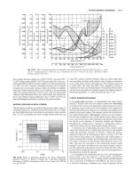
Figure 3.2 shows the residual Ti concentration as a function of annealing time
for an Ag(26 at.% Ti) alloy. For all temperatures rapid dealloying occurs within the
first 10 minutes; thereafter little or no further outdiffusion of Ti takes place. On the
other hand, strong temperature dependence is evident. Ag(Ti) alloys with initial Ti
concentrations of 6, 10 and 19 at.% showed similar dealloying behavior.