Digital logic testing and simulation phần 6 pdf
Bạn đang xem bản rút gọn của tài liệu. Xem và tải ngay bản đầy đủ của tài liệu tại đây (547.52 KB, 70 trang )
A TESTBENCH
327
In this chapter, fault simulation and ATPG will be examined from the user’s per-
spective. What kind of reports should be generated, and how do test programs get
translated into tester format? Users have, in the past, been quite critical of fault sim-
ulators, complaining that they simply produced a fault coverage number based on
the test vectors and the fault list, without producing any meaningful suggestions,
help, or insight into how to improve on that number. We will examine ways in which
fault simulation results can be made more meaningful to the end user.
The workflow depicted in Figure 7.2 is quite general; it could describe almost any
design project. The circuit being designed may be constrained by rigid design rules
or it may be free form, with the logic designers permitted complete freedom in how
they go about implementing their design. However, as details get more specific (e.g.,
is the design synchronous or asynchronous?), choices start becoming bounded. Many
of the vexing problems related to testing complex sequential circuits will be post-
poned to subsequent chapters where we address the issue of design-for-testability
(DFT). For now, the focus will be on the fault simulator and the ATPG and how their
interactions can be leveraged to produce a test program that is thorough while at the
same time brief.
7.4 A TESTBENCH
A testbench will be created for the circuit in Figure 7.3 using Verilog. A VHDL
description at the structural level would be quite similar, and the reader who under-
stands the following discussion should have no difficulty understanding an equiva-
lent VHDL description of this circuit. The testbench instantiates two modules; the
first is the circuit description, while the second contains the test stimuli, including
timing data. The circuit description is hierarchical, containing modules for a mux
and a flip-flop. The test stimulus module follows the hierarchical netlist testbench.
7.4.1 The Circuit Description
The Verilog circuit description that follows is rather brief. The reader who wishes to
acquire a more thorough understanding of the Verilog HDL is encouraged to consult
Figure 7.3
Gate-level interconnection.
SEL
CLR
E
CK
TSE
C
D
Y
Clr
F
G
B
A
328
DEVELOPING A TEST STRATEGY
one of the many textbooks dedicated to that subject. Because the language is quite
robust, the following code represents but one of several ways to describe a particular
behavior. Also note that the first line of each module is set in boldface for conve-
nience in locating the start of each new module.
'timescale 1 ns / 100 ps
module testbench;
ckt7p3 X1 (tse, sel, ck, clr, y);
stimuli X2 (tse, sel, ck, clr, y);
endmodule
module ckt7p3 (tse, sel, ck, clr, y);
input tse, sel, ck, clr;
inout y;
wire hold;
wire load, choose;
mux2 x1 (.A(hold), .B(load), .Sel(sel), .C(choose));
dff x2 (.Q(hold),.QN(),.data(choose),.clock(ck),
.preset(1'b1),.clear(clr));
bufif1 #(7,7) x3 (y, hold, tse);
buf #(4,4) (load, y);
endmodule
module mux2(A, B, Sel, C);
input A, B, Sel;
output C;
not #(5,5) n1 (Sel_, Sel);
and #(5,5) n2 (L1, Sel_, A);
and #(5,5) n3 (L2, Sel, B);
or #(6,6) n4 (C, L1, L2);
endmodule
module dff(Q,QN,data,clock,preset,clear);
input data; input clock; input preset; input clear;
output Q;
output QN;
nand #(5,5)N1 (L1, preset,L4, L2),
N2 (L2, L1, clear, clock),
N3 (L3, L2, clock, L4), N4 (L4, L3, data, clear),
N5 (Q, preset, L2, QN), N6 (QN, Q, L3, clear);
endmodule
module stimuli(tse, sel, ck, clr, y);
output tse, sel, ck, clr;
inout y;
A TESTBENCH
329
reg [3:0] inputs;
reg ck;
parameter clock_high = 50; // 100ns period, clock high 50ns
'define cycle #1000 inputs = 4'b
assign {tse, sel, clr, y} = inputs;
initial begin
ck = 0;
$dumpfile("ckt7p3.dump");
$dumpvars(3, X1);
$monitor($time,," tse = %b sel = %b ck = %b clr = %b
y = %b",
tse, sel, ck, clr, y);
'include "ckt7p3.fvc" // include vector file
$finish; // end simulation
end
always #clock_high ck = ~ck;
endmodule
// ckt7p3.fvc tse, sel, clr, y
#0 inputs = 4'b110Z; // Reset
'cycle 0111; 'cycle 0111;
'cycle 101Z; 'cycle 101Z;
'cycle 110Z; 'cycle 111Z;
'cycle 0111; 'cycle 101Z;
'cycle 101Z; 'cycle 0110;
The first module in the listing is the top-level testbench, aptly named
testbench
. It
begins with a timescale compiler directive that allows modules with different time
units to be simulated together. The first number specifies the unit of measurement
for delays in the module, and the second number specifies the accuracy with which
delay values are rounded before being used in simulation. In the modules that fol-
low, delays are multiples of 1 ns, and they are rounded to 100 ps during simulation.
So, if a delay value of 2.75 is specified, it represents 2.75 ns and is rounded to 2.8 ns.
The next entry is the name of the module, which ends with a semicolon, as do most
lines in Verilog. The modules
ckt7p3
and
stimuli
are then instantiated.
Ckt7p3
con-
tains the circuit description while the module
stimuli
contains the test program. End-
module is a keyword denoting the end of the module.
The circuit
ckt7p3
again begins by listing the module name, followed by a declara-
tion of the I/O ports in the circuit. The second line of ckt7p3 defines the ports
tse
,
sel
,
ck
, and
clr
as inputs. The third line defines the port
y
as an inout—that is, a bidirec-
tional signal. The signals
hold
,
load
, and
choose
are internal signals. As wires, they
can carry signals but have no persistence; that is, there is no assurance that values on
those signals will be valid the next time the module is entered during simulation.
330
DEVELOPING A TEST STRATEGY
The next line instantiates
mux2
. It is a two-input multiplexer whose definition fol-
lows the definition for
ckt7p3
. Note that the signals in
mux2
are associated with
wires in
ckt7p3
by using a period (.) followed by the signal name from
mux2
and
then the wire called
hold
in
ckt7p3
is enclosed in parentheses. The signal named
Q
in
dff
is also associated with the wire
hold
. It is not necessary to associate names in
this fashion, but it is less error-prone. If this method is not employed, then signals
become position-dependent; in large circuits, errors caused by signals inadvertently
juxtaposed can be extremely difficult to identify.
The
dff
instantiated in
ckt7p3
is the next module listed. It corresponds to the cir-
cuit in Figure 2.8. The signal 1’b1 connected to the preset in the
dff
denotes a logic
1. Similarly, 1’b0 denotes a logic 0. The next element in
ckt7p3
is called
bufif1
. The
bufif1
is a tri-state buffer and is a Verilog primitive. There is a corresponding ele-
ment called
bufif0
.
Bufif1
is active when a logic 1 is present on its enable pin. Bufif0
is active when the enable signal is a logic 0. Other Verilog primitives in the above
listing include buf, and, or, and nand. Any Verilog simulator must provide simula-
tion capability for the standard primitives.
Verilog does not support built-in sequential primitives for the latches and flip-
flops; however, it does support user-defined primitives (UDPs). The UDP is defined
by means of a truth table, and the facility for defining UDPs allows the user to
extend the set of basic primitives supported by Verilog. Through the use of UDPs it
is possible for the user to define any combination of gates as a primitive, so long as
the model only contains a single output pin. Sequential elements can also be defined.
The requirement is that the sequential element must directly drive the output.
7.4.2 The Test Stimulus Description
The module called stimuli has the same I/O ports as ckt7p3. However, in this module
the signals that were inputs in ckt7p3 have become outputs. The inout signal y
remains an inout. A 4-bit register named inputs is defined. The “reg” denotes an
abstract storage element that is used to propagate values to a part. The signal called
ck is defined as a register. Then a parameter called clock_high is defined and set
equal to 500. That is followed by the definition of the ASCII string #1000
inputs = 4’b. These two statements are used to define a clock period of 1000 ns, with
a 50% duty cycle. The values in the register inputs are assigned to the input and
inout signals by means of the assign statement that follows.
An initial statement appears after the assign statement. The first initialization
statement causes a 0 to be assigned to ck prior to the start of simulation. Then a
dump-file statement appears; it causes internal signal values to be written to a dump
file during simulation. The dumpvars statement requests that the dump be per-
formed through three levels of hierarchy. The dump file holds values generated by
internal signals during simulation so that they can later be retrieved for visual wave-
form display.
In the ckt7p3 circuit, there are three levels of hierarchy; the top level contains
mux2 and dff, and these in turn contain lower-level primitive elements. The monitor
statement requests that the simulator print out specified values during simulation so
FAULT MODELING
331
that the user can determine whether the simulation was successful. It instructs the
simulator on how to format the signal values. The text enclosed in quotes is the for-
mat statement; it is followed by a list of variables to be printed. The include state-
ment requests that a file named ckt7p3.fvc be included; this file contains the stimuli
to be simulated. The $finish indicates the end of simulation. The ck signal is
assigned an initial value of 0. Then, every 500 ns it switches to the opposite state.
The next file contains the stimuli used during simulation. Although the stimuli in
this example are vectors listed in matrix form, they could just as easily be generated
by a Verilog model whose sole purpose is to emit stimuli at random times, thus imi-
tating the behavior of a backplane. In this vector file, the word cycle is replaced by
the ASCII text string defined in stimuli.v. That text contains a time stamp, set to the
value 1000. The simulator applies each vector 1000 time units after the previous
vector. The time stamp is followed by the variable inputs; it causes the following
four values to be assigned to the variable inputs from which they will subsequently
be assigned to the four I/O ports by the assign statement.
The values begin with the number 4, indicating the number of signal values in the
string; the apostrophe and the letter b indicate that the string is to be interpreted as a
set of binary signals. The four values follow, ended by a semicolon. The values are
from the set {0, 1, X, Z}. The fourth value is applied to the inout signal y. Recall the
y is an inout; sometimes it acts as an input, and other times it acts as an output.
When y acts as an input, a logic 0 or 1 can be applied to that pin. When y acts as an
output, then the I/O pad is being driven by the tri-state buffer, so the external signal
must be a floating value; in effect the external driving signal is disconnected from
the I/O pad.
7.5 FAULT MODELING
In Chapter 3 we introduced the basic concept of a stuck fault. That was followed by
a discussion of equivalence and dominance. The purpose of equivalence and domi-
nance was to identify stuck-at faults that could be eliminated from the fault list, in
order to speed up fault simulation and test pattern generation, without jeopardizing
the validity of the fault coverage estimate computed from the representative faults.
Other factors that must be considered were postponed so that we could concentrate
on the algorithms. The fault list is determined, at least in part, by the primitives
appearing in the netlist. But, even within primitives, defects in different technologies
do not always produce similar behavior, and there are several MOS and bipolar tech-
nologies in use.
7.5.1 Checkpoint Faults
Theorem 3.3 asserted that in a fanout-free circuit realized by symmetric, unate gates,
it was sufficient to put SA1 and SA0 faults on each primary input. All of the interior
faults are either equivalent to or dominate the faults on the primary inputs. All faults
interior to the circuit will be detected if all the faults on the inputs are detected. This
332
DEVELOPING A TEST STRATEGY
suggests the following approach: identify all fanout-free regions. Start by identify-
ing logic elements that drive two or more destination gates. That part of the wire
common to all of the destination gate inputs is called a stem. The signal path that
originates at a primary input or at one of the fanout paths from a stem is called a
checkpoint arc.
2
Faults on the gate inputs connected to checkpoint arcs are called
checkpoint faults.
It is possible to start out with a fault set consisting of SA0 and SA1 faults at all
checkpoint arcs and stems. This set can be further reduced by observing that if two
or more checkpoint arcs terminate at the same AND (OR) gate, then the SA0 (SA1)
faults on those arcs are equivalent and all but one of them can be deleted from the
fault list. The remaining SA0 (SA1) fault can be transferred to the output of the gate.
Example The circuit in Figure 7.4 has eight checkpoint arcs: four primary inputs
and two fanout paths from each of P and R. Therefore, there are initially 16 faults.
Faults on the inputs of the inverters can be transferred to their outputs; then the faults
on the output of Q can be transferred to the input to S. The 16 faults now appear as
SA0 and SA1 faults on the outputs of P and R and on each of the three inputs to S and
T. The SA0 faults at the inputs of AND gates S and T are equivalent to a single SA0
fault on their outputs; hence they can be represented by equivalent SA0 faults, result-
ing in a total of 12 faults.
Using checkpoint arcs made it somewhat simpler to algorithmically create a min-
imum or near minimum set of faults, in contrast to assigning stuck-at faults on all
inputs and outputs of every gate and then attempting to identify and eliminate equiv-
alent or dominant faults. In general, it is a nontrivial task to identify the absolute
minimum fault set. Recall that fault b dominates fault a if T
a
⊆ T
b
, where T
e
is the
set of all tests that detect fault e. If b is a stem fault and a is a fault on a checkpoint
arc and is T
a
= T
b
, then fault b can be omitted from the fault list. But, consider the
circuit of Figure 4.1. If the test vector (I
1
, I
2
, I
3
, I
4
, I
5
) = (0, 0, 1, 0, 0) is applied to
the circuit, an SA0 on the output of gate D will not be detected, but an SA0 on the
input to gate I driven by gate D will be detected, as will an SA0 on the input to
inverter J (verify this).
Figure 7.4 Propagating a signal.
D
1
D
0
S
E
1
1
0
e
e
e
V
U
S
T
P
Q
R
FAULT MODELING
333
Checkpoint faults can be associated with unique signal path fragments. This is
illustrated in Figure 7.4. The bold lines identify a signal path from input D
0
to the
output. During design verification it would be desirable to verify that the indicated
path behaves as intended. Verification involves propagating a signal e ∈ {0,1} from
input D
0
to the output while all other signals are in an enabling state. But, there are
many such signal path fragments. How can we be sure that all such paths have been
verified?
Note that sensitization of the path is no more and no less than a sensitization of
the SA1 on the input to gate T and an SA0 on the output of gate T. An SA1 on the
input to T can only be detected if a logic 0 can be propagated from D
0
to the output
V in such a way that the output value functionally depends on the presence or
absence of the stated fault. Meanwhile, an SA0 on the output of T can only be
detected if a 1 can be successfully propagated from D
0
to V. Hence, if tests can be
created that detect both of those faults, then a test has been created that can serve as
part of a design verification suite.
The point of this discussion is that if a test detects all stuck-at faults, then the test
is also useful for verifying correctness of the design (note that it is necessary, of
course, to verify circuit response to the stimuli). Conversely, if a design verification
suite detects all checkpoint faults, then that suite is exercising all signal path frag-
ments during times when they act as controlling entities—that is, when the circuit is
conditioned such that an output is functionally dependent on the values being propa-
gated. If the test does not detect all of the faults, then it is missing (i.e., not exercis-
ing), some signal path fragments. Hence, the fault coverage number is also a useful
metric for computing thoroughness of a design verification suite.
7.5.2 Delay Faults
A circuit may be free of structural defects such as opens and shorts and yet produce
incorrect response because propagation delay along one or more signal paths is
excessive. Simply propagating 1 and 0 along these paths, while sufficient to detect
stuck-at faults, is not sufficient to detect delay faults since the signal propagating to
a flip-flop or primary output may have the same value as the previous signal. It can-
not then be determined whether the signal clocked into the flip-flop or observed at a
primary output is the new signal or the old signal.
Detecting delay faults requires propagating rising and falling edges along signal
paths (cf. Section 3.8). The existence of checkpoint faults as identifiers of unique
signal paths for propagation of 1 and 0 suggests the following strategy to detect both
stuck-at faults and delay faults:
1. Identify all unique signal paths.
2. Select a path, apply a 0 to the input, then propagate through the entire path.
3. Repeat the signal propagation with a 1, and then again with a 0, on the input.
4. Continue until all signal paths have been exercised.
334
DEVELOPING A TEST STRATEGY
The test strategy just described will check delay relative to clock pulse duration
along paths where source and destination may be flip-flops and/or I/O pins. The
strategy is also effective for detecting stuck-open faults in CMOS circuits (see
Section 7.6.3). The number of unique signal paths will usually be considerably less
than the number of checkpoint faults since several faults will usually lie along a
given signal path. Since the task of identifying signal paths and creating rising and
falling edges can be compute-intensive, it may be advisable to identify signal paths
most likely to have excessive delay and limit the propagation of edges to those paths.
Note that a complete signal path can include several flip-flops. It is not an easy
task to set up and propagate rising and falling edges along all segments of such
paths. For example, an ALU operation may be needed in a CPU to set up a 0 or 1. By
the time the complementary value has been set up several state transitions later, the
original value may have changed unintentionally. A concurrent fault simulator can
be instrumented to identify and track edge faults, just as easily as it tracks stuck-at
faults, and it can identify paths or path segments that have been exercised by rising
or falling edges.
7.5.3 Redundant Faults
Redundant connections can cause a fault to be undetectable. A connection is defined
as redundant if it can be cut without altering the output functions of a circuit.
3
If a
circuit has no redundant connections, then it is irredundant. The following theorem
follows directly from the definition of redundancy.
Theorem 7.1 All SA1 and SA0 faults in a combinational circuit are detectable iff
the circuit is irredundant.
The simplest kind of redundancy, when discrete components are used, is to tie
two or more signal pins together at the input of an AND gate or and OR gate. This is
done when an n-input gate is available in an IC package and a particular application
does not require all the inputs. For example, if an AND gate has inputs A, B, and C
and if inputs A and B are tied together, then input combinations A, B, C = (0,1,1) or
(1,0,1) are not possible. So SA1 faults on inputs A and B are undetectable.
Consider what happens when an open occurs on a net where two inputs are tied
together (Figure 7.5). There are two possibilities:
1. An open occurs somewhere between the common connection point and one of
the inputs.
2. An open occurs prior to the common connection point.
Figure 7.5 AND gate with redundant input.
B
A
C
FAULT MODELING
335
If an open exists between the common connection and the gate input, then the
fault cannot be detected. If an open occurs prior to the common connection of the
inputs, then the open affects both inputs and circuit behavior is the same as if there
were a single input with a SA1 on the input.
The redundancy just described is easily spotted simply by checking for identical
names in the gate input list. If matching signal names are found, then all but one sig-
nal can be deleted. Other kinds of redundancy can be more difficult to detect.
Redundancy incorporated into logic to prevent a hazard will create an undetectable
fault. If the fault occurs, it may or it may not produce an error symptom since a haz-
ard represents only the possibility of a spurious signal. No general method exists for
spotting redundancies in logic circuits.
7.5.4 Bridging Faults
Faults can be caused by shorts or opens. In TTL logic, an open at an input to an
AND gate prevents that input from pulling the gate down to 0; hence the input is
SA1. Shorts can be more difficult to characterize. If a signal line is shorted to ground
or to a voltage source, it can be modeled as SA0 or SA1, but signal lines can also be
shorted to each other. In any reasonably sized circuit, it is impractical to model all
pairs of shorted nets. However, it is possible to identify and model shorts that have a
high probability of occurrence.
Adjacent Pin Shorts A function F is elementary in variable x if it can be
expressed in the form
F = x* ⋅F
1
or
F = x* + F
2
where x* represents x or x and F
1
, F
2
are independent of x. An elementary gate is a
logic gate whose function is elementary. An input-bridging fault of an elementary
gate is a bridging fault between two gates, neither of which fans out to another cir-
cuit. With these definitions, we have:
4
Theorem 7.2 A test set that detects all single input stuck-at faults on an elementary
gate also detects all input-bridging faults at the gate.
The theorem states that tests for stuck-at faults on inputs to elementary gates, such
as AND gates and OR gates, will detect many of the adjacent pin shorts that can
occur. However, because of the unpredictable nature of pin assignment in IC pack-
ages (relative to test strategies), the theorem rarely applies to IC packages. It is com-
mon in industry to model shorts between adjacent pins on these packages because
shorts have a high probability of occurrence, due to the manufacturing methods used
to solder ICs to printed circuit boards.
336
DEVELOPING A TEST STRATEGY
Adjacent pin shorts may cause a signal on a pin to alter the value present on the
other pin. To test for the presence of such faults, it is necessary to establish a sensi-
tized signal on one pin and establish a signal on the other pin that will pull the sensi-
tized pin to the failing value. If the sensitized value D (D) is established on one of
the pins, then a 0 (1) is required on the adjacent pin. Given a pair of pins P
1
and P
2
,
the following signal combinations will completely test for all possibilities wherein
one pin may pull another to a 1 or 0.
P
1
:DD01
P
2
:01DD
It is possible to take advantage of an existing test to create, at the same time, a
test for adjacent pin shorts. If a path is sensitized from an input pin to an output pin
during test pattern generation and if a pin adjacent to the input pin has an x value
assigned, then that x value can be converted to a 1 or 0 to test for an adjacent pin
short. The value chosen will depend on whether the pin on the sensitized path has a
D or D.
Programmable Logic Arrays Shorts created by commercial soldering tech-
niques are easily modeled because the necessary physical information is available.
Recall that IC models are stored in a library and are described as an interconnection
of primitives. That same library entry can identify the I/O pins most susceptible to
solder shorts, namely, the pins that are adjacent.
Structural information is also available for programmable logic arrays (PLAs)
and can be used to derive tests for faults with a high probability of occurrence.
Logically, the PLA is a pair of arrays, the AND array and the OR array. The upper
array in Figure 7.6 is the AND array. Each vertical line selects a subset of the input
variables, as indicated by dots at the intersections or crosspoints, to create a prod-
uct term. The lower array is the OR array. Each horizontal line selects a subset of
the product terms, again indicated by dots, to create a sum-of-products term at the
outputs.
Figure 7.6 Programmable logic array.
x
1
x
4
x
3
x
2
y
1
y
2
TECHNOLOGY-RELATED FAULTS
337
The PLA is susceptible to bridging faults and crosspoint faults.
5
The crosspoint
fault is a physical defect caused by a diode at a crosspoint that is connected (uncon-
nected) when it should not (should) have been connected. In the AND array, the
product term logically shrinks if a device is disconnected and the product term logi-
cally expands if an additional input variable is connected to the vertical line. In the
OR array, a product term is added if an additional column is connected into the cir-
cuit, and a product term will disappear from the circuit output if a column is not con-
nected where required.
Bridging faults can occur where lines cross. The symptom is not necessarily the
same as when an additional device is connected into a circuit. For example, the
bridging fault may cause an AND operation, whereas the crosspoint fault may cause
an OR operation. The crosspoint open is similar in behavior to opens in conventional
gates. The bridging fault, like shorts between signal lines in any logic, is compli-
cated by the fact that a signal is affected by a logically unrelated signal. However,
the regular structure of the PLA makes it possible to identify potential sources of
bridging faults and to perform fault simulation, if necessary, to determine which of
the possible bridging faults are detected by a given set of test patterns.
7.5.5 Manufacturing Faults
Creation of test stimuli and their validation through fault simulation can be a very
CPU-intensive activity. Therefore, when testing PCBs it has been the practice to
direct test pattern generation and fault simulation at fault classes that have the high-
est probability of occurrence. In the PCB environment, two major fault classes
include manufacturing faults and field faults. Manufacturing faults are those that
occur during the manufacturing process, and include shorts between pins and opens
between pins and runs on the PCB. Field faults occur during service and include
opens occurring at IC pins while the IC is in service, but also include internal shorts
and opens.
Testing in a manufacturing environment is often restricted to manufacturing
faults because it is assumed that individual ICs have been thoroughly tested for
internal faults before being mounted on the board. Although this can significantly
reduce CPU time, the test so generated suffers from the drawback that it may be
inadequate for detecting faults that occur while the device is in service. Studies of
fault coverage conducted many years ago on PCBs comprised mainly of SSI and
MSI parts showed that tests providing coverage for about 95% of the manufacturing
faults often provided only about 70–75% coverage for field faults.
6,7
This problem
of granularity has only gotten worse as orders of magnitude more logic is integrated
onto packages with proportionately fewer additional pins.
7.6 TECHNOLOGY-RELATED FAULTS
The effectiveness of the stuck-at fault model has been the subject of heated debate
for many years. Some faults are technology-dependent and cause behavior unlike
338
DEVELOPING A TEST STRATEGY
the traditional stuck-at faults. Circuits are modeled with the commonly used logic
symbols in order to convey a sense of their behavior, but in practice it is quite diffi-
cult to correlate faults in the actual circuit with faults in the behaviorally equivalent
circuit represented by logic gates. This is particularly true of faults that cause feed-
back (i.e., memory), in a combinational circuit.
7.6.1 MOS
A metal oxide semiconductor (MOS) circuit can also be implemented in ways that
make it difficult to characterize faults. The circuit of Figure 7.7 is designed to imple-
ment the function
F = (A + C)(B + D)
With the indicated open it implements
F = A ⋅ B + C ⋅ D
It is not immediately obvious how to implement this MOS circuit as an intercon-
nection of logic gates so as to conveniently represent both the fault-free and faulted
versions (although it can be done).
7.6.2 CMOS
The complementary metal oxide semiconductor (CMOS) NOR circuit is illus-
trated in Figure 7.8. When A and B are low, both p-channel transistors are on, and
both n-channel transistors are off. This causes the output to go high. If either A or
B goes high, the corresponding upper transistor(s) is cut off, the corresponding
lower transistor(s) is turned on, and the output goes low.
Conventional stuck-at faults occur when an input or output of a NOR circuit
shorts to V
SS
or V
DD
or when opens occur at the input terminals. Opens can cause
SA1 faults on the inputs because the input signal cannot turn off the corresponding
Figure 7.7 MOS circuit with open.
V
SS
V
DD
C
D
A
B
F
open
TECHNOLOGY-RELATED FAULTS
339
Figure 7.8 CMOS circuit.
p-channel transistor and cannot turn on the corresponding n-channel transistor. Opens
can also occur in a transistor or at the connection to a transistor. Three such faults can
be identified in the two-input NOR gate of Figure 7.8. These faults, usually referred
to as stuck-open faults, include a defective pulldown transistor connected to A or B or
an open pullup transistor anywhere between the output channel and V
DD
.
8
If Q
4
is open, a logic 1 at A can cut off the path to V
DD
but it cannot turn on the
path to V
SS
. Therefore, the value at F will depend on the electrical charge trapped at
that point when signal A goes high. The equation for the faulted circuit is
F
n+1
= A
n+1
⋅ B
n+1
+ A
n
⋅ B
n
⋅ F
n
Table 7.1 illustrates the effect of all seven faults. In this table, F represents the fault-
free circuit. F
1
and F
2
represent the output SA0 and SA1, respectively. F
3
and F
4
represent open inputs at A and B. F
5
and F
6
correspond to opens in the pulldown
transistors connected to A or B or the leads connected to them. F
7
is the function cor-
responding to an open anywhere in the pullup circuit.
Some circuit output values become dependent on previous values held by circuit
elements when the circuit is faulted, so that in effect the faulted circuit exhibits
sequential circuit behavior. For example, note from Table 7.1 that F
5
differs from F,
the fault-free circuit, only in row 3, and then only when F has value 0 and F
5
had a 1 at
the output on the previous pattern. To detect this fault, it is necessary to establish the
values (0, 0) on the inputs A and B. This produces the value 1 at the output of the
gate.Then, the values (1, 0) are applied to the inputs and the sensitized value is prop-
agated to an output.
TABLE 7.1 Fault Behavior for CMOS NOR
ABF
F
1
F
2
F
3
F
4
F
5
F
6
F
7
001011111
F
n
01001010
F
n
0
1000110
F
n
00
1100100000
F
Q
3
Q
4
Q
2
Q
1
p-channel
n-channel
V
SS
V
DD
A
B
340
DEVELOPING A TEST STRATEGY
A suggested approach for testing stuck-open faults
9
develops tests for the tradi-
tional stuck-at faults first. When simulating faults, the previous pattern is checked to
see if the value F
n
from the previous pattern, in conjunction with the present value,
will cause the output of the gate to be sensitized on the present pattern. In the situa-
tion cited in the previous paragraph, if the previous pattern causes a (0,0) to appear
on the inputs of the NOR, and if the present pattern applies a (0,1) or (1,0) to the
NOR, then one of the two stuck-opens on the pull down transistors is sensitized at
the output of the NOR and it simply remains to simulate it to determine if it is sensi-
tized to an output.
If stuck-open faults remain undetected after all stuck-at faults have been pro-
cessed, it becomes necessary to explicitly sensitize them using a two-pattern
sequence. The first pattern need only set up the initial conditions on the gate being
tested. The second pattern must cause an error signal to be propagated to an output.
Note that when simulating these patterns, it is also possible to check for detection of
other stuck-open faults. CMOS library models may be too complex to process by
comparing past and present values on input pins. It may be necessary to perform a
switch-level fault simulation to determine if an input combination sensitizes a
particular transistor open. As pointed out in Section 2.10, channel connected com-
ponents can be simulated at the switch level and, if the output differs from the
fault-free component, a fault effect can be diverged as a unidirectional element by
a concurrent fault simulator.
7.6.3 Fault Coverage Results in Equivalent Circuits
The preceding examples illustrate the problems that exist when digital circuits are
modeled at the gate level. In another investigation, this one involving emitter-cou-
pled logic (ECL), a macro-cell library that included functions at the complexity of
full-adders was examined. The authors demonstrated a need for test patterns over
and above those that gave 100% coverage of the stuck-at faults for the gate-equiva-
lent model.
10
Wadsack identified a similar situation wherein a small CMOS circuit
had 100% stuck-at coverage and yet, on the tester, devices were failing on vectors
after the point where 100% stuck-at coverage had occurred.
11
It is simply not possible to represent a large ensemble of transistors as a collection
of gates and expect to obtain a perfect test for the transistor level circuit by creating
tests for the gate equivalent model. The larger the ensemble, the more difficult the
challenge. Recall the observation made in Chapter 1: Testing is as much an economic
challenge as it is a technical challenge. The ideal technical solution is to perform
fault simulation at the transistor level. That, however, is not economically feasible.
To see just how difficult the problem of modeling circuit behavior can be, con-
sider the rather simple circuit represented in Figure 7.9 as a sum of products and as a
product of sums. These circuits are logically indistinguishable from one another,
except possibly for timing variations, when analyzed at the terminals. However, the
set of six vectors listed below will test all SA1 and SA0 faults in the NAND model
but only 50% of the faults in the NOR model. In fact, two of the NOR gates could be
completely missing and the test set would not discover it!
12
THE FAULT SIMULATOR
341
Figure 7.9 Two equivalent circuits.
Fortunately, circuits in real life are rarely that small. Fault coverage for structurally
equivalent circuits generally tends to converge as it approaches 100%. This can be
interpreted to mean that if your coverage for the gate equivalent circuit is 70%, it
doesn’t matter whether the real fault coverage is 68% or 72%, you can be reasonably
confident that many faulty devices will slip through the test process. If your cover-
age is computed to be 99.9%, the real coverage may be 99.7% or 99.94%. In either
case you will have significantly fewer tester escapes than when the fault simulator
predicts 70% coverage. Fault simulation results, while not exact, can set realistic
expectations with respect to product defect levels.
7.7 THE FAULT SIMULATOR
Although there is a growing trend toward DFT as circuits continue to grow larger,
there still remain many products that are small enough to be adequately tested using
vectors generated either during design verification or manually as part of a targeted
test vector generation process. In this section we will discuss some features and
Test Set
x
1
x
2
x
3
x
4
1:1111
2:0000
3:1000
4:0100
5:0010
6:0001
X
1
X
4
X
2
X
3
X
1
X
4
X
2
X
3
342
DEVELOPING A TEST STRATEGY
attributes of fault simulation that will enable a user to design strategies that are more
productive, irrespective of whether or not an ATPG is employed.
7.7.1 Random Patterns
The use of random patterns is motivated by the efficiency curve shown in Figure 7.10.
The first dozen or so patterns applied to a combinational logic circuit typically detect
anywhere from 35% to 60% of the faults selected for testing, after which the rate of
detection falls off.
To see why this curve holds, consider that any of functions can be imple-
mented by a simple n-input, 1-output circuit. Any single test pattern in which all
inputs have known values, 0 or 1, will partition the functions into two equivalence
classes, based on whether the output response is a 1 or 0. The response of half the
functions will match the response of the correct circuit. A second input will further
partition the functions so that there are four equivalence classes. The functions in
three of the classes will disagree with the correct circuit in one or both of the output
responses. In general, for a combinational circuit with n inputs, and assuming all
inputs are assigned a 1 or 0, the percentage of functions distinguished from the cor-
rect function after m patterns, m < 2
n
, is given by the following formula:
The object of a test is to partition functions into equivalence classes so that the
fault-free circuit is in a singleton set relative to functions that represent faults of
interest. Since a complete partition of all functions is usually impractical, a fault
model, such as the stuck-at model, defines the subset of interest so that the only
functions in the equivalence class with the fault-free circuit are functions corre-
sponding to faults with low probability of occurrence. A diagnostic test can also be
defined in terms of partitions; it attempts to partition the set of functions so that as
many functions as practical, representing faults with high probability of occurrence,
are in singleton sets.
Figure 7.10 Test efficiency curve.
2
2
n
P
D
1
2
2
n
1–
-
2
2
n
i–
i 1=
m
∑
⋅
100%⋅=
Number of patterns
Percent detected
THE FAULT SIMULATOR
343
Example The 16 possible functions that can be represented by a two-input circuit
are listed below. The two-input EXOR circuit is represented by F
6
. Its output is 1
whenever A and B differ.
Application of any single pattern to inputs A and B distinguishes between F
6
and
eight of the other 15 functions. Application of a second pattern will further distin-
guish F
6
from another four functions. Hence, after two patterns, the correct function
is distinguished from 80% of the possible functions. The formula expresses percent-
age tested for these single-output combinational functions strictly on the basis of the
number of unique input patterns applied and makes no distinction concerning the
values assigned to the inputs. It is a measure of test effectiveness for all kinds of
faults, single and multiple, and suggests why there is a high initial percentage of
faults detected.
However, the formula does not provide any information about particular classes
of faults, and, in fact, simulation of single stuck-at faults generally reveals a some-
what slower rise in percent of faults detected. This should not be surprising, how-
ever, since there are many more multiple faults than single faults and there is no
evidence to suggest that detection of single and multiple faults occurs at the same
rate. As pointed out earlier in this chapter, detection rates between manufacturing
and field faults differs significantly.
Random patterns are significantly less effective when applied to sequential cir-
cuits. They are also ineffective, after the first few patterns, against certain fault
classes with high probability of occurrence, such as stuck-at faults in combinational
circuits. At that point the problem has shifted. Initially, the goal is to detect large
numbers of faults. Then, after reaching some threshold, the goal is to detect specific
faults. When random patterns are employed, their use is normally followed by deter-
ministic calculation of test patterns for specific faults.
7.7.2 Seed Vectors
Random vectors are quite useful in combinational circuits. However, sequential cir-
cuits with tens or hundreds of thousands of logic gates and numerous complex state
machines engaged in extremely detailed and sometimes lengthy “hand-shaking”
sequences tend to be quite random-resistant, meaning that sequences of input stim-
uli applied to the circuit must be precisely calculated to steer the circuit through
state transitions. Any single misstep in a sequence of n vectors can frustrate attempts
to reach a desired state. Logic designers frequently spend considerable amounts of
AB
F
0
F
1
F
2
F
3
F
4
F
5
F
6
F
7
F
8
F
9
F
10
F
11
F
12
F
13
F
14
F
15
000000000011111111
010000111100001111
100011001100110011
110101010101010101
344
DEVELOPING A TEST STRATEGY
time developing test sequences whose purpose is to steer a design through carefully
calculated state transitions in order to check out and verify that the design is correct.
These vector sequences, captured from a testbench, can often be used to advantage
as part of a manufacturing test or as a framework for developing a more comprehen-
sive manufacturing test.
Consider, again, the test triad discussed at the beginning of this chapter. It was
pointed out that a comprehensive and effective test strategy can benefit from a func-
tional test even in those instances where a high-fault-coverage test is generated by a
full-scan-based ATPG. The functional vectors can be derived from the testbench
used for design verification. With effective fault management tools the faults
detected by the functional test sequences can be deleted from the fault list and the
ATPG can focus its attention on those faults that escaped detection by the functional
test vectors.
Capturing test vectors requires answering two questions: How are the test vectors
to be captured and, after capturing them, which vector sequences should be kept? In a
typical testbench, the sequences of vectors applied to the design may employ
extremely complex timing. During a single clock period, numerous vectors may be
generated by the testbench and applied at random intervals to the design. Furthermore,
the design may have many bidirectional pins that are constantly switching mode, some
acting as inputs and others acting as outputs. If these sequences of vectors are to be
ported to a tester, they must conform to the tester’s architectural constraints.
The tester will have a finite, limited amount of memory while the testbench may
be generating stimuli randomly, pseudo-randomly or algorithmically during each
clock period. Furthermore, many of the sequences created by the testbench may be
repetitive and may not be contributing to overall fault coverage. By contrast, within
the confines of the limited amount of tester memory it is desirable to store, and
apply to the design, a test program that is both efficient and effective. The tester is an
expensive piece of hardware; if the test program that is being applied to the IC is
ineffective, then the user of that tester is not getting a reasonable return on invest-
ment (ROI).
Capturing Design Verification Vectors A testbench used in conjunction
with an HDL model can be quite simple. It might simply be an array of vectors
applied, in sequence, to the target device. Alternatively, the testbench may be a com-
plex behavioral model whose purpose is to emulate the environment in which the
design eventually operates. In the former case, it is a simple matter to format the
array of vectors and input them to a fault simulator as depicted in Figure 7.2. Many
sequences of vectors can be sent through the fault simulator and evaluated, with
those most effective at improving fault coverage retained and formatted for the
tester. Because fault simulation is a compute-intensive activity, the task of evaluat-
ing design verification suites can be accomplished more quickly through the use of
fault sampling (discussed in Section 7.7.3).
When a design verification suite is generated by a complex bus functional model
(BFM) or similar such behavioral entity, with signals emanating from the stimulus
generator at seemingly random times during each clock cycle, and converging on a
THE FAULT SIMULATOR
345
design that contains numerous bidirectional pins, the task of selecting vector suites
and formatting them for the tester becomes a bit more involved. Referring again to
Figure 7.2, code can be inserted in the testbench to sample stimuli arriving at the cir-
cuit from the stimulus generator. The criteria for selecting stimuli may include cap-
turing stimuli at the I/O pads of the circuit under test whenever a clock edge occurs.
The stimuli are then written to a file that can be evaluated via fault simulation, with
the more effective stimuli formatted and ported to the tester.
One problem that must be addressed is signal direction on bidirectional pins. An
I/O pad may be driven by the stimulus generator, or it may be driven by the circuit
under test. This requires that enable signals on tri-state drivers be monitored. If the
enable signal is active, then the bidirectional pin is being driven by the circuit under
test. In that case, the vector file being created by the capture code in the testbench
must insert a Z in the vector file. The Z represents high impedance; that is, the tester,
and, consequently, the fault simulator, is disconnected from that pin so as not to cre-
ate a conflict. This is illustrated in Figure 7.11. The external driver, in this case the
vector file being generated in the testbench, will drive the I/O pad at some times, and
at other times the internal logic of the IC will drive the pad. When the internal logic
is driving the pad, the external signal must be inactive.
The circuit in Figure 7.3 and described in Section 7.4.1 illustrates the issues dis-
cussed here. It has four inputs and a bidirectional pin. The bidirectional pin some-
times acts as an output, in which case the externally applied signal must be Z. At
other times the pin is used to load the register, so it acts as an input. At that time, the
enable on the tri-state driver must not be active.
A potential problem when capturing stimuli at I/O pads is inadequate setup time.
If signals at I/O pads are captured at the same time that a clock edge occurs, then
data signal changes will occur simultaneous with the occurrence of clock edges. To
resolve this the tester and the fault simulator must reshape the clock by delaying it
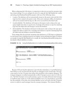
sufficiently to satisfy setup time requirements. This is illustrated in Figure 7.12
where the original clock signal, CLK, is reshaped using timing sets (TSETs) on the
tester. The rising edge can be delayed an arbitrary amount through use of the TSETs.
A rather simple way to accomplish this is to request, via the TSET, that the clock
signal be the complement of the value contained in the tester memory for the dura-
tion specified. Then, at the end of the elapsed period, CLK assumes the value con-
tained in pin memory.
Figure 7.11 Bidirectional I/O pad.
External
driver
I/O
pad
ts-enable
346
DEVELOPING A TEST STRATEGY
Figure 7.12 Shifting the clock edge.
Determining Which Vectors to Retain A typical design verification effort
may generate many millions of test sequences, far more than could possibly fit into a
typical tester memory. To select from these sequences a subset that provides good
coverage of physical defects in the design requires fault simulation. But, fault simu-
lation is a CPU intensive task. To perform a detailed fault simulation of all the
design verification suites can take an incredibly long time. To assist in the selection
process, two approaches can be employed: fault sampling and fault coverage pro-
files. We will now discuss each of these concepts in detail.
7.7.3 Fault Sampling
When a circuit is modeled at the gate level, the size of the fault list for that circuit,
after collapsing, is generally in the range of 2.5X, where X is the number of logic
gates. So, for example, a 100,000 gate circuit can be expected to have about 250,000
stuck-at faults in its fault list. If the objective is to sift through a large number of
design verification vector suites in order to find a subset that provides useful fault
coverage, then it is unnecessary to fault simulate the entire list of faults.
The practice of sampling can be put to good use in fault simulation. The object
is to evaluate the effectiveness of one or more sets of test vectors with the smallest
possible expenditure of CPU time, subject to the availability of main memory.
When designers are generating many hundreds or thousands of test programs,
often simulating them on specialized hardware simulators or emulators, over a
period of several months, it is not practical to fault simulate all of the sequences in
detail.
Fault sampling selects a subset of a total fault population for consideration during
fault simulation. The goal is to quickly get a reasonably accurate estimate of the
fault coverage produced by a set of test vectors. We consider here the development
provided by Wadsack.
13
Consider a population of N faults and a test that can detect
m of those faults. Assume that n out of N faults will be simulated. Let f = m/N and
F = X/n, where X is the number of faults detected from the random sample. Then f is
the actual fault coverage and F is an approximation of f based on the sample. The
variance of F is shown to be
CLK
0 100 200 300
T1 T2
CLKD
Var F() 1 nN⁄–()f 1 f–()1 n⁄()⋅⋅ ⋅=
THE FAULT SIMULATOR
347
A 95% confidence level is twice the square root of the variance, so f = F ± 2(Var(F))
1/2
.
The graph in Figure 7.13 shows the variance for a 10% sample when N = 100,000. This
graph reveals that the fractional error Z is likely to be less than 1%. Furthermore, the
error is greatest at a coverage of 50% and approaches 0 as the fault coverage
approaches 100%.
7.7.4 Fault-List Partitioning
Fault simulation can be extremely memory intensive, particularly when event-
driven, full-timing, concurrent fault simulation is being performed on a large cir-
cuit. It is often the case that complete fault simulation of an entire fault set for large
circuits simply is not possible due to insufficient memory. In such cases, the set of
faults can be partitioned into several smaller sets and each fault set can be simulated
individually. The results can be used to update a master fault list. If a fault list is
partitioned into, say, 10 subsets, each containing 10% of the faults from a master
fault list, then 10 passes will be required to completely fault simulate all of the sub-
sets. If each of the subsets is a pseudo-random selection of faults, without replace-
ment, from the master fault list, then the fault coverage percentage from each of
these partitions should be approximately the same, as discussed in the preceding
subsection. If the fault partition is made up of faults, all selected from the same
functional area of the IC, then the fault coverage from these partitions can show
substantial variation.
Fault partition sizes can be determined by the fault simulator. The operating sys-
tem can advise as to how much memory is available to keep track of fault effects.
The size of the data structure used to record fault effects is known and, with experi-
ence, a reasonably accurate estimate can be made of the number of fault effects that
exist, on average, for each fault origin. With this information, it is possible to esti-
mate how many faults can be processed in each fault simulation pass. If the esti-
mate is too optimistic, and not enough memory exists to process all of the faults,
then some of the faults can be deleted and fault simulation can continue with the
reduced fault list. Those faults that were deleted can be added back in a subsequent
fault partition.
Figure 7.13 Ninety-five percent confidence interval.
0.0 0.2
0.002
0.000
1.0
0.004
0.60.4 0.8
0.006
0.008
0.010
Z - Fractional error
F - Sample fault coverage
348
DEVELOPING A TEST STRATEGY
7.7.5 Distributed Fault Simulation
Distributed fault simulation can be part of a comprehensive strategy in which the
initial goal is to find a set of test programs that achieve high fault coverage, using
fault sampling techniques. After there is some degree of confidence that the test pro-
grams produce high coverage, then a complete fault simulation of all faults from a
master fault list can be performed, and the results can then be gathered up by the
control program. If, at this point, the fault coverage is still marginally below that
level needed to achieve a corporate AQL (acceptable quality level), then additional
test programs, or perhaps some DFT, can be used to reach the target fault coverage
level. In fact, this may be a critical juncture at which to make a decision as to
whether or not the use of design verification vectors should be abandoned and
replaced with a different test strategy, such as a full DFT. The decision might be
made because the coverage goals cannot be achieved otherwise, or the decision
might be made because the cost of testing each chip (time on the tester) may be too
great.
When a fault list is partitioned, individual partitions can be run serially, on the
same workstation, or they can be run in parallel over a network. A control program
running on a master workstation can spawn subordinate processes on other worksta-
tions connected via the network. When these subordinate processes finish, they
report their results to the control program, and the results are used to update a master
fault list. These subordinate processes can be run as background tasks with low pri-
ority so that if a user is working interactively on a workstation, for example, editing
a file, the subordinate process will not interfere with his or her activities.
7.7.6 Iterative Fault Simulation
During design verification, a common practice is to generate multiple files of stim-
uli. Each such file will be targeted at a specific area of the design, and these files
may be created by different designers. There is often overlap between these files. If
these files are to be used as part of the test program, then a common practice is to
iterate through these files and determine how much coverage is provided by each of
the design verification suites. With a large number of these design verification suites,
it is not uncommon to see that some suites will provide significant coverage, while
others may provide either very little coverage or perhaps no additional coverage.
If some suites provide very little coverage, then a decision must be made as to
whether or not the use of those suites is justified. Their contribution to overall
improvement in AQL may be negligible, while the test may contain so many vectors
as to add a significant amount of time on the tester. A strategy that may prove useful
is to fault simulate all of the design verification suites with a sample, say 10%, of the
fault set. Toss out the suites that provide no additional coverage, then rank the
remaining suites based on how much fault coverage they contribute to the total and
resimulate. Some of the suites that had very low coverage during the first iteration
may now drop out completely. This is essentially a covering operation, and it does
not improve the fault coverage; the same faults will be detected, assuming the same
fault sample is used, but the objective is to find the smallest set of suites that achieve
THE FAULT SIMULATOR
349
that fault coverage, hence the smallest number of vectors, thus reducing the amount
of time the device spends on the tester.
7.7.7 Incremental Fault Simulation
Incremental fault simulation permits the user to conditionally create and apply stim-
uli to the circuit. These stimuli may be experimental. For example, the user may be
trying to drive the circuit into a particular state in order to sensitize a group of faults
that would otherwise go undetected. In order to achieve the goal, the user must be
able to apply the stimuli and monitor response, including internal states of the cir-
cuit. In the event that stimuli do not achieve their desired end, it is also necessary, to
be able to delete some or all of the stimuli. This implies an ability to checkpoint the
circuit, and to back up to that checkpoint if analysis of simulation results identifies
incorrect state transitions or some other reason for failure to improve fault coverage.
7.7.8 Circuit Initialization
Indeterminate states at the beginning of a simulation present a significant problem
for fault simulators. Some designs, in particular those that take advantage of DFT
structures, are able to initialize some or all of the circuit storage elements quite
quickly, often simply by toggling a reset input. However, there are circuits that
require complex sequences to drive all of the flip-flops and latches into a known
state. Many fault detections during this initialization period are probable detects, in
which the good circuit has a known value e ∈ {0,1}, and the faulty circuit has an
unknown value, X. This composite signal e/X may propagate to an output where it is
recorded as a probable detect. In this case, the response for the fault-free circuit is
known, but the response for the faulty circuit has, on average, only a 50% probabil-
ity of possessing a binary value that is different from the good circuit. A problem
with probable detects is the fact that many applications require absolute detections,
particularly in products where health or public safety are at risk. The probable detect
may cause the fault simulator to ignore later absolute fault detects, thus obscuring
the true fault coverage.
One way to deal with this is to simply ignore faults detected at the I/O pins until
initialization is complete. However, this does not resolve the problem of probable
detects. Suppose a reset input on a flip-flop is stuck to the inactive state. Then, in a
concurrent fault simulator, the fault origin will spawn fault effects (cf. Section 3.7.2)
that will reach an I/O pin, where they will be ignored until the fault simulator is told
to begin recording detected faults.
An alternate approach is for the fault simulator to be configured to postpone
propagation of fault effects until the circuit has reached a known state. Then, after
the circuit has been initialized, if a flip-flop output switches from 0 to 1 (1 to 0), and
if that transition causes a transition on an output, then a fault on, for example, the
clock line would prevent the transition from occurring, and the observable signal
would appear stable at the output when it should be switching. Thus, faults can be
detected with certainty. In this arrangement it is possible that faults may actually be
350
DEVELOPING A TEST STRATEGY
detected sooner on the tester. But they could only be recorded as a probable detect
by the fault simulator. This strategy requires the user to create an initialization
sequence that fully initializes the circuit.
An alternate strategy for getting a full and accurate tabulation of faults that are
absolute detects, and those that are only probable detects, is to run fault simulation
twice. During the first run, fault simulation is configured to count only absolute
detections. Then, on a final run, fault simulation is run with all the undetected faults,
but it is configured to count probable detects. It may then be possible to set a thresh-
old, requiring that a fault be counted as a probable detect if it is detected some mini-
mum number of times. In commercial products, a default of five or ten probable
detects is often set as a default.
7.7.9 Fault Coverage Profiles
For many years, fault simulation simply consisted of generating lists of faults, col-
lapsing the lists, and then running one or more files of test vectors against the netlist
and fault list to determine fault coverage provided by the set(s) of test vectors. If
fault coverage was satisfactory, their job was done. But, if fault coverage was unsat-
isfactory, engineers writing additional test vectors to improve fault coverage fre-
quently would work in the blind. It was possible to get a list of detected and
undetected faults, but the data were simply too overwhelming to be of any value.
The fault coverage profiler, or reporter, as it is sometimes called, is a data reduction
tool. It enables the user to generate detailed reports on fault coverage.
An overall fault coverage of 90% for an IC is a composite of fault coverages for
many smaller functions that make up the design. For example, a 90% fault coverage
for a microprocessor is a composite fault coverage over control logic, ALU, inter-
rupt control, I/O control, and so on. It is not uncommon for individual fault cover-
ages to vary over a wide range. In fact, it would be unusual if fault coverages for
different parts of a design were all within one or two percentage points of the com-
posite fault coverage.
The profiler reads the master fault file and extracts results for modules identified
by the user. For example, the interrupt logic in a microprocessor might be spread
across several submodules grouped together under a top-level module identified as
INT. The user can request fault coverage statistics for INT and for all submodules
contained in INT. Alternatively, the user may request that the profiler list only the
undetected faults in that section of logic.
If fault coverage for a particular module is unsatisfactory, the user can request a
further breakdown. Suppose that a microprocessor contains a register bank made up
of 16 registers, and that a small subset of them were used constantly during design
verification, to the exclusion of all other registers. A fault coverage profile will
reveal that the register bank has unacceptably low fault coverage. A further request
for more details from the profiler can give additional details, showing fault coverage
for each individual register. Being able to zoom in and spot those precise functions
that have poor coverage is a significant productivity enhancer. Rather than blindly
create test vectors and fault simulate in the hopes that fault coverage will improve,
THE FAULT SIMULATOR
351
the profiler makes it possible to explore specific areas of a design and identify those
in need of improvement.
Knowing where undetected faults reside sometimes is enough to improve cover-
age with minimal effort. Consider the aforementioned register bank. If for some rea-
son they are overlooked during generation of a test, the profiler can reveal that fact
immediately and, once it known, all that is required is that load and store instruc-
tions be executed to test these registers. The fault coverage is then improved with
negligible effort. An important side effect of this strategy is a higher quality test. It
has been reported that a test in which several functions have approximately equal
coverage will generally experience fewer tester escapes than another test with the
same total fault coverage, but with the coverage more unevenly distributed across
the modules.
14
7.7.10 Fault Dictionaries
During fault simulation it is common for several faults to be detected by each test
pattern. When testing a printed circuit board it is desirable to isolate the cause of an
erroneous output to as small a group of candidate faults as is practical. Therefore,
rather than stop on the first occurrence of an output error and attempt to diagnose the
cause of an error, a tester may continue to apply patterns and record the pattern num-
ber for each failing test pattern. At the conclusion of the test, the list of failed pat-
terns can be used to retrieve diagnostic data that identifies potential faults detected
by each applied pattern. If one or more faults are common to all failed patterns, the
common faults are high-probability candidates.
To assist in identifying the cause of an erroneous response, a fault dictionary can
be used. A fault dictionary is a data file that defines a correspondence between faults
and symptoms. It can be prepared in several ways, depending on the amount of data
generated by the fault simulator.
15
If the ith fault in a circuit is denoted as F
i
, then a
set of binary pass–fail vectors F
i
= ( f
i1
, f
i2
, . . ., f
in
) can be created, where
These vectors can be sorted in ascending or descending order and stored for fast
retrieval during testing. During testing, if errors are detected, a pass–fail vector
can be created in which position i contains a 1 if an error is detected on that pat-
tern and a 0 if no error is detected. This vector is compared to the pass–fail vectors
created from simulation output. If one, and only one, vector is found to match the
pass–fail vector resulting from the test, then the fault corresponding to that pass–
fail vector is a high-probability fault candidate. It is possible of course that two or
more nonequivalent faults have the same pass–fail vector, in which case it is possi-
ble to distinguish between them only if they have different symptoms; that is, they
fail the same test pattern numbers but produce different failing responses at the
output pins.
f
ik
1iff
i
is detected by test T
k
0 otherwise
=