Bio-MEMS Technologies and Applications - Wang and Soper (Eds) Part 4 doc
Bạn đang xem bản rút gọn của tài liệu. Xem và tải ngay bản đầy đủ của tài liệu tại đây (402.04 KB, 17 trang )
The LIGA Process 83
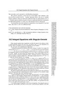
Key advantages of LIGA-made microstructures are the inherent precision
and the ability to cover lateral dimensions from submicrometer to millimeter
sizes. These features make LIGA microstructures valuable for integrating
assembly and packaging features into MEMS devices, and drastically mini-
mizing the overall packaging effort, a huge cost factor in MEMS devices.
The molding process especially can be flexibly combined, for example with
Si-based microelectronics on the batch/wafer level, further improving sys-
tem integration and high-yield production and reducing overall device
assembly efforts. Research in LIGA is an ongoing, active field and a number
of new ideas combined with novel materials prove that LIGA technologies
still spark the interest and excitement of the research community. These
efforts are often driven by concrete requirements for new MEMS applications
from industrial partners. A remaining challenge for LIGA is the lack of
standardized processes demanding reevaluation and optimization of process
details for nearly every new microstructure. This also slows down the tran-
sition into commercial manufacturing.
In conclusion, LIGA technology has matured to the point that commercial
applications have become possible and are being pursued. Applications
including bio-MEMS and microfluidics have moderate structure require-
ments but need cost-effective production and dedicated materials to meet
market demands. A number of alternative microfabrication technologies,
including precision micromachining and micro-EDM are employed for mold
insert fabrication, and molding becomes the manufacturing technology of
choice for the microparts. A direct-LIGA approach combining x-ray lithog-
raphy and electroplating is used for applications for microstructures with
extreme precision and very high aspect ratios. Prototype fabrication of these
structures can be satisfied but scaling-up production with high yield and
high quality remains a challenge for the future.
Acknowledgment
Thank you to Prof. Wanjun Wang (LSU-ME department) for his support with
the electroplating section and editing of the overall text, Proyag Datta
(research associate at CAMD) for contributions to the molding chapter, and
Jens Hammacher for his assistance in preparing some of the figures. I also
appreciate contributions from Professor Kevin Kelly (LSU-ME department
and founder, Mezzo International, Inc.) on LIGA applications for the regen-
erator and heat exchanger, and Dr. Todd Christenson, HT Micro Analytical,
Inc., for commercial examples of LIGA structures in precision engineering
and micro-optics. Last, but not least, I would like to acknowledge the many
publications written by former and current colleagues and friends who are
DK532X_book.fm Page 83 Friday, November 10, 2006 3:31 PM
© 2007 by Taylor & Francis Group, LLC
84 Bio-MEMS: Technologies and Applications
using LIGA technologies in their MEMS research and whose work I have
included in this chapter.
References
[1] Becker, E.W., Ehrfeld, W., Münchmeyer, D., Belz, H., Heuberger, A., Pongratz,
S., Glashauser, W., Michel, H.J., and Siemens, R., Production of separation-
nozzle systems for uranium enrichment by a combination of x-ray lithography
and galvanoplastics, Naturwissenscahften 69 (1982), 520–523.
[2] Becker, E.W., Ehrfeld, W., Münchmeyer, D., Hagmann, P., and Maner, A Fab-
rication of microstructures with high aspect ratios and great structural heights
by synchrotron radiation lithography, galvanoforming and plastic moulding
(LIGA process), Microelectronic Engineering 4, (1986), 35–56.
[3] Kendall, D.L. and Shoultz, R.A., in SPIE Handbook of Microlithography, Micro-
machining, and Microfabrication, Vol. II, Rai-Choudhury, P., Ed. (1997), 41–98.
[4] Pang, S.W., in SPIE Handbook of Microlithography, Micromachining, and Microfab-
rication, Vol. II, Rai-Choudhury, P., Ed. (1997), 99–152.
[5] Hormes, J., Goettert, J., Lian, K., Desta, Y.M., and Jian, L., Materials for LiGA
and LiGA-based Microsystems, Nuclear Instruments and Methods in Physics Re-
search, B 199 (2003), 332–341.
[6]
[7] Friedrich, C., Warrington, R., Bacher, W., Bauer, W., Coane, P., Göttert, J., Hane-
mann, T., Hausselt, J., Heckele, M., Knitter, R., Mohr, J., Piotter, V., Ritzhaupt-
Kleissl, H J., and Ruprecht, R., in SPIE Handbook of Microlithography, Microma-
chining, and Microfabrication, Vol. II, Rai-Choudhury, P., Ed. (1997), 299–377.
[8] Hruby, J., LIGA technologies and applications, MRS Bulletin 26, 4 (2001),
337–340.
[9] Arendt, M., Meyer, P., Saile, V., and Schulz, J., Launching into a golden age
(1)—marketing strategy for distributed LIGA-fabrication, Proceedings of the 10th
International Conference on Commercialization of Micro and Nano Systems (COMS
2005), Baden-Baden, August 21–25, 2005, MANCEF, Albuquerque, NM.
[10] Hahn, L., Meyer, P., Bade, K., Hein, H., Schulz, J., Löchel, B., Scheunemann,
H.U., Schondelmaier, D., and Singleton, L. MODULIGA: The LIGA process as
a modular production method-current standardization status in Germany, Mi-
crosystems Technologies 11 (2005) S.240–245.
[11] Malek, C.K. and Saile, V., Applications of LIGA technology to precision man-
ufacturing of high-aspect-ratio micro-components and -systems: A review, Mi-
croelectronics Journal 35 (2004), S.131–143.
[12] Hruby, J.M., LIGA technologies and applications, MRS Bulletin 26, 4 (2001),
337–340.
[13] Jian, L., Desta, Y.M., Aigeldinger, G., Bednarzik, M., Goettert, J., Loechel, B.,
Jin, Y., Singh, V., Ahrens, G., Gruetzner, G., Ruhmann, R., and Degen, R., SU-
8 based deep x-ray lithography/LIGA, Proc. SPIE (International Society for
Optical Engineering) 4979 (2003), 394–401.
[14] Koch, E.E., Ed., Handbook on Synchrotron Radiation, Vols. 1–3, North-Holland,
Amsterdam (1983).
DK532X_book.fm Page 84 Friday, November 10, 2006 3:31 PM
HT Micro, . Accessed August 14, 2006.
© 2007 by Taylor & Francis Group, LLC
The LIGA Process 85
[15]
[16] More details on the properties of synchrotron radiation are available in the
following sources: Saile, V., Properties of synchrotron radiation, in Vorlesungs-
manuskript of the 23. IFF-Ferienkurs, Forschungszentrum Jülich (1992), 1.1–28;
Handbook on Synchrotron Radiation, Vol. 1, edited by E.E. Koch, North-Holland,
Amsterdam (1983).
[17] A good summary of the history of x-ray lithography for VLSI application is
presented in the IBM Journal of Research and Development 37, 3 (1993), 287–474.
[18] Cerrina, F., X-ray lithography, in SPIE Handbook of Microlithography, Microma-
chining, and Microfabrication, Vol. I, Rai-Choudhury, P., Ed. (1997), 251–319.
[19] Kempson, V.C. et al., Experience of routine operation of Helios 1, EPAC (1994),
594–596.
[20] Ehrfeld, W.; Bley, P., Goetz, F., Mohr, J., Muechnmeyer, D., and Schelb,
W., Progress in deep-etch synchrotron radiation lithography, J. Vac. Sci. Technol.
B 6, 1 (1988), 178–182.
[21] Christenson, T., X-ray based fabrication, Micro/Nano R&D Magazine 10, 10
(2005), 1–2.
[22]
14, 1996.
[23]
August 14, 1996.
[24]
gust 14, 1996.
[25]
tails about the LIGA activities are summarized under “Microfabrication”; tech-
nical details on beamlines and scanners are discussed under “Beamlines.”
[26] Griffiths, S., Hruby, J., and Ting, A., The influence of feature sidewall tolerance
on minimum absorber thickness for LIGA x-ray masks, J. Micromech. Microeng.
9 (1999), 353–361.
[27] Chen, Y., Kupka, R.K., Rousseaux, F., Carcenac, F., Decanini, D., Ravet, M.F.,
and Launois, H., 50 nm x-ray lithography using synchrotron radiation, J. Vac.
Sci. Technol. B 12, 6 (1994), 3959–3964.
[28] Schomburg, W.K., Baving, H.J., and Bley, P., Ti-and Be-x-ray masks with align-
ment windows for the LIGA process, Microelectronic Engineering 13 (1991),
323–326.
[29] Klein, J., Guckel, H., Siddons, D.P., and Johnson, E.D., X-ray masks for very
deep x-ray lithography, Microsystems Technologies 4 (1998), 70–73.
[30] Coane, P., Giasolli, R., Ledger, S., Lian. K., Ling, Z., and Göttert, J., Fabrication
of HARM structures by deep x-ray lithography using graphite mask techno-
logy, Microsystem Technologies 6 (2000), 94–98.
[31] Desta, Y. et al., Fabrication of graphite masks for deep and ultra-deep x-ray
lithography, Proc. SPIE (International Society for Optical Engineering) 4175,
(2000).
[32] Desta, Y. et. al., X-ray masks for the LIGA process, HARMST 2003, Monterey,
CA, June 2003.
[33] Wang, L., Desta, Y.M., Fettig, R.K., Goettert, J., Hein, H., Jakobs, P., and Schulz,
J High resolution x-ray mask fabrication by a 100 keV electron-beam lithog-
raphy system, J. Micromech. Microeng. 14 (2004), S.722–726.
DK532X_book.fm Page 85 Friday, November 10, 2006 3:31 PM
Advanced Light Source, list of synchrotron sources, />als/synchrotron_sources.html. Accessed August 14, 2006.
BESSY Anwenderzentrum, Accessed August
ANKA GmbH, Accessed
IMT at Forschungszentrum Karlsruhe, Accessed Au-
For more details visit the CAMD homepage De-
© 2007 by Taylor & Francis Group, LLC
86 Bio-MEMS: Technologies and Applications
[34] Mohr, J., Ehrfeld, W., and Münchmeyer, D., Analyse de Defektursachen und
der strukturvebertragung bei der Roentgentiefenlithographie mit synchrotron-
strahlung, KfK Report 4414, Forschungszentrum Karlsruhe (1988).
[35] Guckel, H. et al., U.S. patent # 5378583 (1995).
[36] Bernhardt, D., Fabrication and structure-analysis of ultra-tall HARM made in
SU-8 and PMMA, master’s thesis, Fachhochschule Gelsenkirchen, February 2004.
[37] Becnel, C., Desta, Y., and Kelly, K., Ultra-deep x-ray lithography of densely
packed SU-8 features (parts I & II), J. Micromech. Microeng. 6 (2005), 1242.
[38] Schnabel, W., Polymer Degradation—Principles and Practical Applications,
Hanser, Munich (1981).
[39] Levinson, H.J. and Arnold, W.H. Optical lithography, in SPIE Handbook of
Microlithography, Micromachining, and Microfabrication, Vol. I Rai-Choudhury, P.,
Ed., (1997), 11–138, SPIE Press, Bellingham, WA.
[40] Meyer, P., Schulz, J., and Hahn L., DoseSim: Microsoft-Windows graphical user
interface for using synchrotron x-ray exposure and subsequent development
in the LIGA process, Review of Scientific Instruments 74 (2003), S.1113–1119.
[41] Maid, B., Ehrfeld, W., Hormes, J., Mohr, J., and Muechmeyer, D., Adaptation of
Spectral Distribution of Synchrotron Radiation to x-ray Depth Lithography, KfK
Report 4579 (1988), Forschungszentrum Karlsruhe, Karlsruhe, Germany.
[42] Jian, L., Desta, Y.M., Goettert, J., Multi-level microstructures and mold inserts
fabricated with planar and oblique x-ray lithography of SU-8 negative photo-
resist, Proc. SPIE (International Society for Optical Engineering) 4557 (2001),
69–76.
[43] Reznikova, E.F., Mohr, J., and Hein, H. Deep photo-lithography characteriza-
tion of SU-8 resist layers, Microsystems Technologies 11 (2005), 282–291.
[44] Goettert, J., Ahrens, G., Bednarzik, M., Degen, R., Desta, Y.M., Gruetzner, G.,
Jian, L., Loechel, B., Ruhmann, R., and Jin, Y., Cost effective fabrication of high
precision microstructures using a direct-LIGA approach, Proc. COMS (2002),
Ypsilanti, Michigan, September 2002.
[45] Dentinger, P.M., Clift, W.M., and Goods, S.H., Removal of SU-8 Photoresist for
thick film application, Microelectronic Engineering 61–62 (2002), 993–1000.
[46] Feiertag, G., VDI Report 242, Röntgenticfenlithographische Mikrostruktur-fer-
tigung, Düsseldorf (1996).
[47] Feiertag G., Ehrfeld, W., Lehr, H., Schmidt, A., and Schmidt, M., Accuracy of
structure transfer in deep x-ray lithography, J. Microelectronic Eng. 35 (1997),
557–560.
[48] Feiertag, G., Ehrfeld, W., Lehr, H., Schmidt, A., and Schmidt, M., Calculation
and experimental determination of the structure transfer accuracy in deep x-
ray lithography, J. Micromech. Microeng. 7 (1998), 323–331.
[49] Aigeldinger, G., Implementation of an ultra deep x-ray lithography system at
CAMD, Ph.D. thesis, University of Freiburg, 2001.
[50] Münchmeyer, D., Ehrfeld, W., and Becker, E.W., KfK Report 3732, Untersuchun-
gen zur Abbildungenauigket der Röntgentiefen lithografie mit synchrotron-
strah-lung bei der Hersellung Technischer Trennduesen, Forschungszentrum
Karlsruhe (1984).
[51] Pantenburg, F.J. and Mohr, J., Influence of secondary effects on the structure
quality in deep x-ray lithography, Nuclear Instruments and Methods in Physics
Research B 97 (1995), 551–556.
[52] Griffiths, S.K., Fundamental limitations of LIGA x-ray lithography: Sidewall off-
set, slope and minimum feature size, J. Micromech. Microeng. 14 (2004), 999–1011.
DK532X_book.fm Page 86 Friday, November 10, 2006 3:31 PM
© 2007 by Taylor & Francis Group, LLC
The LIGA Process 87
[53] Zumaqué Diaz, H., Zur auflösungsreduzierenden sekundärstrahlung in der
Röntgentiefenlithographie, Ph.D. thesis, University of Bonn BONN-IR-98-N,
(1998).
[54] Pantenburg, F.J., Chlebek, J., El-Kholi, A., Huber, H L., Mohr, J., Oertel, H.K.,
and Schulz, J., Adhesion problems in deep-etch x-ray lithography by fluores-
cence radiation from the plating base; Microelectronic Engineering 23 (1994),
223–226.
[55] Griffiths, S.K. and Ting, A., The influence of x-ray fluorescence on LIGA side-
wall tolerances, Microsystems Technologies 8 (2002), 120–128.
[56] Achenbach, S., Pantenburg, F.J., and Mohr, J., Numerical simulation of thermal
distortions in deep and ultra deep x-ray lithography, Microsystems Technologies
9 (2003), 220–224.
[57] Achenbach, S., Pantenburg, F.J., and Mohr, J., Optimization of the Process Condi-
tions for the Fabrication of Microstructures by Ultra Dep X-Ray Lithography
(UDXRL), FZKA Report 6576 (2000), Forschungszentrum, Karlsruhe, Germany.
[58] Tabata, O., You, H., Matsuzuka, N., Yamaji, T., Uemura, S., and Dama, I.,
Moving mask deep x-ray lithography system with multi stage for 3-D micro-
fabrication, Microsystem Technologies 8 (2002), 93–98.
[59] Burbaum, C. and Mohr, J., Herstellung von mikromechanischen Beschleunigungs-
sensoren in LIGA-Technik, KfK Report 4859 (1991), Forschungszentrum, Karlsru-
he, Germany.
[60] Strohrmann, M., Mohr, J., and Schulz, J., Intelligent Microsystem for Acceleration
Measurement Based on LIGA Micromechanics, FZKA Report 5561 (1995), Fors-
chungszentrum, Karlsruhe, Germany.
[61] Zanghellini, J., El-Kholi, A., and Mohr, J., Development behavior of irradiated
microstructures, Microelectronic Engineering 35 (1997), 409–412.
[62] Zanghellini, J., Achenbach, S., El-Kholi, A., Mohr, J., and Pantenburg, F.J., New
development strategies for high aspect microstructures, Microsystems Technol-
ogies 4 (1998), 94–97.
[63] Nilson, R.H., Griffiths, S.K., and Ting, A., Modeling acoustic agitation for en-
hanced development of LIGA resists, Microsystems Technologies 9 (2002),
113–118.
[64] Griffiths, S.K., Crowell, J.A.W., Kistler, B.L., and Dryden, A.S., Dimensional
errors in LIGA-produced metal structures due to thermal expansion and swell-
ing of PMMA, J. Micromech. Microeng., 8 (2004), 1548–1557.
[65] Schlesinger, M. and Paunovic, M., Eds., Modern Electroplating, John Wiley &
Sons, New York (2000).
[66] Bacher, W., Bade, K., Leyendecker, K., Menz, W., Stark, W., and Thomes, A.,
Electrodeposition of microstructures: An important process in microsystem
technology, in Electrochemical Technology: Innovations and New Developments,
Masuko, N., Osaka, T., and Ito, Y., Eds., Kodansha, Tokio (1996), 159–189.
[67] Cho, H.S., Hemker, K.J., Lian, K., Goettert, J., and Dirras, G., Measured me-
chanical properties of LIGA Ni structures, J. of Sensors and Actuators A 103
(2003), 59–63.
[68] Yang, N.Y.C., Headley, T.J., Kelly, J.J., and Hruby, J.H., Metallurgy of high
strength Ni-Mn microsystems fabricated by electrodeposition, Scripta Materialia
51 (2004), 761–766.
[69] Dukovic, J. and Tobias, C.W., Influence of attached bubbles on potential drop
and current distribution at gas-evolving electrodes, Journal of the Electrochemical
Society 134 (1987), 331–343.
DK532X_book.fm Page 87 Friday, November 10, 2006 3:31 PM
© 2007 by Taylor & Francis Group, LLC
88 Bio-MEMS: Technologies and Applications
[70] Romankiw, L.T. and O’Sullivan, E.J.M., Plating techniques, in SPIE Handbook
of Microlithography, Micromachining, and Microfabrication, Vol. II, Rai-Choudhury,
P., Ed. (1997), 197–298.
[71] Okinaka, Y. and Wolowodiuk, C., Cyanoaurate(III) formation and its effect on
current efficiency in gold plating, Journal of the Electrochemical Society 128 (1981),
288–294.
[72] Baudrand, D.W. and Mandich, N.V., Troubleshooting electroplating installa-
tions: Nickel sulfamate plating system, Plating and Surface Finishing 89 (2002),
68–76.
[73] Tsuru, Y., Nomura, M., and Foulkes, F.R., Effects of boric acid on hydrogen
evolution and internal stress in films deposited from a nickel sulfamate bath,
Journal of Applied Electrochemistry 32 (2002), 629–634.
[74] Saito, T., Sato, E., Matsuoka, M., and Iwakura, C., Electroless deposition of Ni-
B, Co-B and Ni-Co-B alloys using dimethylamineborane as a reducing agent,
Journal of Applied Electrochemistry 28 (1998), 559–563.
[75] Okinaka, Y., Koch, F.B., Wolowodiuk, C., and Blessington, D.R., Left double
quote polymer right double quote inclusions in cobalt-hardened electroplated
gold, Journal of the Electrochemical Society 125 (1978), 1745–1750.
[76] Schlesinger, M. and Paunovic, M., Electrochemical Engineering Principles, Prentice
Hall, Englewood Cliffs, New Jersey (1991).
[77] Mandich, N.V., pH, hydrogen evolution and their significance in electroplating
operations, Plating and Surface Finishing 89 (2002), 54–58.
[78] Harper, C.A., Ed., Modern Plastics Handbook, McGraw Hill, New Delhi (2000).
[79] Matthew, H. and Naitove, M.H., Close up on Technology: Mold simulation
[80] Heckele, M. and Schomburg, K.W., Review on micro molding of thermoplastic
polymers, J. Micromech. Microeng., 14 (2004), R1–R14.
[81] Rowland, H.D., Polymer deformation and filling modes during microemboss-
ing, J. Micromech. Microeng. 14 (2004), 1625–1632.
[82] Schift, H. et al., Pattern formation in hot embossing of thin polymer films,
Nanotechnology 12, 2 (2001), 173–177.
[83] Rupreccht, R., Bade, K., Bauer, W., Baumeister, G., Hanemann, T., Heckele, M.,
Holstein, N., Merz, L., Piotter, V., and Truckenmueller, R., Micro Replication in
Polymers, Metals, and Ceramics, FZKA Report 6990 (2004), 95–102, Forschung-
szentrum, Karlsruhe, Germany.
[84] Worgull, M. and Heckele, M., New aspects of simulation in hot embossing,
Microsystem Technologies 10, 5 (2004), 432–437.
[85] Michel, A., Ruprecht, R., Harmening, M., and Bacher, W., Abformung von Mik-
rostrukturen auf prozessierten Wafern, KfK Report 5171 (1993), Forschungszen-
trum, Karlsruhe, Germany.
[86] Otto, T. et al., Fabrication of micro optical components by high precision em-
bossing, Proc. SPIE (International Society for Optical Engineering) 4179 (2000),
96–106.
[87] Heckele, M. and Bacher, W., FZKA Report 6080 (1998), 89–94, Forschungszen-
trum, Karlsruhe, Germany.
[88] Müller, A., Göttert, J., Mohr, J., and Rogner, A., Microsystem Technologies 2 (1996),
40–45.
[89] Larsson, O., Ohman, O., Billman, A., Lundbladh, L., Lindell, C., and Palmskog, G.,
Proc. Transducer ’97 (1997), 1415–1418, Forschungszentrum, Karlsruhe, Germany.
DK532X_book.fm Page 88 Friday, November 10, 2006 3:31 PM
mold analysis gets faster, easier, smarter, Plastics Technology, http://www
.plasticstechnology.com/articles/200602cu1.html.
© 2007 by Taylor & Francis Group, LLC
The LIGA Process 89
[90] Ruther, P., Gerlach, B., Göttert, J., Ilie, M., Mohr, J., Müller, A., and Ossmann,
C., Pure and Applied Optics 6 (1997), 643–653.
[91] Kim, J H. and Neyer, A., J. Opt. Commun. 17 (1996), 172–178, Forschungszen-
trum, Karlsruhe, Germany.
[92] Müller, C. and Mohr, J., FZKA Report 5609, Forschungszentrum Karlsruhe
(1995), Forschungszentrum, Karlsruhe, Germany.
[93] Both, A., Bacher, W., Heckele, M., and Ruprecht, R., Herstellung beweglicher
LIGA-Mikrostrukturen durch positionierte Abformung, FZKA Report 5671 (1995),
Forschungszentrum, Karlsruhe, Germany.
[94] Müller, K D., FZKA Report 6254, Forschungszentrum Karlsruhe (1999), Fors-
chungszentrum, Karlsruhe, Germany.
[95] Strohrmann, M., Bley, P., Fromheim, O., and Mohr, J., Sensors & Actuators A
41–42 (1994), 426ff.
[96] Guber, A.E. et al., Microfluidic lab-on-a-chip systems based on polymers—fab-
rication and application, Chemical Engineering Journal 101, 1–3 (2004), 447–453.
[97] Kricka, L.J. et al., Fabrication of plastic microchips by hot embossing, Lab on a
Chip 2, 1 (2002), 1–4.
[98] One example of a commercial microfluidic lab chip is the Caliper LabCard
TM
.
[99] Fatikow, S., Microrobots take on microassembly tasks, MST News 22 (1997), 20–26.
[100] Woellmer, H., Precision casting of metal microparts, FZKA Nachrichten, 3–4
(1998), 237–242.
[101] Bauer, W. and Knitter, R., Shaping of ceramic microcomponents, FZKA Nach-
richten 3–4 (1998), 243–250.
[102] Caesar, H.H., Dental-Labor 2 (1988), 189–193.
[103] Management Project Microsystems Technologies (PMT), FZK Karlsruhe, FZKA
Report 6080 (1998).
[104] Products for microfluidic, micro-optics, and life science applications are devel-
oped by Boehringer-Ingelheim within their microtechnology department (for-
[105] Products for thermal management applications including heat exchangers,
regenerators, and microreactor systems are developed by International Mezzo
[106] Products for microreactor technology, life sciences, and micro-optics are devel-
[107] Micromotion GmbH uses direct LIGA technology for fabricating miniaturized
®
gust 14, 2006.
[108]
Axsun Technologies offers LIGA services and produces miniaturized optical
14, 2006.
[109] Polymicro represents a group of research institutes and industry members
offering micro-optics components and systems made by replication techniques
[110] Bley, P., Goettert, J., Harmening, M., Himmelhaus, M., Menz, W., Mohr, J.,
Müller, C., and Wallrabe, U., The LIGA process for the fabrication of microme-
chanical and micro-optical vomponents, in Micro System Technologies 91, Reichl,
H., Ed., Springer, Berlin (1991).
DK532X_book.fm Page 89 Friday, November 10, 2006 3:31 PM
For more details see />merly microParts GmbH), />mikrosystemtechnik/microtechnology/index.jsp. Accessed August 14, 2006.
Systems, Accessed August 14, 2006.
oped and commercialized at the Institut fuer Mikrotechnik Mainz, http://
www.imm-mainz.de/. Accessed August 14, 2006.
Harmonic Drive Gear systems,
Accessed Au-
systems for sensor applications, Accessed August
in polymers. Accessed August 14, 2006.
© 2007 by Taylor & Francis Group, LLC
90 Bio-MEMS: Technologies and Applications
[111] Mohr, J., Goettert, J., Müller, A., Ruther, P., and Wengeling, K., Micro-optical
and optomechanical systems fabricated by the LIGA technique, Photonics West
’97, Proc. SPIE (International Society for Optical Engineering) 3008 (1997),
273–278.
[112] Müller, A., Goettert, J., and Mohr, J., LIGA microstructures on top of microma-
chined silicon wafers used to fabricate a micro-optical switch, J. Micromech.
Mircoeng. 3 (1993), 158–160.
[113] Qi, S.Z., Liu, X.Z., Ford, S., Barrows, J., Thomas, G., Kelly, K., McCandless, A.,
Lian, K., Goettert, J., and Soper, S.A., Microfluidic devices fabricated in
poly(methyl methacrylate) using hot-embossing with integrated sampling cap-
illary and fiber optics for fluorescence detection, Lab on a Chip 2 (2002), 88–95.
[114] Bacher, W. et al., Fabrication of LIGA mold inserts, Microsystem Technologies 4,
3 (1998), 117–119.
[115] Datta, P. and Goettert, J., Methods for polymer hot embossing process devel-
opment, in Book of Abstracts, HARMST05, June 10–13, 2005, Gyeongju, Korea,
[116]
[117]
[118]
®
gust 14, 2006.
119.
Degen, R. and Slatter, R., Hollow shaft micro servo actuators realized with the
Micro†Harmonic†Drive
®
, Proceedings ACTUATOR2002, Bremen, June 2002.
[120]
14, 1996.
[121]
[122] Solutions for lab-on-a-chip applications using COC polymer chips are offered
[123]
[124] Fluidic chips (LabCard) and fluidic handling system for analytical applications
[125]
2
[126]
Datta, P., Hammacher, J., Pease, M., Gurung, S., and Goettert, J., Development
of an integrated polymer microfluidic stack, to be published in Proc. iMEMS
2006, Singapore, May 2006.
[127] Ackerman, R., Cryogenic Regenerative Heat Exchangers, Plenum Press, New York
(1997).
[128] Radebaugh, R. Foundations of Cryocoolers, Short course presented at the 12th
International Cryocooler Conference, MIT, Cambridge, MA, June 17, 2002.
[129] Schlossmacher, P., Yamasaki, T., Ehrlich, K., Bade, K., and Bacher, W., Produc-
tion and characterization of Ni-based alloys for applications in microsystems
technology, FZKA Nachrichten 30 Karlsruhe (1998), 207–214.
DK532X_book.fm Page 90 Friday, November 10, 2006 3:31 PM
MEMS Exchange, . Accessed August 14, 2006.
Micromotion GmbH uses direct LIGA technology for fabricating miniaturized
256–257, accepted for publication in Microsystem Technologies.
Nanoplex, />Harmonic Drive Gear systems,
Accessed Au-
BESSY Anwenderzentrum, Accessed August
MRT GmbH, Accessed August 14, 2006.
by Thinxxs, Germany; for more information visit their webpage at http://www
Solutions for microfluidic chips are available from microfluidic ChipShop; for
.thinxxs.com/.
details see their catalog at rofluidic-chipshop.com/index
.php?pre_cat_open=209.
are offered by Micronics Inc; for more details see their webpage at http://www
.micronics.net/. Accessed August 14, 2006.
Homepage CBM at
Accessed August 14, 2006.
© 2007 by Taylor & Francis Group, LLC
The LIGA Process 91
[130] Tkaczyk, T.S., Rogers, J.D., Rahman, M., Christenson, T.C., Gaalema, S., Dere-
niak, E.L., Richards-Kortum, R., and Descour, M.R., Multi-modal miniature
microscope: 4M device for bio-imaging applications—an overview of the sys-
tem, Proc. SPIE (International Society for Optical Engineering) 5959 (2005),
138–146.
[131] Rogers, J.D., Kärkkäinen, A., Tkaczyk, T.S., Rantala, J., and Descour, M.R.,
Realization of refractive micro-optics through grayscale lithographic patterning
DK532X_book.fm Page 91 Friday, November 10, 2006 3:31 PM
of photosensitive hybrid glass, Opt. Express 12 (2004), 1294–1303. http://
www.opticsinfobase.org/abstarct.cfm?URI=oe-12-7-1294.
© 2007 by Taylor & Francis Group, LLC
93
4
Nanoimprinting Technology
for Biological Applications
Sunggook Park and Helmut Schift
CONTENTS
4.1 Introduction 94
4.2 Overview of NIL Technology 95
4.2.1 NIL Process 95
4.2.2 Polymer Flow during NIL 97
4.2.3 Biocompatibility of the Resist 100
4.2.4 Stamps with Nanostructures 101
4.2.5 Antiadhesive Layer Coating 102
4.3 NIL in Biological Applications 103
4.3.1 Nanofluidic Devices 103
4.3.2 Engineering Nanopores 105
4.3.3 Chemical Nanopatterning 107
4.3.4 Protein Nanopatterning 109
4.4 Outlook 111
Acknowledgment 112
References 112
Nanoimprint lithography (NIL) is a low-cost and flexible patterning tech-
nique, which is particularly suitable to fabricating components for biological
applications. Its unique advantage is that both topological and chemical
surface patterns can be generated at the micro- and nanometer scale. This
chapter presents an overview of NIL technology with the focus on the com-
patibility of materials and processes used for biological applications. Some
examples will be given, such as how NIL can be employed to fabricate
biodevices used to understand and manipulate biological events.
DK532X_book.fm Page 93 Friday, November 10, 2006 3:31 PM
© 2007 by Taylor & Francis Group, LLC
96 Bio-MEMS: Technologies and Applications
film for a few minutes. Then the resist is hardened before demolding by
cooling down below T
g
. In case of a UV-curable polymer, a low viscous
photo-curable organosilicon liquid is imprinted with a transparent mold and
then hardened by curing upon UV irradiation through the mold (UV-NIL).
The process takes place at room temperature and relatively low pressure.
New process variants and hybrid approaches have also been developed. One
example is the room-temperature NIL, in which a vapor of appropriate
solvent is added during the process to reduce the T
g
of the applied polymers
allowing imprinting at or near room temperature [57]. In the laser-assisted
direct imprint (LADI) process, a single excimer laser pulse is irradiated
through a transparent mold and melts a thin surface layer of silicon during
imprinting, which offers a rapid technique for patterning nanostructures in
Si that does not require subsequent RIE [58].
NIL has proven to be very successful in patterning structures at the nanom-
eter scale. Using NIL, the fabrication of an array of dots with 10 nm diameter
5 nm line width and 14 nm pitch were fabricated using UV-NIL with a stamp
made by selectively wet-etching Al
0.7
Ga
0.3
As from a cleaved edge of a GaAs/
Al
0.7
Ga
0.3
As superlattice grown by molecular beam epitaxy [60]. As demon-
strated, the ultimate resolution of NIL technology seems to be determined
by the minimum feature size in the stamp, which is the driving force of the
growing efforts in the area of biological and medical application because the
length scale of sub–10 nm now attainable via NIL is on the same order as
the size of molecules of current biological interest.
FIGURE 4.1
Process scheme of nanoimprint lithography including the window-opening process as the first
step to subsequent pattern transfer.
Stamp
Resist
Substrate
Resist
coating
Imprinting
Demolding
RIE etching
DK532X_book.fm Page 96 Friday, November 10, 2006 3:31 PM
and 40 nm pitch was demonstrated (Figure 4.2) [59], while line gratings of
© 2007 by Taylor & Francis Group, LLC
98 Bio-MEMS: Technologies and Applications
The other important process parameter is the initial thickness of the resist
[11,15]. The process time to mold a thin polymer layer can be reduced to a
few seconds by using a high initial layer thickness. For thicker films, the
squeezed polymer can flow more freely in the central plane of the film
unaffected by the friction at the boundaries. However, the use of a high initial
thickness usually results in an unacceptable residual layer thickness, which
makes the pattern transfer extremely difficult. Ideally, no residual layer is
desired for pattern transfer. On the other hand, an extremely thin initial resist
might not be able to provide enough material to fill cavities in the stamp,
not alone an impractically long imprinting time up to several tens of minutes.
Finally, in optimizing the initial resist thickness, requirements with regard
to the target application of the patterned surface need to be considered.
Stamp geometry, that is, the distribution of stamp cavities and protrusions
on a stamp surface, also plays a significant role in the polymer deformation
during NIL and thus should be considered in designing the stamp and the
NIL process [11–15,19,20]. To date, only a few studies have been performed
on polymer flow during NIL, and precise design rules concerning feature
geometries are not known. However, one general rule on polymer filling is
still available: The transport distances of the resist result in a remarkable
difference in the filling of cavities according to their size and arrangement.
The shorter the distances, the faster the filling of the stamp cavities under
identical imprinting conditions. Thus, large, isolated features or gratings sur-
rounded by a large space, as is often the case, are very challenging with respect
to a complete filling. Even worse is that in such a case the stamp sinks down
quickly in the center of the grating, whereas due to the slow squeeze flow in
FIGURE 4.3
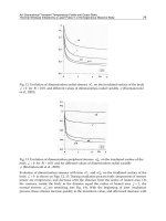
(a) Schematics representing bending of the stamp during NIL, which results from different sinking
velocities due to the stamp geometry. (b) Optical micrograph of a grating with 400 nm period
imprinted in PMMA. The structural area of 5 mm × 3 mm is located in the center of a full 4 inch
Si wafer. Profilometric height measurement of a cross-section schematically represented in nm
indicates large resist thickness variations near and within the grating due to the wafer bending.
360
420
360
250
300
310
390
Fast
Slow
Slow
310
250
300
420
390
Large
unstructured
surrounding
Large
structured
area
Large
unstructured
surrounding
(a) (b)
DK532X_book.fm Page 98 Friday, November 10, 2006 3:31 PM
© 2007 by Taylor & Francis Group, LLC
Nanoimprinting Technology for Biological Applications 99
the surrounding area, the polymer thickness stays almost constant. The
different sinking velocities result in a local bending of the stamp during NIL,
during the removal of the residual layer in order to ensure complete transfer
of the structures.
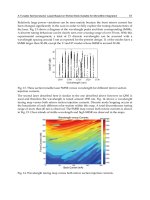
The actual mechanism of the squeeze flow of a resist into a stamp cavity
is a complex function of imprinting conditions [11,15,19,20]. The initial stage
of the filling could occur in two different ways: the first beginning from the
borders of the stamp cavity and the second filling from the center. Different
initial filling behaviors were experimentally observed. A simulation study
by Jeong et al. clearly indicates that the capillary force, surface tension, and
width of the stamp groove are important factors determining the initial filling
behavior (Figure 4.4) [19]. For large width, the resist initially fills the stamp
cavity from the borders. When the feature width decreases, the deformation
mode also changes. The simulation correctly predicts the flow behavior
reported by Heyderman et al., which was attributed to capillary-driven flow
rather than shear-thinning phenomena [15].
FIGURE 4.4
(a) The geometry of computation domain, and (b) simulated free surface shapes during the
initial state of NIL for different geometries (W = 10 µm, 1 µm, and 100 nm), surface energy,
and embossing velocities. (Courtesy of J H. Jeong, J H. Jeong, Y S. Choi, Y J Shin, J J. Lee,
K T. Park, E S. Lee, and S R. Lee, Fibers and Polymers 3, 3 (2002) 113.)
Resist
Stamp cavity
Embossing
velocity, V
e
W
Stamp
Substrate
(a)
s = 29.7 mN/m
V
e
= 0
at t = 2.44 sec
s = 0
V
e
= 7.31 nm/s
at t = 2.46 sec
s = 29.7 mN/m
V
e
= 7.31 nm/s
at t = 2.41 sec
W = 10 µm
W = 1 µm
W = 100 nm
s = 29.7 mN/m
V
e
= 0
at t = 0.276 sec
s = 0
V
e
= 10.2 nm/s
at t = 0.236 sec
s = 29.7 mN/m
V
e
= 10.2 nm/s
at t = 0.220 sec
s = 29.7 mN/m
V
e
= 0
at t = 0.0288 sec
s = 29.7 mN/m
V
e
= 10.6 nm/s
at t = 0.0275 sec
s = 0
V
e
= 10.6 nm/s
at t = 0.0259 sec
(b)
DK532X_book.fm Page 99 Friday, November 10, 2006 3:31 PM
producing a residual layer with inhomogeneous thickness distribution (Fig-
ure 4.3). Thus, care must be taken with the amount of resist thinned down
© 2007 by Taylor & Francis Group, LLC
104 Bio-MEMS: Technologies and Applications
sensitivity of assays and to enable studies of fluid transport and molecular
behavior at extremely small dimensions [4,5,40,42]. For this purpose, NIL is
a ready method of defining fluidic channels of the micro- and nanoscales at
low cost. Apart from the formation of channels, there are also other aspects
that need to be considered in designing a nanofluidic device, which include
modifying surface functionalities, sealing of the channels, integration with
other microstructures for feeding and detection of fluids, and so forth.
Modifying surface functionalities in the channels is an essential process in
the realization of functioning micro- and nanofluidic devices. For example, in
order to transport biological molecules within a device, it is necessary to confine
their motion along the channel while the molecule should not be adsorbed by
the channel walls or escape from the channels. In this regard, it is sometimes
necessary to have surface functionalities of the channel walls be different from
those on the channel track. Recently, Cheng et al. developed an effective method
of achieving highly efficient guiding of microtubules transported by kinesin
motors that are immobilized within polymer nanotracks created by NIL [41].
The nanoscale protein tracks constrained by polymer barriers made of a
cyclized perfluoropolymer called CYTOP, prevent the gliding microtubules
from swaying and compel them to approach the track edge at glancing angles,
thus restraining them from moving out of the track. Furthermore, the surface
of the CYTOP barriers are chemically modified to have protein-nonadhesive
properties, which effectively prevent microtubules from either climbing up the
barriers or randomly gliding over the top surface of the barriers.
The fabrication of nanofluidic channels is completed by sealing of the
channel using either rigid or soft materials following NIL to produce high-
resolution nanoscale templates. Despite the relative ease of constructing
nanoscale structures via NIL, the sealing of these structures into functional
nanofluidic devices presents great technical challenges. Taking advantage of
the filling behavior of resist during NIL, Guo et al. developed a simple
method of fabricating enclosed nanofluidic channels [10,40]. If a very thin
polymer layer is used during imprinting, the displaced polymer will not be
able to fill the trenches on the mold completely, therefore creating enclosed
controlled to give a predictable channel width and height. The channel width
is determined by the feature sizes on the channel template used for imprint-
ing. The channel height can be controlled by the depth of the template and
the initial thickness of the polymer layer, as well as by adjusting the ratio of
the ridge width to the trench width on the channel template. One of the
biological applications has been illustrated by stretching genomic DNA in
such nanochannel arrays. Over 90% stretching has been observed in
nanochannels with a cross-section size of approximately 120 nm × 75 nm
as well as the dynamic behavior of DNA molecules in confined geometries.
Nanofluidics reduces the size of fluidic systems dramatically. However, it
is not simply a matter of shrinking components. Another challenge is how
to integrate those nanostructures with other components of micro- or even
DK532X_book.fm Page 104 Friday, November 10, 2006 3:31 PM
nanochannel features (Figure 4.6). The fabrication process can also be well
(Figure 4.7). Thus, nanofluidic channels could be used for studying the static
© 2007 by Taylor & Francis Group, LLC
108 Bio-MEMS: Technologies and Applications
which has become a major challenge for electronic, optoelectronic, biological,
and sensing applications [1–4,51,52]. In general, local modification of surface
chemistry requires the process sequence of nanofabrication via a suitable
patterning method, followed by selective localization of a molecule using
chemistry known for its immobilization.
A simple method of fabricating chemical nanopatterns using NIL is based
on its pattern transfer ability, which has shown sub–10 nm resolution in the
generation of metal lift-off [59]. The process is schematically shown in Figure
4.9a. After the window opening by O
2
RIE, selective chemical modification
of the substrate surface is achieved by deposition of a molecule with certain
functionalities that need to be imposed on the local substrate surface areas.
Finally, the chemical patterning will be completed by lift-off of the remaining
resist using a solvent. The chemical modification can be performed either in
the gas phase or by dipping in the solution. Figure 4.9b shows atomic/lateral
force microscopy (AFM/LFM) images for chemical patterns with a mixture
of fluorinated mono- and trichlorosilanes fabricated by the method described
in Figure 4.9a. Periodic contrasts in topology, as well as friction force between
areas of the silane molecules and the background, are clearly distinguished
in the images. The smallest width for SiO
2
lines was 15 nm. The results clearly
demonstrate the capability of NIL as a tool for the local modification of
chemical functionalities on a surface in an unprecedented lateral resolution
by combining with an appropriate surface chemistry.
FIGURE 4.9
(a) Process schemes of fabricating chemical patterns via NIL and (b) AFM/LFM images for
chemically patterned surfaces modified with a mixture of fluorinated mono- and trichlorosi-
lanes.
Stamp
(a) (b)
PMMA
Deposit
Deposit
HP = 25 nm
100 nm
100 nm
0 nm
0 nm
3 nm 0.15 V
0.15 V
0 V
0 V
3 nm
Fluorinated silane
– 35 nm
Fluorinated silane
– 50 nm
SiO
2
–20 nm
SiO
–15 nm
Surface
modification
Lift-off
RIE etching
Demolding
Imprinting
SiO
2
Si or SiO
2
AFM LFM
HP = 35.5 nm
DK532X_book.fm Page 108 Friday, November 10, 2006 3:31 PM
© 2007 by Taylor & Francis Group, LLC
110 Bio-MEMS: Technologies and Applications
polyelectrolyte copolymers, such as cationic poly(L-lysine)-graft-poly(ethyl-
ene glycol) (PLL-g-PEG) on transparent negatively charged niobium oxide
(Nb
2
O
5
)–coated glass slides. After achieving chemical contrast of PLL-g-
PEG/PEG-biotin and Nb
2
O
5
, the Nb
2
O
5
areas were rendered nonfouling by
spontaneous adsorption of the nonfunctionalized PLL-g-PEG from an aque-
ous solution to inhibit nonspecific protein adsorption in the background
(Figure 4.10a). In the final step, fluorescence-labeled alexa-488-conjugated
streptavidin was adsorbed onto the biotin functionalized patterned surfaces.
Scanning near-field optical microscopy (SNOM) was used to image the pro-
tein adsorption onto the 100 nm PLL-g-PEG/PEG-biotin stripes. Even
though the fluorescent-labeled lines appear broader than the actual line
width of the PLL-g-PEG/PEG-biotin stripes due to the resolution limit of
SNOM of approximately 100 nm, the regular line pattern of 400 nm–period-
icity is clearly recognized, verifying selective adsorption of the streptavidin.
The second approach developed by Guo et al. consists of nanoscale pat-
terning via NIL and a fluoropolymer surface passivation [10,40]. In contrast
to prevent nonspecific adsorption of biological molecules was done using
CHF
3
RIE immediately after the window-opening step. In their study, pat-
terns of selectively passivated Si surfaces are created using NIL, O
2
RIE, and
deposition of a passivating (CF
x
)
n
polymer, which prevents nonspecific
adsorption of the biological molecules in the unpatterned regions. The tem-
plate surface was then processed with a sequence of chemical modification
steps, and an aminosilane monolayer, biotin, streptavidin, and ultimately a
FIGURE 4.10
(a) AFM image for the chemical pattern of PLL-g-PEG/PEG-biotin after backfilling with PLL-
g-PEG. (b) Scanning near-field optical microscope (SNOM) image after adsorption of a fluores-
cent labeled protein, alexa-488-streptavidin on the chemical pattern shown in (a). (Modified
from D. Falconnet, D. Pasqui, S. Park, R. Eckert, H. Schift, J. Gobrecht, R. Barbucci, and Marcus
Textor, Nano Letters 4, 19 (2004) 1909.)
AFM
5 nm
0 nm
400 nm
400 nm
PLL-g-PEG
PLL-g-PEG/PEG-biotin
SNOM
Adsorption of
alexa-488-
streptavidin
PLL-g-PEG/PEG-biotin
alexa-4BB-streptavidin
PLL-g-PEG
DK532X_book.fm Page 110 Friday, November 10, 2006 3:31 PM
to the chemical patterning process shown in Figure 4.9a, the local passivation
© 2007 by Taylor & Francis Group, LLC
Nanoimprinting Technology for Biological Applications 113
[14] H. Schift, L .J. Heyderman, M. Auf der Maur, and J. Gobrecht, Pattern formation
in hot embossing of thin polymer films, Nanotechnology 12 (2001) 173.
[15] L. J. Heyderman, H. Schift, C. David, J. Gobrecht, and T. Schweizer, Flow
behaviour of thin polymer films used for hot embossing lithography, Micro-
electron. Eng. 54 (2000) 229.
[16] H. Schift, C. David, M. Gabriel, J. Gobrecht, L.J. Heyderman, W. Kaiser, S.
Köppel, and L. Scandella, Nanoreplication in polymers using hot embossing
and injection molding, Microelectron. Eng. 53 (2000) 171.
[17] H. Schift, C. David, J. Gobrecht, A. D’Amore, D. Simoneta, W. Kaiser, and M.
Gabriel, Quantitative analysis of the molding of nanostructures, J. Vac. Sci.
Technol. B 18 (2000) 3564.
[18] H C. Scheer and H. Schulz, A contribution to the flow behaviour of thin
polymer films during hot embossing lithography, Microelectron. Eng. 56 (2001)
311–332.
[19] J H. Jeong, Y S. Choi, Y J Shin, J J. Lee, K T. Park, E S. Lee, and S R. Lee,
Flow behavior at the embossing stage of nanoimprint lithography, Fibers and
Polymers 3, 3 (2002) 113.
[20] H.D. Rowland and W.P. King, Polymer deformation and filling modes during
microembossing, J. Micromech. Microeng. 14 (2004) 1625.
[21] K. Pfeiffer, G. Bleidiessel, G. Gruetzner, H. Schulz, T. Hoffmann, H C. Scheer,
C. M. Sotomayor Torres, and J. Ahopelto, Suitability of new polymer materials
with adjustable glass temperature for nano-imprinting, Microelectron. Eng. 46
(1999) 431.
[22] K. Pfeiffer, F. Reuther, M. Fink, G. Gruetzner, P. Carlberg, I. Maximov, L.
Montelius, J. Seekamp, S. Zankovych, C. M. Sotomayor-Torres, H. Schulz, and
H C. Scheer, A comparison of thermally and photochemically cross-linked
polymers for nanoimprinting, Microelectron. Eng. 67–68 (2003) 266.
[23] W. Zhang and S.Y. Chou, Multilevel nanoimprint lithography with submicron
alignment over 4 in. Si wafers, Appl. Phys. Lett. 79, 6 (2001) 845.
[24] A. Lebib, Y. Chen, J. Bourneix, F. Carcenac, E. Cambril, L. Couraud, and H.
Launois, Nanoimprint lithography for a large area pattern replication, Micro-
electron. Eng. 46 (1999) 431.
[25] K. Pfeiffer, M. Fink, G. Ahrens, G. Gruetzner, F. Reuther, J. Seekamp, S. Zank-
ovych, C. M. Sotomayor Torres, I. Maximov, M. Beck, M. Graczyk, L. Montelius,
H. Schulz, H. -C. Scheer, and F. Steingrueber, Polymer stamps for nanoimprint-
ing, Microelectron. Eng. 61–62 (2002) 393.
[26] S. Park, H. Schift, H.H. Solak, and J. Gobrecht, Stamps for nanoimprint lithog-
raphy by EUV interference lithography, J. of Vac. Sci. Technol. B 22, 6 (2004) 3246.
[27] Z. Yu and S.Y. Chou, Triangular profile imprint molds in nanograting fabrica-
tion, Nano Letters 4, 2 (2004) 341.
[28] Z. Yu, L. Chen, W. Wu, H. Ge, and S.Y. Chou, Fabrication of nanoscale gratings
with reduced line edge roughness using nanoimprint lithography, J. Vac. Sci.
Technol. B 21, 5 (2003) 2089.
[29] S. Park, H. Schift, C. Padeste, B. Schnyder, R. Kötz, and J. Gobrecht, Anti-
adhesive layers on nickel stamps for nanoimprint lithography, Microelectron.
Eng. 73–74 (2004) 196.
[30] S. Park, H. Schift, C. Padeste, A. Scheybal, T. Jung, B. Schnyder, R. Kötz, and
J. Gobrecht, Improved anti-adhesive coating for nanoimprint lithography by
co-evaporation of tri- and monochlorosilanes, Mat. Res. Soc. Proc. EXS-2
(2004) 37.
DK532X_book.fm Page 113 Friday, November 10, 2006 3:31 PM
© 2007 by Taylor & Francis Group, LLC