Photodiodes Communications Bio Sensings Measurements and High Energy Part 4 doc
Bạn đang xem bản rút gọn của tài liệu. Xem và tải ngay bản đầy đủ của tài liệu tại đây (1.09 MB, 20 trang )
The Optimum Link Design Using a Linear PIN-PD for WiMAX RoF Communication
51
coaxial cable and the 10km optical fiber between the VSG and VSA. The third one used the
coaxial cable, the 10km optical fiber, and the parabolic grid antennas between the VSG and
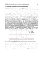
the VSA. Figure2.5 shows the experimental data and the theoretical data that are calculated
with the equation (2.1). The experimental data of the received power coincided within 2dB
with the theoretical data.
Fig. 2.5. The received powers were measured with modulation powers of driving the DFB
laser for three different types of system configurations. The solid lines showed the
experimental data and the dashed lines showed theoretical data calculated with the
equation
2.4 RCE in RoF of WiMAX
It was considered that the RCE was determined with the received power and the noise
power ratio when the RoF system was configured with linear characteristic components and
the optimized modulation condition that were not influenced by the PMD and PML.
However it is not realistic to completely eliminate the influence by the PMD and PML in the
actual link system. A compensation factor to the received power has to be taken into
account. Hence, the RCE is expressed using a compensation factor and a noise power as
NR
RCE P A P
(2.2)
where, RCE [dB] is the Relative Constellation Error,
R
P [dBm] is the received power, A is
the compensation factor to the received power, and
N
P is the system noise power. In the
calculation the following parameters are used; A= 0.857 and
N
P =-84.3[dBm].
Photodiodes – Communications, Bio-Sensings, Measurements and High-Energy Physics
52
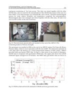
The RCE was also measured with those three different system configurations. Figure 2.6
shows the experimental data and the theoretical data that are calculated with the equation
(2.2). In the full components configuration system, the RCE experimental data coincide
within 2 dB with the theoretical data. In the coaxial cable components configuration system,
there was a little discrepancy between the experimental and the theoretical data in the lower
RCE. This was due to that the noise power
N
P used in the calculation was derived for the
full components configuration system. It is obvious that the noise power
N
P has to be used
for unique value for each system configuration. But, by using the noise power
N
P of full
components configuration system, the RCE for the different type of the configuration
system can be estimated. This means that the equation (2.1) and (2.2) are valid for any
components configuration of the RoF system for the WiMAX, and are useful for the RoF
system design and analysis.
Fig. 2.6. The RCE were measured with modulation powers of DFB laser for the different
type of system configurations. The solid lines show the experimental data and the dashed
lines show theoretical data calculated with the equation (2.2).
It is possible to minimize the influence of the PMD and the PML by optimizing the carrier
frequency, the fiber length, the type of the fiber, and the type of the coupler. The burst signal
received power of the RoF of WiMAX was determined by the transmitter modulation, when
the RoF link was configured with optically and electrically linear characteristic components.
Since the RCE in the RoF of the WiMAX was related to the burst signal receiver power, the
RCE was expressed in the linear relation with the burst signal received power. The
experimental data and theoretical data mostly coincided within 2dB for the received power
and the RCE.
The Optimum Link Design Using a Linear PIN-PD for WiMAX RoF Communication
53
3. E/O and O/E in WiMAX RoF
The WiMAX is a new standard for high-speed wireless communication that covers wider
area than that of WLAN. For the field service, many access points are required, and it is
important to design them with small size, low power consumption, and high reliability.
Therefore, the complicated RF modem and signal processing functions are transferred from
the access points to a central control office [3]. To extend the distance between the access
points and the central office, the use of RoF is suitable for the WiMAX. There have been
several studies of the lower cost and the high performance solutions for the RoF of WLAN
[4]. The use of Vertical Cavity Surface Emitting Laser (VCSEL) or Fabry-Perot Laser Diode
(FP-LD) was suggested for a low cost solution, and Mach-Zender Modulator (MZM) and
Electro-Absorption Modulator (EAM) were used to achieve a high performance. However,
there have been few studies for the RoF of WiMAX. A cost effective design was investigated
for the E/O and the O/E that satisfy both the low cost and the high performance for the
WiMAX RoF.
3.1 WiMAX RoF access points
In the WiMAX field service, a lot of access points are required, as shown in Fig.3.1.
Therefore, it is important to design the access points with low power consumption, small
mechanical size, high reliability, long distance installation, and low cost. A solution to those
requirements is that the signal processing function such as the frequency up-down
converter, modulator and demodulator, and A/D converter shall be transferred to the
central office, and the access point is modified to the remote antenna unit (RAU) that has a
transceiver antenna, and E/O and O/E converters [5], [6]. The RoF link enables installation
of the access units in a long distance from the central office.
Fig. 3.1. The WiMAX RoF links connect between the central office and the access points.
Photodiodes – Communications, Bio-Sensings, Measurements and High-Energy Physics
54
3.2 Input Impedance adjustments in E/O converters
Two different types of 1310nm InGaAsP lasers of DFB and FP type lasers were used for the
E/O converter. The package of the laser was Transmitter Optical Sub-Assembly (TOSA) that
was a low cost design with a receptacle optical interface. We investigated if the electrical
and optical conversion efficiency was increased with adjusting the input impedance of the
E/O converter. The input impedance of the lasers at the 2.4GHz was adjusted on a network
analyzer by changing the R, C, and L elements at the Radio-Frequency (RF) line of the Bias-
Tee. In case of adjusting the input impedance to 50Ω, the input impedance was moved from
the initial value of 15-j55Ωto the matching point of 49.5-j33Ω by adding 33Ω resistor, 1nH
inductor, and 4.7pF capacitor to the RF line, as shown in Fig.3.2. In case of adjusting the
input impedance to a low value, the impedance was moved from the initial value of 15-
j50Ωto the low value point of 7-j2.07Ω by adding 22nH inductor to the RF line, as shown in
Fig.3.3. In case of FP-LD, in addition to the inductor, a capacitor was used. After the input
impedance adjustment, the E/O conversion efficiency was measured by a light-wave optical
component analyzer (N4373A+N5230A, Agilent). The low-impedance input laser
modulation showed about 5dB higher E/O conversion efficiency than that of 50Ω input
impedance laser, as shown in Table 3.1. Although the length of the RF coaxial cable was
about 50cm, the electrical reflectance did not affect the E/O conversion efficiency.
Fig. 3.2. TOSA type E/O with Bias-Tee, Bias-Tee circuit for 50Ω input- impedance adjusting ,
Input-impedance adjusting with R,C, and L elements, on a network analyzer.
The Optimum Link Design Using a Linear PIN-PD for WiMAX RoF Communication
55
Fig. 3.3. TOSA type E/O with Bias-Tee, Bias-Tee circuit for input- low impedance adjusting ,
Input-impedance adjusting with L element, on a network analyzer.
Table 3.1. E/O input-impedance adjusting and E/O conversion
The E/O conversion of the laser is able to be derived by the following equation;
50
20 lo
g
()[]
EO SE
in
dB
Z
(3.1)
where,
EO
is the electrical and optical conversion efficiency [dB],
SE
is the laser slope
efficiency [W/A], and
in
Z is the laser input impedance [Ω] .
According to the equation (3.1), the electrical optical conversion efficiency of the low input
impedance laser is higher than that of the 50Ω input impedance laser by 7 to 8.5dB, but the
measured value showed a difference of 3.7 to 5dB. The difference might be due to the
electrical reflectance between the laser and the signal generator. The theoretical calculation
and the experimental result showed the low input impedance laser had higher electrical and
optical conversion efficiency.
Photodiodes – Communications, Bio-Sensings, Measurements and High-Energy Physics
56
3.3 O/E converters configured with PIN-PD and various type amplifiers
There are several different types of InGaAs PIN-PDs, front-ends, and packages for the
candidate of the O/E converters, since the high speed digital communication and
multichannel wideband analog communication have developed the high performance PIN-
PDs, the low impedance front-end, the transimpedance front end, and the reliable
packages[8]. Four different types of the O/Es were configured as a cost effective solution of
the design of the O/E converter, A linear PIN-PD designed for analog modulation, and a
high speed PIN-PD designed for the 2.5Gb/s or 10Gb/s speeds were used. Two different
types of packages of the coaxial pigtailed type and the ROSA type were used. Four different
types of the pre-amplifiers designed with multi stages GaAs Enhancement-Mode
Pseudomorphic High Electron Mobility Transistor (EP-HEMT), or with a combination of
GaAs Trans-impedance Amplifier (TIA) and the EP-HEMT amplifier, were configured. The
reason of the use of the EP-HEMT was to achieve low voltage single power supply, low
noise figure, and high power gain. Table3.2 shows the O/E converters that were fabricated
with various parameters of those components to investigate the optimum performance. The
O/E conversion gain of those O/E converters was measured with the light-wave optical
component analyzer (N4373A+N5230A, Agilent). The 2.5Gb/s digital PIN-PD has a 2kΩ
trans-impedance amplifier in the ROSA package, and is followed by a 15dB gain EP-HEMT
amplifier. The total gain measured with the optical component analyzer was 33.8 dB. The
10Gb/s digital PIN-PD has a 1.5kΩ TIA and a low gain pre-amplifier in the coplanar type
package. The total gain measured with the optical component analyzer was 35 dB. The pre-
amplifier used in the 10Gb/s O/E converter has a gain control function.
Table 3.2. O/E converters with PIN-PD and EP-HEMT Amplifiers
The Optimum Link Design Using a Linear PIN-PD for WiMAX RoF Communication
57
The O/E conversion of the laser is able to be derived by the following equation;
20
1
20 lo
g
(10)[]
50
v
G
OE R t
SZ dB
(3.2)
where,
OE
is Optical and Electrical conversion efficiency [dB], 50 is the measurement
equipment input impedance [Ω],
R
S is responsivity of the PIN-PD,
t
Z is the trans-
impedance [Ω] ,
v
G is the pre-amplifier gain [dB].
3.4 RCE measurements at 30 to 40km WiMAX RoF transmission
In the experiments of the evaluation of the E/O and O/E converters, a downlink WiMAX
signal (IEEE 802.16) with 10MHz BW and with multi burst sub-frames of BPSK, QPSK,
16QAM, and 64QAM, was used at a 2.4GHz carrier frequency. The received signal error was
evaluated by using the RCE that indicated average-error for all the sub-frames modulations.
The WiMAX signal was generated by a VSG ( E4438C, Agilent), and was converted to
optical signal by the E/O converters. After the transmission over a SMF, the optical signal
was converted to electrical signal by the O/E converter. The received signal was analysed
by a VSA ( 89600S, Agilent).
The WiMAX downlink standard of the IEEE802.16 requires a value of -30dB for the RCE as
the maximum value at the access point. The RCE measured for the FP-LD, the DFB-LD, the
low and 50Ω input impedances are shown in Fig.3.4. The SMF length was 30km. The DFB-
LD showed the lowest RCE. This is due to the lower relative intensity noise (RIN, about -
155dB/Hz) of the DFB-LD. The low input-impedance DFB-LD showed lower RCE, this was
due to the high electrical and optical conversion efficiency (see Table.3.1).
Fig. 3.4. RCE measured with FP-LD, DFB-LD, low input-impedance, and 50Ω input-
impedance.
Photodiodes – Communications, Bio-Sensings, Measurements and High-Energy Physics
58
Figure3.5 shows the RCE measured for the three different types of the O/Es. The PIN1-
AMP1 was configured with a linear PIN-PD and an EP-HEMT amplifier (17dB gain at
2GHz). The intrinsic layer of the linear PIN-PD was optimized for the low distortion
modulation. The PIN2-AMP2 was a ROSA that was configured with a PIN-PD and a 2kΩ
GaAs TIA designed for 2.5Gb/s digital transmission. The PIN1-AMP4 was configured with
a linear PIN-PD and a high gain EP-HEMT amplifier (44.8dB gain at 2GHz). Each amplifier
gain was confirmed on the measurements with the light-wave optical component analyzer
(N4373A+N5230A, Agilent) and with the received electrical power measured at the VSA.
The linear type analog PIN-PD of the type of PIN1 showed lower RCE than that of the
digital PIN-PD of the type of PIN2 that was followed by relatively high gain TIA, as shown
in Fig.3.5. The low gain PIN1-AMP1 showed lower RCE than that of the PIN2-AMP2. This
is due to the low distortion conversion in the analog PIN-PD.
Fig. 3.5. RCE measured with analog PIN-PD (PIN1-AMP1) and 2.5Gb/s digital PIN-PD
(PIN2-AMP2).
In the WiMAX RoF link, the use of the linear PIN-PD is strictly important to reduce the RCE.
In general, the linear PIN-PD is achieved by a specific design of the structure [9]. The
diameter of the window layer has to be determined by the received power, the focused size
of the input light beam, and the capacitance. When increasing the diameter, the linearity in
the higher optical power level is improved, but the cut-off frequency becomes lower. The
length of the intrinsic layer determines the higher optical power level. The longer length is
suitable, if the electric field is high, the distribution of the impurities is uniform, and the
carrier density is low. The maximum length of the intrinsic layer is around the inverse of the
optical absorption coefficient. The longer length of the intrinsic layer may cause the long
The Optimum Link Design Using a Linear PIN-PD for WiMAX RoF Communication
59
carrier drift time, a low electric field, and lack of the uniformity. Since the PIN-PD designed
for the high speed digital application has a small diameter and a short intrinsic layer, the
optical linearity is not sufficient for the WiMAX communication.
Table. 3.3. RCE measured with analog PIN-PD (PIN1-AMP1) and 2.5Gb/s digital PIN-PD
(PIN2-AMP2).
4. Conclusions
It is possible to minimize the influence of the PMD and the PML by optimizing the carrier
frequency, the fiber length, the type of the fiber, and the type of the coupler. The burst signal
received power of the RoF of WiMAX was determined by the transmitter modulation, when
the RoF link was configured with optically and electrically linear characteristic components.
Therefore it is strictly important to use the linear PIN-PD for the optical receiver. Since the
RCE in the RoF of the WiMAX was related to the burst signal receiver power, the RCE was
expressed in the linear relation with the burst signal received power. The experimental data
and theoretical data mostly coincided within 2dB for the received power and the RCE.
An optimum design of the E/O and the O/E converters for a cost effective access point was
carried out. Four different types of the E/O converters and four different types of the O/E
converters were evaluated with the RCE on a WiMAX RoF link using a 2.5GHz carrier
signal. At the transmission link between 30 and 40km, to satisfy the lower cost and the RCE
less than -30dB, it is suitable to use the 1310nm DFB-LD with a pigtailed package, the lower
input impedance than 10Ω, and an EP-HEMT multistage amplifier with the gain larger than
40dB. In this case, it is also strictly important to use the linear PIN-PD that was originally
designed for analog transmission.
5. References
[1] Prasanna A. Gamage, et.al.(2008). Power Optimized Optical Links for Hybride Access
Networks. Opto-Electronics and Communications Conference (OECC) and the
Australian Conference on Optical Fibre Technology (ACOFT), Australia, July 7-10,
2008
[2] Koyu Chinen (2008). RCE Measurements in ROF of IEEE802.16 – 2004 (WiMAX) with
Structurally Optimized DFB Lasers. The 8 th International Conference on Wireless
and Optical Communications (WOC2008), Canada, May 26-28, 2008, pp.48-52
Photodiodes – Communications, Bio-Sensings, Measurements and High-Energy Physics
60
[3] H.Al-Raweshidy and S. Komaki (2002). Radio over Fiber Technologies for Mobile
Communications Networks (Artech House, 2002) Chap.4 .
[4] Andrey Kobyakov. et.al.(2006). 802.11a/g WLAN Radio Transmission at 1.3um over 1.1
km Multi-mode and >30km Standard Single-mode Fiber Using InP VCSEL. In
Proc. ECOC 2006, Cannes, France, 2006, Paper Tu1.6.1.
[5] Mohammad Shaifur Rahman, Jung Hyun Lee, Youngil Park, and Ki-Doo Kim (2009).
Radio over Fiber as a Cost Effective Technology for Transmission of WiMAX
Signals. World Academy of Science, Engineering and Technology, vol. 56, pp.424-428,
(2009)
[6] Chien-Hung Yeh, Chi-WaiChow, Yen-Liang Liu, Sz-Kai Wen, Shi-Yang Chen, Chorng-
Ren Sheu, Min-Chien Tseng, Jiunn-Liang Lin, Dar-Zu Hsu, and Sien Chi (2010).
Theory and Technology for Standard WiMAX Over Fiber in High Speed Train
Systems. Journal of Lightwave Technology, vol.28, No.16, Aug. 15, pp.2327-2336,
(2010)
[7] Charles H.Cox, III (2004). Analog Optical Links , Cambridge University Press
[8] Eduard Sackinger(2005). Broadband Circuits for Optical Fiber Communications, John
Wiley & Sons, Inc.
[9] Avigdor Brillant (2008). Digital and Analog Fiber Optic Communications for CATV and
FTTx Applications, SPIE and John Wiley &Sons, Inc.
4
Single Photon Detection Using Frequency
Up-Conversion with Pulse Pumping
Lijun Ma, Oliver Slattery and Xiao Tang
Information Technology laboratory, National Institute of Standards and Technology
United States of America
1. Introduction
In any quantum communication system, such as a quantum key distribution (QKD) system,
data rates are mainly limited by the system clock rate and the various link losses. While the
transmission clock rate is limited by the temporal resolution of the single-photon detectors,
losses in a fiber-based quantum communication system can be minimized by operating in
the near infrared range (NIR), at 1310 nm or 1550 nm. Commercially available InGaAs-based
avalanche photo-diodes (APDs) can be operated as single-photon detectors in this
wavelength range [Hadfield, 2009]. Due to the severe after-pulsing, InGaAs APDs are
typically used in a gated mode and this can limit their application in high-speed quantum
communications systems. Superconducting single-photon detectors (SSPDs) can work in the
NIR wavelength range with good performance [Gol’tsman et al. 2001; Hadfield, 2009].
However, SSPDs require cryogenic temperatures, and are not widely available on the
commercial market at present. In addition, InGaAs/InP based photomultiplier tubes (PMT)
can operate in the NIR range, but its performance is limited by very low detection efficiency
(1 % at 1600 nm) and large timing jitter (1.5 ns) [Hamamatsu, 2005]. Microchannel plates
(MCP) are micro-capillary electron multipliers coated with an electron-emissive material
and multiply photon-excited electrons from a photon cathode [Wiza, 1979]. MCPs usually
have faster rise times and lower timing jitter than is achievable with PMTs. InGaAs MCPs
can work in the NIR range. These MCPs, but are limited by low detection efficiency (~1 %)
[Martin, J. & Hink P. 2003].
On the other hand, silicon based avalanche photo-diodes (Si APDs) are compact, relatively
inexpensive, and can be operated at ambient temperatures with high detection efficiency
and low noise in the visible or near-visible range. Unfortunately they do not work at
wavelengths longer than 1000 nm. For those wavelengths, an up-conversion technique has
been developed that uses sum-frequency generation (SFG) in a non-linear optical medium to
convert the signal photons to a higher frequency (shorter wavelength) in the visible or near
visible range. The up-converted photons can then be detected by a Si APD. Up-conversion
detectors use commercially available components and devices, and are a practical solution
for many applications in quantum communications. To date, several groups have
successfully developed highly efficient up-conversion single-photon detectors in the near-
infrared range using periodically poled lithium niobate (PPLN) waveguides [Diamanti et
al., 2005; Langrock et al., 2005; Thew et al., 2006; Tanzilli et al., 2005; Xu et al., 2007;] and
bulk crystals [Vandevender & Kwiat, 2004].
Photodiodes – Communications, Bio-Sensings, Measurements and High-Energy
62
Traditionally, an up-conversion single photon detector uses continuous wave (CW)
pumping at a single wavelength. For a quantum communication system, a synchronized
clock signal can be obtained from classical channels. Therefore, the up-conversion detector
can be operated in pulsed pump mode using the synchronized clock signal. Up-conversion
detectors with a pulsed pump can provide extra advantages that CW pumped detectors do
not offer. For example, because the dark count rate in an up-conversion detector is
dependent on the pump power, pulsed pump can significantly reduce the noise while
keeping the same conversion efficiency. Furthermore, in the CW pump mode, the temporal
resolution is determined by the timing jitter of the Si APD used in the detection system. The
jitter-limited temporal resolution becomes a bottleneck as the transmission rate increases in
a quantum communications system. An up-conversion single-photon detector using
multiple spectrally and temporally distinct pulse pumps can support transmission rates
significantly higher than the jitter-limited transmission rate of a traditional Si APD detector.
In this chapter, we will describe in detail an up-conversion detector using a pulsed pump
and its applications in noise reduction and transmission rate increase in quantum
communication systems. This detector was developed at the National Institute of Standards
and Technology.
2. Up-conversion detector with one wavelength pulsed pumping
2.1 Detector configuration
The configuration of an up-conversion detector with a single wavelength pulsed pump is
shown in Fig. 1.
A 1550 nm CW laser provides the pump seed. The CW seed light is modulated to an optical
pulse train by a Lithium Niobate-based electro-optical modulator (EO modulator). In many
quantum information systems, the photons arrive with a synchronized classical signal. One
can use the synchronized signal to modulate the pump seed resulting in the up-conversion
detector operating a pulsed pump mode. This feature is similar to an optical gate, which is
very useful for noise reduction or high speed gating in a communications system.
The modulated pump seed is then amplified by an erbium-doped fiber amplifier (EDFA).
Two 1310/1550 wavelength division multiplexer (WDM) couplers with a 25 dB extinction
ratio are used to suppress noise around 1310 nm at the output of the EDFA. The amplified
pump light is then combined with a weak (single photon) signal in the 1310 nm range by
another WDM coupler and the combined pump and signal are then coupled into the
PPLN waveguides. The input polarization state of both the signal and the pump are
adjusted by the polarization controllers, PC1 and PC2 respectively, before entering the
coupler. The longer the waveguide length, the lower the pump power needed to reach the
maximum conversion efficiency. The PPLN waveguide for the up-conversion detector is
5-cm long, the longest length possible using current manufacturing techniques. The input
of the PPLN waveguide is fiber coupled, and the output is coupled into free-space
through a 710 nm anti-reflection (AR) coating on the face of the waveguide. The output
light of PPLN waveguide consists of a 710 nm (SFG) up-converted weak light signal,
residual 1550 nm pump light and its second harmonic generation (SHG) light at 775 nm.
These beams are separated by two dispersive prisms and the 710 nm photons are detected
by a Si APD. An iris and a 20 nm band-pass filter are used to reduce other noise, such as
external light leaked into the system.
Single Photon Detection Using Frequency Up-Conversion with Pulse Pumping
63
Fig. 1. Schematic diagram of an up-conversion detector with a pulsed pump. EOM: Electric-
optic modulator; EDFA: Erbium-doped fiber amplifier; WDM: Wavelength-division
multiplexing coupler; PC: Polarization controller; PPLN: Periodically-poled LiNbO3
waveguides; IF: Interference filter. Solid line: Optical fiber; Dash line: Free space optical
transmission.
2.2 Noise reduction in quantum communication systems
The noise, or dark counts, of a single photon detector is one of its important performance
parameters: a higher dark count rate can cause more errors in the quantum information
system and degrade the system’s fidelity.
In an up-conversion single photon detector, the total dark counts originate from the intrinsic
dark counts of the Si APD and the noise from the frequency conversion process inside the
crystal. The intrinsic dark count rate is very low, and is usually negligible in comparison to
the noise due to the frequency conversion process. It is widely believed that the noise which
arises in the frequency conversion process stems from the spontaneous Raman scattering
(SRS) [Diamanti et al., 2005; Langrock et al., 2005; Thew et al., 2006; Tanzilli et al., 2005; Xu et
al., 2007; Vandevender & Kwiat, 2004] and spontaneous parametric down conversion
(SPDC) [Pelc et al, 2010] generated in the waveguide by the strong pump. If these SRS
photons or SPDC photons are generated at wavelengths within the signal band they can be
up-converted to the detection wavelength, generating noise or ‘dark’ counts. In our
experiment, we have shown that a pump using a longer wavelength than the signal avoids
the SPDC photons leaving only the noise from the anti-Stokes photons of SRS.
The significance of the Raman scattering component can be estimated by first neglecting the
SFG, loss, and pump depletion, and then solving the photon number for a given Stokes
mode
s
N using the differential equation of the Raman scattering [Smith, 1972] in a known
length PPLN waveguide. The solution is given by
s
1
gL
Ne
, (1)
where the Raman gain, g, is given by
/
e
ff
PA
and
L
represents the length. The quantity
is the gain factor and the pump power,
P , divided by the effective area,
e
ff
A
, gives the
pump intensity.
In the above configuration, the 240-nm wavelength spacing between the pump (1550 nm)
and the signal (1310 nm) is much larger than the peak Raman shift frequency of PPLN.
Therefore,
Photodiodes – Communications, Bio-Sensings, Measurements and High-Energy
64
1,
gL
e
g
L
(2)
and the stimulated Raman scattering inside the PPLN is also negligible since a relatively low
pump power is used. Therefore, we can assume that most of the Stokes photons are induced
by the spontaneous Raman scattering inside the PPLN and this assumption enables a simple
solution for the dark count.
The internal conversion efficiency (
C
) in the PPLN waveguide is a function of pump
power, and is determined by the following equation [Diamanti et al., 2005; Langrock et al.,
2005; Thew et al., 2006; Tanzilli et al., 2005; Xu et al., 2007; Vandevender & Kwiat, 2004]:
2
0
sin / ,
Ceff
PkPAL
(3)
where
0
is the peak conversion efficiency.
0
is dependent on the quality of the PPLN
waveguide and can reach 1 in a waveguide with high poling quality. The pump intensity is
the ratio of the power,
P
,to the effective area,
e
ff
A .
PPLN
L
is the PPLN waveguide length.
k is a constant and determined by
2
1/2
2
(),
speff
sp
d
k
nnc
(4)
where
s
and
p
are the signal and pump wavelengths;
s
n and
p
n
are the refractive index
of lithium niobate for the signal and pump wavelengths.
e
ff
d represents the effective
nonlinear coefficient and c is the speed of light.
Using the above assumptions in Eq. (1), one can get a differential equation for the Stokes
photon:
//
se
ff
dN dz
g
PA
with
z being a distance inside the PPLN waveguide from
the input surface. A generated Stokes photon will be up-converted to the detection
wavelength and induce a dark count. Consequently, by further applying the conversion
efficiency of the PPLN, Eq. (3-4), we can write the dark count rate, DCR, as a function of
pump power:
PPLN
2
APD T
0
eff
APD T PPLN
eff
sin /
sin 2 /
1 ,
2
2/
L
Raman eff
eff
eff
P
DCR P L z k P A dz
A
kP A L
PL
A
kP A L
(5)
where
T
is the overall transmission efficiency and
APD
is the detection efficiency of the Si
APD. The linear term of the pump power,
P ,in the integral describes the generation of
Stokes photons via the spontaneous Raman scattering and the sinusoidal term describes the
up-conversion of the Stokes photons generated at
z
contributing to a dark count at the
PPLN output (
z
= L ). In the above derivation, we also neglected the optical loss in the
PPLN waveguide. This assumption is justified by the fact that low waveguide loss is
achieved with current manufacturing techniques and nearly 100 % internal conversion
efficiency has been reported.
Single Photon Detection Using Frequency Up-Conversion with Pulse Pumping
65
From the above analyses, one can see the conversion efficiency and noise both are
dependent on the pump power. In a quantum communication system, each time bin is
usually much longer than the optical pulse, because the single photon detectors have large
timing jitter. When the pump pulse width is larger than the optical signal width, the
photons can be converted at the highest efficiency. By turning off the pump after the signal
pulse the dark counts rate can be reduced. When the pump is off, Si-APDs and counting
board still operate, so the counts triggered by the signal photons delayed by the detector’s
jitter can still be recorded. In that case, we can reduce the noise while the efficiency is not
affected.
We have experimentally demonstrated the up-conversion detector with a pulsed pump. The
conversion efficiency as the function of pump power is shown in Fig. 2. The detection
efficiency measured here is from a 625 MHz synchronized signal with 600 ps (FWHM)
pump pulses. The optical pulse is pumped with the same synchronized signal but has a
shorter (300 ps FWHM) pulse width. The detector operating in pulsed pump mode can
reach the maximum conversion efficiency with a lower average pump power, which helps
to reduce noise. The optimal pump powers (average) are 38 mW and 78 mW, for the pulsed
and CW pump modes respectively.
0
5
10
15
20
25
30
35
0 20406080
Pump Power (mW)
Detection efficiency (%)
Fig. 2. The detection efficiency as a function of pump power. Two cases are studied: CW
pump (triangle) and pulsed pump (square).
As shown in the Fig. 3, the pulsed pump generates more dark counts than the CW pump for
a given average power since the peak power of the pulsed pump is higher than the average
power. However, the pulsed pump needs less average power than the CW pump to achieve
a given detection efficiency. Therefore, the pulse pump can achieve a given detection
efficiency with less dark counts in comparison to the CW pump. For example, the maximum
detection efficiency is reached when using the pulsed pump at 38 mW and the dark count
rate is 2400 c/s. For the CW pump, a power of 78 mW is needed to achieve the maximum
detection efficiency, which incurs a dark count rate of 3100 c/s. Consequently, a pulsed
pump needs lower average power and effectively reduces the dark count rate compared to a
CW pump.
Photodiodes – Communications, Bio-Sensings, Measurements and High-Energy
66
0
1000
2000
3000
4000
5000
0 20406080
Pump Power (mW)
Dark Counts Rate (Hz)
Fig. 3. The dark count rate as a function of average pump power at the PPLN input. Two
cases are studied: CW pump (triangle) and pulsed pump (square).
To demonstrate the performance of the above up-conversion detector with pulsed pumping,
we integrated them into one of our QKD system [Xu et al., 2007]. The quantum keys are
encoded by photons in the quantum channel at 1310 nm using the B92 protocol [Bennett,
1992], as shown in Fig. 4. The QKD system uses a custom printed circuit board with a field-
programmable gate array (FPGA) [Mink et al. 2006; Mink et al. 2009] to generate a random
stream of quantum data for the photons and to transmit and receive the classical data. The
classical data is carried by the optical signal in the classical channel at 1550 nm. To
polarization-encode the quantum channel with the random quantum data, we first
modulate a 1310-nm CW light into a 625 MHz pulse train, which is evenly split into two
polarization channels. Each pulse train is further modulated by one of two complementary
625 Mbit/s quantum channel data streams. The two quantum channels are combined by a
45-degree polarization-maintaining combiner and attenuated to a mean photon number of
0.1 per bit, and then multiplexed with the classical channel and sent to a standard single-
mode fiber. At Bob, another WDM is used to demultiplex the quantum and classical
channels. The quantum channel is polarization-decoded and detected using the up-
conversion single-photon detectors, and the detection events are recorded to generate raw
keys. Bob’s board informs Alice of the location of the detection events via the classical
channel. After reconciliation and error correction, Alice and Bob obtain a common version of
shared secret key bits, which are further used to encode and decode information for secure
communication between Alice and Bob.
The system performance is shown in Fig. 5. During our measurements, the pump power
was fixed at 40 mW. The sifted-key rate is 2.5 Mbit/s for a back-to-back connection, 1
Mbit/s at 10 km, and 60 Kbit/s at 50 km. The quantum bit error rate (QBER) is
approximately 3% for the back-to-back configuration, remains below 4% up to 20 km, and
reaches 8% at 50 km. The finite extinction ratio of the modulator and the system timing jitter
induce a background QBER of approximately 2.5% and the rest is from dark counts
generated by both the pump light and the classical channel. We also calculated the
theoretical sifted-key rate and QBER and they agree well with the measured results.
Single Photon Detection Using Frequency Up-Conversion with Pulse Pumping
67
TRCV
PCI
PCI
FPGA
Ser/Des
Ser/Des
FPGA
Ser/Des
Ser/Des
Bob PCAlice PC
TRCV
A L I C E
B O B
Fiber
EOM0
LD
EOM1
WDM
Alice
WDM
Bob
EOM1
PMC
45
Clock
Quantum
Data
Classical
Data
VOA
Coupler
Up-Conversion
Detector
CR
Coupler
Clock
Classical
Data
Quantum
Data
Pol.
Fig. 4. The B92 polarization coding QKD system. LD: Laser diode; EOM: Electric-optic
modulator (LiNbO3); PC: Polarization controller; PMC-45º: Polarization maintaining
combiner that combines two light signals that are separated by 45 degrees; VOA: Variable
optical attenuator; WDM: Wavelength-division multiplexer; SMF: Standard single-mode
fiber; TRCV: Optical transceiver; CR: Clock recovery module; FPGA: Custom printed circuit
board controlled by a field-programmable gate array; PCI: PCI connection; Dotted line:
Electric cable; Solid line: Optical fiber.
Although the pump power is fixed near the optimal value for maximum up-conversion
efficiency, the QBER remains small until the distance reaches close to 20 km due to the low
dark count rate caused by the 1550 nm up-conversion detector. This QKD system can generate
secure keys in real time for one-time-pad encryption and decryption of a continuous 200
Kbit/s video transmission stream over 10 km fiber. The system performance demonstrates that
the up-conversion detectors with pulse pumping are suitable for the fiber-based polarization-
encoding QKD system, realizing high speed secured data transmission.
0.01
0.1
1
10
0 1020304050
Distance (km)
Sifted Key Rate (Mbit/s)
0
1
2
3
4
5
6
7
8
9
QBER (%)
Measured SKR
Calcuated SKR
QBER
Fig. 5. The system performance of the B92 polarization-based QKD system using pulsed
pump up-conversion detectors.
Photodiodes – Communications, Bio-Sensings, Measurements and High-Energy
68
3. Up-conversion detector with multiple wavelength pulse pumping
3.1 The scheme and detector configuration
In many recent quantum communication systems, the photon sources can generate and
temporally encode data at rates significantly higher than what single-photon detectors can
resolve. For example, commercially available mode-locked lasers or optical modulators can
generate sub-10 ps optical pulses, and broadband SPDC sources can readily prepare optical
states of photon pairs with sub-100 fs correlation time. On the other hand, current high-
resolution single-photon detectors exhibit a FWHM temporal resolution of the order of 50
ps. In a quantum communication system, insufficient temporal resolution in the detector can
cause inter-symbol interference (ISI), i.e., a detection signal can be recorded at a time slot
adjacent to the intended one, and this can induce a significant error rate. The transmission
rate is therefore limited by the temporal resolution of the single-photon detectors. As a
figure of merit, a single-photon signal can be received with an acceptable error rate when
the transmission period is equal to or larger than the full width at 1% of the maximum
(FW1%M) of the single-photon detector’s response histogram [Restelli et al. 2009]. For most
types of Si APDs the FW1%M is significantly larger than the commonly cited FWHM. At the
peak of a typical Si APD’s response histogram, where the FWHM is measured, the profile is
approximately Gaussian. However, at lower part of the detector’s response curve, the
response histogram profile deviates significantly from Gaussian, often exhibiting a long
exponential tail, which dramatically increases the FW1%M of the device. A typical
commercially-available Si APD has a FWHM of about 350 ps, but a FW1%M of about 1100
ps that limits the transmission rate to less than 1 GHz for a quantum communication system
using an up-conversion detector equipped with this type of Si APD.
Fig. 6. Schematic diagram of up-conversion single-photon detection with multi-wavelength
optical sampling. A sequence of n spectrally and temporally distinct pump pulses are used
to sub-divide the minimum resolvable time bin,
det
, of conventional Si APDs, increasing the
temporal resolution of the overall system by a factor of n. The incident single-photon signal
is combined with the sequence of pump pulses with a wavelength division multiplexer
(WDM). Detection events from each of the n Si APDs are time-tagged with time-correlated
single-photon counting (TCSPC).
Single Photon Detection Using Frequency Up-Conversion with Pulse Pumping
69
To increase the temporal resolution of an up-conversion detection system beyond that of its
constituent Si APDs, a sequence of spectrally and temporally distinct pump pulses can be
used to sub-divide the minimum resolvable time period
det
. This application of optical
sampling is illustrated in Fig. 6, where
n pump pulses with different wavelengths are used
to sample the incident single-photon signal in intervals of duration
det
/n. To ensure
optimum detection efficiency, each pump pulse is wider than the single-photon signal
pulses. The repetition rate for each particular wavelength of the pump is
1/
det
. When a
signal photon enters and co-propagates with one of the strong pump pulses in a quasi-phase
matched sum-frequency device, such as PPLN, it can be up-converted to the visible range.
The specific wavelength of the up-converted photon is determined by the wavelength of the
pump pulse with which it interacted. A subsequent dispersive element such as a grating can
separate the up-converted signal photons and distribute them to an array of Si APDs. Each
Si APD in the array therefore corresponds to a particular pump wavelength, and, by
extension, a particular arrival time period of duration
det
/n. In such a configuration the
sampling period for each Si APD is
det
, allowing it to accurately resolve the signal without
ambiguity due to the detector’s temporal response. With this approach, the detection system
is able to resolve the single-photon signal in a period as small as
det
/n, representing an
increase in temporal resolution by a factor of
n.
The experimental configuration of an up-conversion detector with a multiple wavelength
pulse pump is shown in Fig. 7. A pattern generator drives the pulse-carving systems for the
two up-conversion pump sources at 1549.2 nm and 1550.0 nm. Each pump source has a
period of 1.25 ns. Before the pump and the signal are combined the pulses from the first
pump are aligned with the odd signal pulses, and the pulses in the second pump are aligned
Fig. 7. Experimental setup. LD: Laser Diode, EOM: Electric-optic Modulator; EDFA: Erbium-
doped fiber amplifier; WDM: Wavelength-division multiplexing coupler; PC: Polarization
controller; PPLN: Periodically-poled LiNbO3 waveguides; OL, Objective Lens; HG,
Holographic Grating. TCSPC: time-correlated single photon counting;
Photodiodes – Communications, Bio-Sensings, Measurements and High-Energy
70
with the even signal pulses by adjusting the delays in the pattern generator, as shown in Fig.
8. The pump-pulse duration used in the experiment is 400 ps, which is wider than the 220 ps
signal pulse and chosen to provide higher conversion efficiency [Xu et al., 2007]. The two
pump beams are combined by a 1x2 coupler and then amplified by a 1-Watt EDFA. At the
output of the EDFA, two 1310/1550 WDM couplers are used in series, giving a 50-dB
extinction ratio in total, to suppress noise around 1310 nm. The amplified pump light is then
combined with the 1310-nm signal by another WDM coupler, and the combined pump and
signal are coupled into the up-conversion medium. Up-conversion takes place in a 1-cm
PPLN waveguide that has a fiber-coupled input and a free-space output. When mixed with
the slightly different pump wavelengths in the PPLN waveguide, the 1310 nm signal
photons are up-converted to output photons at 710.0 nm and 709.8 nm. The output beam is
filtered to remove noise and excess pump light and then diffracted by a holographic grating.
After a 3-m long path the 710.0 nm and 709.8 nm photons are sufficiently separated that they
can be directed onto two Si APDs. In this system an adjustable iris placed in front of the Si
APD, in conjunction with the holographic grating, act as a 0.4-nm band-pass filter, which
greatly reduces the dark count rate. The detected signals are then counted by a time-
correlated single photon counting system.
Fig. 8. Timing diagram of the signal, pump 1 and pump 2 used in the multi-wavelength
optical sampling single-photon detection system.
In this experiment we use a 1-cm long PPLN waveguide. A shorter waveguide provides a
broader spectral bandwidth, which is necessary to cover the spectral separation of the two
output photons. In the previously described work, we have demonstrated high single-
photon up-conversion efficiency with a longer 5-cm PPLN waveguide, but we find that the
quasi-phase matched bandwidth for such a waveguide is too narrow for the current
approach. The transfer function response of a finite-length uniform quasi-phase matching
grating is [Fejer et al. 1992]:
2
() sinc( /2),
SFG pump signal
IkII kL (6)