MEMS and Microstructures in Aerospace Applications - Robert Osiander et al (Eds) Part 2 pot
Bạn đang xem bản rút gọn của tài liệu. Xem và tải ngay bản đầy đủ của tài liệu tại đây (1.34 MB, 18 trang )
balance. One potential solution to this design problem is to employ the MEMS
micromachined shutters to create, in essence, a variable emittance coating (VEC).
Such a VEC yields changes in the emissivity of a thermal control surface to allow
the radiative heat transfer rate to be modulated as needed for various spacecraft
operational scenarios. In the case of the ST5 flight experiment, the JHU/APL
MEMS thermal shutters will be exercised to perform adaptive thermal control of
the spacecraft by varying the effective emissivity of the radiator surface.
2.2.2 JWST MICROSHUTTER ARRAY
NASA’s James Webb Space Telescope (JWST) is a large (6.5-m primary mirror
diameter) infrared-optimized space telescope scheduled for launch in 2011. JWST
is designed to study the earliest galaxies and some of the first stars formed after the
Big Bang. When operational, this infrared observatory will take the place of the
Hubble Space Telescope and will be used to study the universe at the important but
previously unobserved epoch of galaxy formation. Over the past several years,
scientists and technologists at NASA GSFC have developed a large format
MEMS-based microshutter array that is ultimately intended for use in the JWST
near infrared spectrometer (NIRSpec) instrument. It will serve as a programmable
field selector for the spectrometer and the complete microshutter system will be
FIGURE 2.2 The NMP ST5 MEMS thermal louver actuator block with shutter array.
(Source: JHU/APL.)
Osiander / MEMS and microstructures in Aerospace applications DK3181_c002 Final Proof page 18 1.9.2005 11:49am
18 MEMS and Microstructures in Aerospace Applications
© 2006 by Taylor & Francis Group, LLC
composed of four 175 by 384 pixel modules. This device significantly enhances the
capability of the JWST since the microshutters can be selectively configured to
make highly efficient use of nearly the entire NIRSpec detector, obtaining hundreds
of object spectra simultaneously.
Micromachined out of a silicon nitride membrane, this device, as shown in
Figure 2.3 and Figure 2
.4,
consists of a 2-D array of closely packed and independ-
ently selectable shutter elements. This array functions as an adaptive input mask for
the multiobject NIRSpec, providing very high contrast between its open and closed
states. It provides high-transmission efficiency in regions where shutters are com-
manded open and where there is sufficient photon blocking in closed areas. Oper-
ationally, the desired configuration of the array will be established via ground
command, then simultaneous observations of multiple celestial targets can be
obtained.
Some of the key design challenges for the microshutter array include obtaining
the required optical (contrast) performance, individual shutter addressing, actuation,
latching, mechanical interfaces, electronics, reliability, and environment require-
ments. For this particular NIRSpec application, the MEMS microshutter developers
also had to ensure the device would function at the 37 K operating temperature of
the spectrometer as well as meet the demanding low-power dissipation requirement.
Figure 2.5 shows the ability to address or actuate and provide the required
contrast demonstrated on a fully functional 128 by 64 pixel module in 2003 and the
development proceeding the 175 by 384 pixel flight-ready microshutter module that
will be used in the JWST NIRSpec application. This is an outstanding example of
applying MEMS technology to significantly enhance the science return from a
space-based observatory.
FIGURE 2.3 JWST microshutters for the NIRSpec detector. (Source: NASA.)
Osiander / MEMS and microstructures in Aerospace applications DK3181_c002 Final Proof page 19 1.9.2005 11:49am
Vision for Microtechnology Space Missions 19
© 2006 by Taylor & Francis Group, LLC
2.2.4 NMP ST6 INERTIAL STELLAR CAMERA
NASA’s NMP is sponsoring the development of the inertial stellar compass (ISC)
space avionics technology that combines MEMS inertial sensors (gyroscopes)
with a wide field-of-view active pixel sensor (APS) star camera in a compact,
multifunctional package.
6
This technology development and maturation activity is
being performed by the Charles Stark Draper Laboratory (CSDL) for a Space
Technology-6 (ST6) flight validation experiment now scheduled to fly in 2005.
The ISC technology is one of several MEMS technology development activities
being pursued at CSDL
7
and, in particular, is an outgrowth of earlier CSDL research
focused in the areas of MEMS-based guidance, navigation, and control (GN&C)
sensors or actuators
8
and low-power MEMS-based space avionic systems for
space.
9
The ISC, shown in Figure 2.6, is a miniature, low-power, stellar inertial
attitude determination system that provides an accuracy of better than 0.18
(1-Sigma) in three axes while consuming only 3.5 W and is packaged in a 2.5-kg
housing.
10
The ISC MEMS gyro assembly, as shown in Figure 2.7, incorporates CSDL’s
tuning fork gyro (TFG) sensors and mixed signal application specific integrated
Alignment Reference Cube
CGA Housing
Baffle
Lens Assembly
DC - DC
Converter
Camera PWA
DPA PSE PWA
Controller and PSE PWA
DPA Housing
Processor PWA
Lens and Camera Support Assembly
DC - DC Converter
Gyro PWA
FIGURE 2.6 The NMP ST6 inertial stellar camera. (Source: NASA JPL/CALTECH ST6.)
Osiander / MEMS and microstructures in Aerospace applications DK3181_c002 Final Proof page 21 1.9.2005 11:49am
Vision for Microtechnology Space Missions 21
© 2006 by Taylor & Francis Group, LLC
that serves to free up precious spacecraft resources. For example, the mass
savings afforded by using the MEMS-based ISC could be allocated for additional
propellant or, likewise, the power savings could potentially be directly applied to
the mission payload. These are some of the advantages afforded by using MEMS
technology.
2.2.5 MICROTHRUSTERS
Over the past several years MEMS catalytic monopropellant microthruster research
and development has been conducted at NASA’s GSFC.
11
MEMS-based propulsion
systems have the potential to enable missions that require micropropulsive maneu-
vers for formation flying and precision pointing of micro-, nano-, or pico-sized
satellites. Current propulsion technology cannot meet the minimum thrust require-
ments (10–1000 mN) or impulse-bit requirements (1–1000 mNÁsec), or satisfy the
severely limited system mass (<0.1 kg), volume (<1cm
3
), and power constraints
(<1 W). When compared to other proposed micropropulsion concepts, MEMS
catalytic monopropellant thrusters show the promise of the combined advantages
of high specific density, low system power and volume, large range of thrust levels,
repeatable thrust vectors, and simplicity of integration. Overall, this approach offers
an attractive technology solution to provide scalable micro-Newton level micro-
thrusters. This particular MEMS microthruster design utilizes hydrogen peroxide as
the propellant and the targeted thrust level range is between 10 and 500 mN with
impulse bits between 1 and 1000 mNÁ sec and a specific impulse (I
sp
) greater than
110 sec.
A prototype MEMS microthruster hardware has been fabricated as seen in
Figure 2.8, using GSFC’s detector development laboratory (DDL) facilities and
equipment. Individual MEMS fabricated reaction chambers are approximately 3.0
 2.5  2.0 mm. Thrust chambers are etched in a 0.5 mm silicon substrate and the
vapor is deposited with silver using a catalyst mask.
2.2.6 OTHER EXAMPLES OF SPACE MEMS DEVELOPMENTS
The small sampling of space MEMS developments given earlier can be categorized
as some very significant technological steps toward the ultimate goal of routine and
systematic infusion of this technology in future space platforms. Clearly NASA
researchers have identified several areas where MEMS technology will substan-
tially improve the performance and functionality of the future spacecraft. NASA is
currently investing at an increasing rate in a number of different MEMS technology
areas. A review of the NASA Technology Inventory shows that in fiscal year 2003
there were a total of 111 distinct MEMS-based technology development tasks being
funded by NASA. Relative to GFY02 where 77 MEMS-based technology tasks
were cataloged in the NASA Technology Inventory, this is over a 40% increase in
MEMS tasks. It is almost a 90% increase relative to GFY01 where 59 MEMS R&D
tasks were identified. The MEMS technologies included in the NASA inventory
are:
Osiander / MEMS and microstructures in Aerospace applications DK3181_c002 Final Proof page 23 1.9.2005 11:49am
Vision for Microtechnology Space Missions 23
© 2006 by Taylor & Francis Group, LLC
.
Microheat-sinks for microsat thermal control applications
.
Tunable Fabry–Perot etalon optical filters for remote sensing applications
5
.
Two-axis fine-pointing micromirrors for intersatellite optical communica-
tions applications.
16
2.3 POTENTIAL SPACE APPLICATIONS FOR MEMS TECHNOLOGY
It should be apparent that the near-term benefit of MEMS technology is that
it allows developers to rescale existing macrosystems down to the microsystem
level. However, beyond simply shrinking today’s devices, the true beauty of
MEMS technology derives from the system redefinition freedom it provides to
designers, leading to the invention of entirely new classes of highly integrated
microsystems.
It is envisioned that MEMS technology will serve as both an ‘‘enhancing’’ and
an ‘‘enabling’’ technology for many future science and exploration missions. En-
abling technologies are those that provide the presently unavailable capabilities
necessary for a mission’s implementation and are vital to both intermediate and
long-term missions. Enhancing technologies typically provide significant mission
performance improvements, mitigations of critical mission risks, and significant
increases in mission critical resources (e.g., cost, power, and mass).
MEMS technology should have a profound and far-reaching impact on many of
NASA’s future space platforms. Satellites in low-Earth orbit, deep-space interplan-
etary probes, planetary rovers, advanced space telescopes, lunar orbiters, and lunar
landers could all likely benefit in some way from the infusion of versatile MEMS
technology. Many see the future potential for highly integrated spacecraft architec-
tures where boundaries between traditional, individual bus and payload subsystems
are at a minimum blurred, or in some extreme applications, nonexistent with the
infusion of multifunctional MEMS-based microsystems.
NASA’s GSFC has pursued several efforts not only to increase the general
awareness of MEMS within the space community but also to spur along specific
mission-unique infusions of MEMS technology where appropriate. Over the past
several years the space mission architects at the GSFC’s Integrated Mission Design
Center (IMDC), where collaborative end-to-end mission conceptual design studies
are performed, have evaluated the feasibility of using MEMS technology in a
number of mission applications. As part of this MEMS technology ‘‘push’’ effort,
many MEMS-based devices emerging from research laboratories have been added
to the IMDC’s component database used by the mission conceptual design team.
The IMDC is also a rich source of future mission requirements and constraints data
that can be used to derive functional and performance specifications to guide
MEMS technology developments. Careful analysis of these data will help to
identify those missions where infusing a specific MEMS technology will have a
significant impact, or conversely, identifying where an investment in a broadly app-
licable ‘‘crosscutting’’ MEMS technology will yield benefits to multiple missions.
The remainder of this section covers some high-priority space mission applica-
tion areas where MEMS technology infusion would appear to be beneficial.
Osiander / MEMS and microstructures in Aerospace applications DK3181_c002 Final Proof page 25 1.9.2005 11:50am
Vision for Microtechnology Space Missions 25
© 2006 by Taylor & Francis Group, LLC
2.3.1 INVENTORY OF MEMS-BASED SPACECRAFT COMPONENTS
It is expected that MEMS technology will offer NASA mission designers very
attractive alternatives for challenging applications where power, mass, and volume
constraints preclude the use of the traditional components. MEMS technologies will
enable miniaturized, low-mass, low-power, modular versions of many of the current
inventory of traditional spacecraft components.
2.3.2 AFFORDABLE MICROSATELLITES
A strong driver for MEMS technology infusion comes from the desire of some
space mission architects to implement affordable constellations of multiple micro-
satellites. These constellations, of perhaps as many as 30–100 satellites, could be
deployed either in loosely controlled formations to perform spatial or temporal
space environment measurements, or in tightly controlled formations to synthesize
distributed sparse aperture arrays for planet finding.
A critical aspect to implementing these multisatellite constellations in today’s
cost-capped fiscal environment will be the application of new technologies that
reduce the per unit spacecraft cost while maintaining the necessary functional
performance. The influence of technology in reducing spacecraft costs evaluated
by NASA
17
through analysis of historical trend data leads us to the conclusion that,
on average, the use of technologies that reduce spacecraft power will reduce
spacecraft mass and cost. Clearly a large part of solving the affordable microsatel-
lite problem will involve economies of scale. Identifying exactly those technologies
that have the highest likelihood of lowering spacecraft cost is still in progress.
However, a case can be made that employing MEMS technology, perhaps in
tandem with the ultra-low power electronics
18
technology being developed by
NASA and its partners, will be a significant step toward producing multiple micro-
satellite units in a more affordable way.
It should also be pointed out that another equally important aspect to lowering
spacecraft costs will be developing architectures that call for the use of standard-
off-the-shelf and modular MEMS-based microsystems. Also, there will be a need
to fundamentally shift away from the current ‘‘hands on’’ labor-intensive limited-
production spacecraft manufacturing paradigm toward a high-volume, more ‘‘hands
off’’ production model. This would most likely require implementing new cost-
effective manufacturing methodologies where such things as parts screening, sub-
system testing, spacecraft-level integration and testing, and documentation costs are
reduced.
One can anticipate the ‘‘Factory of the Future,’’ which produces microsatellites
that are highly integrated with MEMS-based microsubsystems, composed of mini-
aturized electronics, devices and mechanisms, for communications, power, and
attitude control, extendable booms and antennas, microthrusters, and a broad
range of microsensor instrumentation. The multimission utility of having a broadly
capable nano- or microspacecraft has not been overlooked by NASA’s mission
Osiander / MEMS and microstructures in Aerospace applications DK3181_c002 Final Proof page 26 1.9.2005 11:50am
26 MEMS and Microstructures in Aerospace Applications
© 2006 by Taylor & Francis Group, LLC
architects. New capabilities such as this will generate new concepts of space
operations to perform existing missions and, of greater import, to enable entirely
new types of missions.
Furthermore, because the per unit spacecraft cost has been made low enough
through the infusion of MEMS technology, the concept of flying ‘‘replaceable’’
microsatellites is both technically and economically feasible. In such a mission
concept, the requirements for redundancy or reliability will be satisfied at the
spacecraft level, not at the subsystem level where it typically occurs in today’s
design paradigm. In other words, MEMS-based technology, together with appro-
priate new approaches to lower spacecraft-level integration, test and launch costs,
could conceivably make it economical to simply perform an on-orbit spacecraft
replacement of a failed spacecraft. This capability opens the door to create new
operational concepts and mission scenarios.
2.3.3 SCIENCE SENSORS AND INSTRUMENTATION
As described in Chapter 7 of this book, the research topic of MEMS-based science
sensors and instruments is an incredibly rich one. Scientists and MEMS technolo-
gists are collaborating to first envision and then rapidly develop highly integrated,
miniaturized, low-mass and power-efficient sensors for both science and explor-
ation missions. The extreme reductions in sensor mass and power attainable via
MEMS technology will make it possible to fly multiple high-performance instru-
mentation suites on microsatellites, nanosatellites, planetary landers, and autono-
mous rovers, entry probes, and interplanetary platforms. The ability to integrate
miniaturized sensors into lunar or planetary In Situ Resource Utilization (ISRU)
systems and/or robotic arms, manipulators, and tools (i.e., a drill bit) will have high
payoff on future exploration missions. Detectors for sensing electromagnetic fields
and particles critical to several future science investigations of solar terrestrial
interactions are being developed in a MEMS format. Sensor technologies using
micromachined optical components, such as microshutters and micromirrors for
advanced space telescopes and spectrometers, are also coming of age. One exciting
research area is the design and development of adaptive optics devices made up of
either very dense arrays of MEMS micromirrors or membrane mirrors to perform
wavefront aberration correction functions in future space observatories. These
technologies have the potential to replace the very expensive and massive high-
precision optical mirrors traditionally employed in large space telescopes. Several
other MEMS-based sensing systems are either being actively developed or are
in the early stages of innovative design. Examples of these include, but are not
limited to, micromachined mass spectrometers (including MEMS microvalves) for
chemical analysis, microbolometers for infrared spectrometry, and entire labora-
tory-on-a-chip device concepts. One can also envision MEMS-based environmental
and state-of-health monitoring sensors being embedded into the structures of
future space transportation vehicles and habitats on the lunar (or eventually on a
planetary) surface as described in the following section on exploration applications
for MEMS.
Osiander / MEMS and microstructures in Aerospace applications DK3181_c002 Final Proof page 27 1.9.2005 11:50am
Vision for Microtechnology Space Missions 27
© 2006 by Taylor & Francis Group, LLC
2.3.4 EXPLORATION APPLICATIONS
There are a vast number of potential application areas for MEMS technology within
the context of the U.S. Vision for Space Exploration (VSE). We explore some of
those here.
In the integrated vehicle health management (IVHM) arena, emphasis will be
placed upon developing fault detection, diagnosis, prognostics, information fusion,
degradation management capabilities for a variety of space exploration vehicles and
platforms. Embedded MEMS technology could certainly play a significant role in
implementing automated spacecraft IVHM systems and the associated crew emer-
gency response advisory systems.
Developing future ISRU systems will dictate the need for automated systems to
collect lunar regolith for use in the production of consumables. Innovative ISRU
systems that minimize mass, power, and volume will be part of future power system
and vehicle refueling stations on the lunar surface and planetary surfaces. These
stations will require new techniques to produce oxygen and hydrogen from lunar
regolith, and further, new systems to produce propellants and other consumables
from the Mars atmosphere will need to be developed.
MEMS technology should also play a role in the development of the space and
surface environmental monitoring systems that will support exploration. Clearly the
observation, knowledge, and prediction of the space, lunar, and planetary environ-
ments will be important for exploration. MEMS could also be exploited in the
development of environmental monitoring systems for lunar and planetary habitats.
This too would be a very suitable area for MEMS technology infusion.
2.3.5 SPACE PARTICLES OR MORPHING ENTITIES
Significant technological changes will blossom in the next few years as the multiple
developments of MEMS, NEMS, micromachining, and biochemical technologies
create a powerful confluence. If the space community at large is properly prepared
and equipped, the opportunity to design, develop, and fly revolutionary, ultra-
integrated mechanical, thermal, chemical, fluidic, and biologic microsystems can
be captured. Building these type of systems is not feasible using conventional space
platform engineering approaches and methods.
Some space visionaries are so enthused by this huge ‘‘blue sky’’ potential as to
blaze completely new design paths over the next 15–25 years. They envision the
creation of such fundamentally new mission ideas as MEMS-based ‘‘spaceborne
sensor particles’’ or autonomously morphing space entities that would resemble
today’s state-of-the-art space platforms as closely as the currently ubiquitous PCs
resemble the slide rules used by an earlier generation of scientists and engineers.
These MEMS-enabled ‘‘spaceborne sensor particles’’ could be used to make very
dense in situ science observations and measurements. One can even envision these
‘‘spaceborne sensor particles’’ breaking the access-to-space bottleneck — which
significantly limits the scope of what we can do in space — by being able to take
advantage of novel space launch systems innovations such as electromagnetic or
Osiander / MEMS and microstructures in Aerospace applications DK3181_c002 Final Proof page 28 1.9.2005 11:50am
28 MEMS and Microstructures in Aerospace Applications
© 2006 by Taylor & Francis Group, LLC
light-gas cannon launchers where perhaps thousands of these devices could be
dispensed at once.
2.4 CHALLENGES AND FUTURE NEEDS
In this section, it will be stressed that while some significant advancements are
being made to develop and infuse MEMS technology into space mission applica-
tions, there is much more progress to be made. There are still many challenges,
barriers, and issues (not all technical or technological) yet to be dealt with to fully
exploit the potential of MEMS in space. The following is a brief summary of some
of the key considerations and hurdles to be faced.
2.4.1 CHALLENGES
History tells us that the infusion of new technological capabilities into space
missions will significantly lag behind that of the commercial or the industrial sector.
Space program managers and other decision makers are typically very cautious
about when and where new technology can be infused into their missions. New
technologies are often perceived to add unnecessary mission risk.
Consequently, MEMS technology developers must acknowledge this barrier to
infusion and strive to overcome it by fostering a two-way understanding and interest
in MEMS capabilities with the mission applications community. This motivates the
need, in addition to continually maturing the Technology Readiness Level (TRL) of
their device or system, to proactively initiate and maintain continuing outreach with
the potential space mission customers to ensure a clear mutual understanding of
MEMS technology benefits, mission requirements and constraints (in particular the
‘‘Mission Assurance’’ space qualification requirements), risk metrics, and potential
infusion opportunities.
2.4.2 FUTURE NEEDS
It is unlikely that the envisioned proliferation of MEMS into future science and
exploration missions will take place without significant future technological
and engineering investments focused on the unique and demanding space applica-
tions arena. Several specific areas where such investments are needed are suggested
here.
Transitioning MEMS microsystems and devices out of the laboratory and into
operational space systems will not necessarily be straightforward. The overwhelm-
ing majority of current MEMS technology developments have been targeted at
terrestrial, nonspace applications. Consequently, many MEMS researchers have
never had to consider the design implications of having to survive and operate in
the space environment. An understanding of the space environment will be a
prerequisite for developing ‘‘flyable’’ MEMS hardware. Those laboratory re-
searchers who are investigating MEMS technology for space applications must
first take the time to study and understand the unique challenges and demanding
Osiander / MEMS and microstructures in Aerospace applications DK3181_c002 Final Proof page 29 1.9.2005 11:50am
Vision for Microtechnology Space Missions 29
© 2006 by Taylor & Francis Group, LLC
requirements imposed by the need to first survive the rigors of the short-term
dynamic space launch environment as well as the long-term on-orbit operating
environments found in various mission regimes. Chapter 4 of this book is intended
to provide just such a broad general background on the space environment and will
be a valuable reference for MEMS technologists. In a complementary effort, the
space system professionals in industry and in government, to whom the demanding
space environmental requirements are routine, must do a much better job of guiding
the MEMS technology community through the hurdles of designing, building, and
qualifying space hardware.
The establishment of much closer working relationships between MEMS tech-
nologists and their counterparts in industry is certainly called for. Significantly
more industry–university collaborations, focused on transitioning MEMS micro-
systems and devices out of the university laboratories, will be needed to spur the
infusion of MEMS technology into future space missions. It is envisioned that these
collaborative teams would target specific space mission applications for MEMS.
Appropriate mission assurance product reliability specifications, large-scale manu-
facturing considerations, together with industry standard mechanical or electrical
interface requirements, would be combined very early in the innovative design
process. In this type of collaboration, university-level pilot production would be
used to evaluate and path find viable approaches for the eventual large volume
industrial production process yielding space-qualified commercial-off-the-shelf
(COTS) MEMS flight hardware.
On a more foundational level, continued investment in expanding and refining
the general MEMS knowledge base will be needed. The focus here should be on
improving our understanding the mechanical and electrical behaviors of existing
MEMS materials (especially in the cryogenic temperature regimes favored by many
space-sensing applications) as well as the development of new exotic MEMS
materials. New techniques for testing materials and methods for performing stand-
ardized reliability assessments will be required. The latter need will certainly drive
the development of improved high-fidelity, and test-validated, analytical software
models. Exploiting the significant recent advances in high-performance computing
and visualization would be a logical first step here.
Another critical need will be the development of new techniques and processes
for precision manufacturing, assembly and integration of silicon-based MEMS
devices with macroscale nonplanar components made from metals, ceramics, plas-
tics, and perhaps more exotic materials. The need for improved tools, methods, and
processes for the design and development of the supporting miniature, low-power
mixed-signal (analog and digital) electronics, which are integral elements of the
MEMS devices, must also be addressed.
The investigation of innovative methods for packing and tightly integrating the
electrical drive signal, data readout, and signal conditioning elements of the MEMS
devices with the mechanical elements should be aggressively pursued. In most
applications, significant device performance improvements, along with dramatic
reductions in corrupting electrical signal noise, can be accomplished by moving the
electronics as physically close as possible to the mechanical elements of the MEMS
Osiander / MEMS and microstructures in Aerospace applications DK3181_c002 Final Proof page 30 1.9.2005 11:50am
30 MEMS and Microstructures in Aerospace Applications
© 2006 by Taylor & Francis Group, LLC
device. This particular area, focused on finding new and better ways to more closely
couple the MEMS electronics and mechanical subelements, can potentially have
high payoffs and should not be overlooked as an important research topic.
Lastly it is important to acknowledge that a unified ‘‘big picture’’ systems
approach to exploiting and infusing MEMS technology in future space missions is
currently lacking and, perhaps worse, nonexistent. While there are clearly many
localized centers of excellence in MEMS microsystem and device technology
development within academia, industry, nonprofit laboratories, and federal govern-
ment facilities, there are few, if any, comparable MEMS systems engineering and
integration centers of excellence. Large numbers of varied MEMS ‘‘standalone’’
devices are being designed and developed, but there is not enough work being done
currently on approaches, methods, tools, and processed to integrate heterogenous
MEMS elements together in a ‘‘system of systems’’ fashion. For example, in the
case of the affordable microsatellite discussed earlier, it is not at all clear how one
would go about effectively and efficiently integrating a MEMS microthruster or a
MEMS microgyro with other MEMS-based satellite elements such as a command
or telemetry system, a power system, or on-board flight processor. We certainly
should not expect to be building future space systems extensively composed of
MEMS microsystems and devices using the integration and interconnection ap-
proaches currently employed. These are typically labor-intensive processes using
interconnection technologies that are both physically cumbersome and resource
(power or mass) consuming. The cost economies and resource benefits of using
miniature mass-produced MEMS-based devices may very well be lost if a signifi-
cant level of ‘‘hands-on’’ manual labor is required to integrate the desired final
payload or platform system. Furthermore, it is quite reasonable to expect that future
space systems will have requirements for MEMS-based payloads and platforms that
are both modular and easily reconfigurable in some ‘‘plug and play’’ fashion. The
work to date on such innovative technology as MEMS harnesses and MEMS
switches begins to address this interconnection or integration need, but significant
work remains to be done in the MEMS flight system engineering arena. In the near
future, to aid in solving the dual scale (macro-to-MEMS) integration problem,
researchers could pursue ways to better exploit newly emerging low power or
radiation hard microelectronics packaging and high-density interconnect technolo-
gies as well as Internet-based wireless command or telemetry interface technology.
Researchers should also evaluate methods to achieve a zero integration time (ZIT)
goal for MEMS flight systems using aspects of today’s plug and play component
technology, which utilizes standard data bus interfaces. Later on, we most likely
will need to identify entirely new architectures and approaches to accomplish the
goal of simply and efficiently interconnecting MEMS microsystems and devices
composed of various types of metals, ceramics, plastics, and exotic materials.
Balancing our collective technological investments between the intellectually
stimulating goal of developing the next best MEMS standalone device in the
laboratory and the real world problem that will be faced by industry of effectively
integrating MEMS-based future space systems is a recommended strategy for
ultimate success. Significant investments are required to develop new space system
Osiander / MEMS and microstructures in Aerospace applications DK3181_c002 Final Proof page 31 1.9.2005 11:50am
Vision for Microtechnology Space Missions 31
© 2006 by Taylor & Francis Group, LLC
engineering approaches to develop adaptive and flexible MEMS flight system
architectures and the supporting new MEMS-scale interconnection hardware or
software building blocks. Likewise the closely associated need to test and validate
these highlyintegrated MEMS ‘‘system of systems’’ configurations prior to launch
will drive the need for adopting (and adapting) the comprehensive, highly autono-
mous built-in test (BIT) functions commonly employed in contemporary nonaero-
space commercial production lines.
Research in this arena could well lead to the establishment of a new MEMS
microsystems engineering discipline. This would be a very positive step in taking
the community down the technological path toward the ultimate goal of routine,
systematic, and straightforward infusion of MEMS technology in future space
missions.
There are several important interrelated common needs that span all the emer-
ging MEMS technology areas. Advanced tools, techniques, and methods for high-
fidelity dynamic modeling and simulation of MEMS microsystems will certainly be
needed, as will be multiple MEMS technology ground testbeds, where system
functionality can be demonstrated and exercised. These testbed environments will
permit the integration of MEMS devices in a flight configuration like hardware-in-
the-loop (HITL) fashion. The findings and the test results generated by the testbeds
will be used to update the MEMS dynamic models. The last common need is for
multiple and frequent opportunities for the on-orbit demonstration and validation of
emerging MEMS-based technologies for space. Much has been accomplished in the
way of technology flight validation under the guidance and sponsorship of such
programs as NASA’s NMP, but many more such opportunities will be required to
propel the process of validating the broad family of MEMS technologies needed to
build new and innovative space systems. The tightly interrelated areas of dynamic
models and simulations, ground testbeds, and on-orbit technology validation mis-
sions will all be essential to fully understand and to safely and effectively infuse the
MEMS into future missions.
2.5 CONCLUSIONS
The success of future science and exploration missions quite possibly will be
dependent on the development, validation, and infusion of MEMS-based micro-
systems that are not only highly integrated, power efficient, and minimally pack-
aged but also flexible and versatile enough to satisfy multimission requirements.
Several MEMS technology developments are already underway for future space
applications. The feasibility of many other MEMS innovations for space is currently
being studied and investigated.
The widespread availability and increasing proliferation of MEMS technology
specifically targeted for space applications will lead future mission architects to
evaluate entirely new design trades and options where MEMS can be effectively
infused to enhance current practices or perhaps enable completely new mission
opportunities. The space community should vigorously embrace the potential
Osiander / MEMS and microstructures in Aerospace applications DK3181_c002 Final Proof page 32 1.9.2005 11:50am
32 MEMS and Microstructures in Aerospace Applications
© 2006 by Taylor & Francis Group, LLC
disruptive technological impact of MEMS on how space systems are designed,
built, and operated. One option is to adopt a technology infusion approach similar to
the one the Defense Advanced Research Projects Agency (DARPA) has pursued for
the development and widespread integration of MEMS-based microsystems to
revolutionize our military’s capabilities on future battlefields. Technologists, re-
searchers, and decision makers interested in developing truly innovative and enab-
ling MEMS-based microsystems that will support the VSE goals of affordability,
reliability, effectiveness, and flexibility would do well to study the DARPA ap-
proach, where multiple high-risk or high-payoff military MEMS technologies are
being pursued to dramatically improve the agility, accuracy, lethality, robustness,
and reliability of warfighter systems.
Transitioning MEMS microsystems and devices out of the laboratory and into
operational space systems will present many challenges. Clearly much has been
accomplished but several critical issues remain to be resolved in order to produce
MEMS microsystems that will satisfy the demanding performance and environ-
mental requirements of space missions. In the spirit of Rear Admiral Grace Murray
Hopper (who is quoted as saying ‘‘If it’s a good idea, go ahead and do it. It’s much
easier to apologize than it is to get permission’’) the community must continue to
innovate with open minds for if we constrain our vision for MEMS in space, an
opportunity may be missed to bend (or even break) current space platform design
and production paradigms.
REFERENCES
1. Osiander, R., S.L. Firebaugh, J.L. Champion, et al., Microelectromechanical devices for
satellite thermal control, IEEE Sensors Journal Microsensors and Microacuators: Tech-
nology and Applications 4(4), pp. 525 (2004).
2. Wesolek, D.M., J.L. Champion, F.A. Hererro, et al., A micro-machined flat plasma
spectrometer (FlaPS), Proceedings of SPIE — The International Society for Optical
Engineering 5344, pp. 89 (2004).
3. Sillon, N. and R. Baptist, Sensors and actuators B (chemical), Proceedings of 11th
International Conference on Solid State Sensors and Actuators Transducers ’01/Euro-
sensors XV, Elsevier, Switzerland, Vol. B83, pp. 129 (2002).
4. Mott, D.B., R. Barclay, A. Bier, et al., Micromachined tunable Fabry–Perot filters for
infrared astronomy, Proceedings of SPIE — The International Society for Optical
Engineering 4841, pp. 578 (2002).
5. George, T., Overview of MEMS/NEMS technology development for space applications
at NASA/JPL, Smart Sensors, Actuators, and MEMS, May 19–21 2003, The International
Society for Optical Engineering, Maspalonas, Gran Canaria, Spain (2003).
6. Brady, T., et al., The inertial stellar compass: a new direction in spacecraft attitude
determination, 16th Annual AIAA/USU Conference on Small Satellites, Logan, UT (2002).
7. Duwel, A. and N. Barbour, MEMS development at Draper lab, Society for Experimental
Mechanics (SEM) Annual Conference (2003).
8. Connelly, J.A., et al., Alignment and performance of the infrared multi-object spectrom-
eter, Cryogenic Optical Systems and Instruments X, Aug 6 2003, The International
Society for Optical Engineering, San Diego, CA (2003).
Osiander / MEMS and microstructures in Aerospace applications DK3181_c002 Final Proof page 33 1.9.2005 11:50am
Vision for Microtechnology Space Missions 33
© 2006 by Taylor & Francis Group, LLC
9. Johnson, W.M. and R.E. Phillips, Space avionics stellar-inertial subsystem, 20th Digital
Avionics Systems Conference Proceedings, Oct 14–18 2001, Institute of Electrical and
Electronics Engineers, Inc., Daytona Beach, FL (2001).
10. Brady, T., et al., A multifunction, low-power attitude determination technology break-
through, AAS G&C Conference, AAS 03–003 (2003).
11. Hitt, D.L., C.M. Zakrzwski, and M.A. Thomas, MEMS-based satellite micropropulsion
via catalyzed hydrogen peroxide decomposition, Smart Materials and Structures 10(6),
pp. 1163–1175 (2001).
12. Caffey, J.R. and P.E. Kladitis, The effects of ionizing radiation on microelectromecha-
nical systems (MEMS) actuators: electrostatic, electrothermal, and bimorph, 17th IEEE
International Conference on Micro Electro Mechanical Systems (MEMS): Maastricht
MEMS 2004 Technical Digest, Jan 25–29 2004, Maastricht, Netherlands, Institute of
Electrical and Electronics Engineers Inc., Piscataway, United States (2004).
13. Hewagama, T., et al., Spectral contrast enhancement techniques for extrasolar planet
imaging, High-Contrast Imaging for Exo-Planet Detection, Aug 23–26 2002. The Inter-
national Society for Optical Engineering, Waikoloa, Hawaii (2002).
14. Siebert, P. G., Petzold, , and J. Muller, Processing of complex microsystems: a micro
mass spectrometer, Proceedings of the SPIE — The International Society for Optical
Engineering 3680, pp. 562 (1999).
15. Bernhard, J.T., et al., Stacked reconfigurable antenna elements for space-based radar
applications, 2001 IEEE Antennas and Propagation Society International Symposium —
Historical Overview of Development of Wireless, Jul 8–13 2001, Institute of Electrical
and Electronics Engineers, Inc., Boston (2001).
16. Graeffe, J., et al., Scanning micromechanical mirror for fine-pointing units of intersa-
tellite optical links, Design, Test, Integration, and Packaging of MEMS/MOEMS, May 9–
11 2000, Paris, Fr, Society of Photo-Optical Instrumentation Engineers, Bellingham,
Washington (2000).
17. Buehler, M.G., et al., Technologies for affordable SEC missions, IEEE Big Sky Confer-
ence (2004).
18. Gambles, J., et al., An ultra-low-power, radiation-tolerant Reed–Solomon Encoder for
space applications. Proceedings of the Custom Integrated Circuits Conference, pp. 631–
634 (2003).
Osiander / MEMS and microstructures in Aerospace applications DK3181_c002 Final Proof page 34 1.9.2005 11:50am
34 MEMS and Microstructures in Aerospace Applications
© 2006 by Taylor & Francis Group, LLC
3
MEMS Fabrication
James J. Allen
CONTENTS
3.1 Introduction 35
3.2 MEMS Fabrication Technologies 36
3.3 LIGA 38
3.4 Bulk Micromachining 40
3.4.1 Wet Etching 41
3.4.2 Plasma Etching 44
3.5 Sacrificial Surface Micromachining 46
3.5.1 SUMMiT V
1
52
3.6 Integration of Electronics and MEMS Technology 55
3.7 Additional MEMS Materials 60
3.7.1 Silicon Carbide 60
3.7.2 Silicon–Germanium 61
3.7.3 Diamond 62
3.7.4 SU-8 62
3.8 Conclusions 62
References 63
3.1 INTRODUCTION
Making devices small has long had engineering, scientific, and esthetic motivations.
John Harrison’s quest
1
to make a small (e.g., hand-sized) chronometer in the 1700s
for nautical navigation was motivated by the desire to have an accurate time-keeping
instrument that was insensitive to temperature, humidity, and motion. A small chron-
ometer could meet these objectives and allow for multiple instruments on a ship for
redundancy and error averaging. The drive toward miniaturization of various mech-
anical and electrical devices advanced over the years, but in the 1950s several key
events occurred that would motivate development at an increased pace.
The development of the transistor
2
in 1952, and a manufacturing method for
a planar silicon transistor
3,4
in 1960 set the stage for development of fabrication
processes to achieve small feature sizes. The drive for microelectronic devices with
smaller and smaller features continues to the present day.
Dr. Richard Feynman presented a seminal talk ‘‘There’s Plenty of Room at the
Bottom’’ on December 29, 1959 at the annual meeting of the American Physical
Osiander / MEMS and microstructures in Aerospace applications DK3181_c003 Final Proof page 35 1.9.2005 8:59pm
35
© 2006 by Taylor & Francis Group, LLC
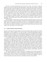
The evaluation of a fabrication process for an application requires the assess-
ment of a number of factors:
.
The process-critical dimension (i.e., the smallest dimension that can be
fabricated)
.
The process precision (i.e., dimensional accuracy or nominal device dimen-
sion)
.
Materials available for fabrication
.
Assembly requirements to produce a functioning device
.
Process scalability (i.e., can large quantities of devices be produced?)
.
Integrability with other fabrication processes (e.g., microelectronics)
A large assortment of MEMS fabrication processes have been developed, but
they may be grouped into three broad categories, which are discussed in further
detail in subsequent sections.
TABLE 3.1
Comparison of the Capabilities of MEMS Fabrication Technologies and
Conventional Machining
Capability LIGA
Bulk
Micromachining
Surface
Micromachining
Conventional
Machining
Feature size ~3 to 5 mm~3to5mm1mm ~10 to 25 mm
Device thickness >1mm >1mm 13mm Very large
Lateral dimension >2mm >2mm 2mm >10 m
Relative tolerance ~10
À2
~10
À2
~10
À1
>10
À3
Materials Electroplated
metals or
injection
molded plastics
Very limited
material suite
Very limited
material suite
Extremely large
material suite
Assembly
requirements
Assembly
required
Assembly
required
Assembled as
fabricated
Assembly
required
Scalability Limited Limited Yes Yes
MicroElectronic
integratability
No Yes for SOI bulk
processes
Yes No
Device geometry Two-dimensional
high aspect
ratio
Two-dimensional
high aspect
ratio
Multi-layer
Two-dimensional
Very flexible
Three-
dimensional
Processing Parallel
processing at
the wafer level
Parallel
processing at
the wafer level
Parallel
processing at
the wafer level
Serial processing
Osiander / MEMS and microstructures in Aerospace applications DK3181_c003 Final Proof page 37 1.9.2005 8:59pm
MEMS Fabrication 37
© 2006 by Taylor & Francis Group, LLC
Surface
Micromachining
Silicon Substrate
Poly Si
Structures formed
by deposition and
etching of sacrificial
and structural thin films.
[100]
Bulk
Micromachining
LIGA
Wet Etch Patterns
Dry Etch Patterns
Mold
Silicon
Substrate
3D structures formed
by wet or dry
etching of silicon
substrate.
3D structures formed
by mold fabrication,
followed by injection
molding or electroplating.
.
Groove
p
++
(B)
Membrane
[111]
Silicon
Substrate
Channels
Holes
54.7Њ
Nozzle
FIGURE 3.1
MEMS fabrication technology categories. (Courtesy: Sandia National
Laboratories.)
Osiander / MEMS and microstructures in Aerospace applications DK3181_c003 Final Proof page 39 1.9.2005 8:59pm
MEMS Fabrication 39
© 2006 by Taylor & Francis Group, LLC
NH
4
F $ NH
3
þ HF (3:2)
Wet-etching methods can also be used on crystalline materials to achieve aniso-
tropic directional etches. For example, a common directional wet etchant for
crystalline silicon is potassium hydroxide (KOH). KOH etches 100 times faster in
the (1 0 0) direction than the (1 1 1) direction. Patterned silicon dioxide can be used
as an etch mask for these types of etches. Very directional etches can be achieved
with these techniques as illustrated in Figure 3.4. Note the angular features (54.7 8)
that can be etched in silicon. Table 3.2 lists some of the common etchants for
crystalline silicon and their selectivity.
If there are no etch stops in a wet-etching process the two options available to
the process engineer are a timed etch or a complete etch through the material.
A timed etch is difficult to control accurately due to the many other variables in the
process such as temperature, chemical agitation, purity, and concentration. If this is
not satisfactory, etch stops can be used to define a boundary for the etch to stop on.
There are several etch-stop methods that can be utilized in wet etching:
.
p
þ
(boron diffusion or implant) etch stop
.
Material-selective etch stop
.
Electrochemical etch stop
Boron-doped silicon has a greatly reduced etch rate in KOH. The use of born-doped
regions, which are either diffused or implanted, has been used either to form
such as silicon nitride, which has a greatly reduced etch rate, can be deposited on a
material to form a membrane on which etching will stop.
An electrochemical etch stop can also be used as shown in Figure 3.6. Silicon
is a material that readily forms a silicon oxide layer, which will impede etching of
the bulk material. The formation of the oxide layer is a reduction–oxidation reaction
that can be impeded by a reverse-biased p–n junction, which prevents the current
φ = 54.7Њ
<111>
<100>
SiO
2
Mask
φ
FIGURE 3.4 Directional etching of crystalline silicon.
Osiander / MEMS and microstructures in Aerospace applications DK3181_c003 Final Proof page 42 1.9.2005 8:59pm
42 MEMS and Microstructures in Aerospace Applications
features or as an etch stop as seen in Figure 3.5. Also, a thin layer of a material
h
© 2006 by Taylor & Francis Group, LLC