Micro Electro Mechanical System Design - James J. Allen Part 6 ppsx
Bạn đang xem bản rút gọn của tài liệu. Xem và tải ngay bản đầy đủ của tài liệu tại đây (1023.85 KB, 30 trang )
Scaling Issues for MEMS 131
One way to make this assessment of electric vs. magnetic fields for actuation
is to consider the energy density of an electric, U
electric
, and a magnetic, U
magnetic
,
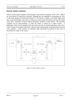
field for a region of space at the appropriate operational condition (Figure 4.11).
Equation 4.25 and Equation 4.26 define the electric and magnetic field density,
respectively, where ε is the permittivity and µ is the permeability of the region
that contains the electric field, E, and the magnetic field, B. For purposes of this
assessment, the free space permittivity, ε
0
= 8.84 × 10
–12
F/M, and the free space
permeability, µ
0
= 1.26 × 10
5
H/M will be used. The maximum value of the
electric field, E, and magnetic field, B, will be limited by the maximum obtainable
operational values.
The maximum obtainable electric field is at the point just before electrostatic
breakdown. This breakdown occurs when the electrons or ions in an electric field
are accelerated to a sufficient energy level so that, when they collide with other
molecules, more ions or electrons are produced, resulting in an avalanche break-
down of the insulating medium; high current flow is produced. For air at standard
temperature and pressure, the electric field at electrostatic breakdown in macro-
scopic scale gaps between electrodes (i.e., > ~10 µm) is E
max
= 3 × 10
6
V/M.
(4.25)
(4.26)
The maximum obtainable magnetic field energy density is limited by the
saturation of the magnetic field flux density in magnetic materials. In materials,
the spin of an electron at the atomic level will produce magnetic effects. In many
FIGURE 4.11 Electric and magnetic fields in a region of space.
V
E
ε - permitivity
µ - permability
B
(a) Electric Field (b) Magnetic Field
U E
electric
=
1
2
2
ε
U
B
magnetic
=
1
2
2
µ
© 2005 by Taylor & Francis Group, LLC
132 Micro Electro Mechanical System Design
materials, these atomic level magnetic effects are canceled out due to their random
orientation. However, in ferromagnetic materials, adjacent atoms have a tendency
to align to form a magnetic domain in which their magnetic effects collectively
add up. Each magnetic domain can be from a few microns to a millimeter in size
[17], depending upon the material and its processing and magnetic history. How-
ever, the domains are randomly oriented and the specimen exhibits no net external
magnetic field. If an external magnetic field is applied, the magnetic domains
will have a tendency to align with the magnetic field.
Figure 4.12 shows a plot of the magnetic flux density, B, vs. the magnetic
field intensity, H, for a ferromagnetic material. The magnetic field intensity, H,
is a measure of the tendency of moving charge to produce flux density (Equation
4.27). Figure 4.12 shows that, as H is increased, the magnetic flux density, B,
increases to a maximum in which all the magnetic domains are aligned. For
magnetic iron materials, the saturated magnetic flux, B
sat
, is approximately 1 to
2 T. A B
sat
of 1 T will be used for this assessment of magnetic field density.
(4.27)
Using the limiting values of E
max
and B
sat
discussed earlier to calculate the
electric and magnetic field densities will yield the values shown next. These
results indicate that the magnetic field energy density is 10,000 times greater than
the electric field energy density. This calculation explains why electromagnetic
actuation is dominant in the macroworld.
FIGURE 4.12 An example a magnetization curve.
B – Magnetic Field
H – Magnetic Field Intensity
Saturation
Rotation
Irreversible
growth
Reversible
growth
H
B
=
µ
© 2005 by Taylor & Francis Group, LLC
Scaling Issues for MEMS 133
(4.28)
However, for MEMS scale actuators, the electrode spacing or gaps can be
fabricated as close as 1 µm. MEM researchers [1,2,19] have noticed that the
electric field, E, can be raised significantly above the breakdown electric field,
E
max
discussed earlier for macroscale gaps. This increased breakdown electric
field for small gap sizes is predicted by Paschen’s law [18], which was developed
over 100 years ago. This law predicts that the electric field at breakdown, E
max
,
is a function of the electrode separation (d) – pressure (p) product. Figure 4.13
illustrates the basic functional dependence of Paschen’s law, E
max
= f(p,d). Figure
4.13 shows that the separation-pressure product decreases to a minimum, which
is the macroscopic breakdown electric field, .
However, as the separation-pressure product is decreased further, the break-
down electric field starts to increase. This increase in the electric field required
for breakdown is because the gap is small and there are few molecules for
ionization to occur. As the electrode separation becomes smaller, a fewer number
of collisions occur between an electron or ion with a gas molecule because the
mfp (mean free path) between collisions is becoming a greater fraction of the
electrode separation distance. Decreasing the gas pressure also results in fewer
collisions because decreasing the number of molecules increases the mfp length
between collisions. This means that fewer collisions occur in a given electrode
separation distance. The effect causes the breakdown electric field to increase
FIGURE 4.13 Paschen’s law: breakdown electric field, E
max
(V/M), vs. the electrode
separation — pressure product (M-atm).
U E
J
M
U
electric
magnetic
= = ×
=
1
2
3 98 10
1
2
0
2 1
3
ε
max
.
BB J
M
max
.
2
0
5
3
3 96 10
µ
= ×
E
macro
max
Breakdown Electric Field – E
max
(V/M)
Pressure X Separation (atm-M)
E
breakdown
=f(Pxd)
Ionization
cannot occur
Ionization
occurs
micro
E
max
macro
E
max
X
X
d
V
© 2005 by Taylor & Francis Group, LLC
134 Micro Electro Mechanical System Design
with decreasing separation-pressure product up to a maximum, , for micros-
cale electrode spacings. The electric field for small electrode separation distances
in vacuum have been reported [20] to be
Using this new value for E
max
will change the comparison of the electric and
magnetic field energy density calculation of Equation 4.29 as shown next. This
results in a more favorable but neutral comparison of the energy density of electric
and magnetic fields. However, the literature indicates that, for MEMS applica-
tions, electrostatics predominates. This is due to the added fabrication and assem-
bly complexity of fabricating MEMS scale permanent magnets, coils of wire,
and the associated resistive power losses with their use.
(4.29)
In another simple comparison of electric and magnetic fields, it can be seen
that the magnetic field energy density, U
magnetic
, does not change with size scaling
because B
sat
and µ are material properties that do not change appreciably with
scaling to the microdomain. However, assuming that the applied voltage remains
constant up to the limit of E
max
at electrostatic breakdown shows that the electric
field energy density, U
electric
, varies with scale as shown in Equation 4.30. This
gives electrostatic actuation increasing importance as devices are scaled to the
microdomain.
(4.30)
4.1.6 OPTICAL SYSTEM SCALING
Optical MEMS applications and research is an extremely active area, with MEMS
devices developed for use in optical display, switching, and modulation applica-
tions. These MEMS scale optical devices [23,24] include LEDs, diffraction grat-
ings, mirrors, sensors, and waveguides. Their operation can depend upon optical
absorption or reflection for functionality.
E
micro
max
E
V
M
micro
max
.= ×3 0 10
8
U E
J
M
U
electric
micro
magn
=
( )
= ×
1
2
3 98 10
0
2
5
3
ε
max
.
eetic
B J
M
= = ×
1
2
3 96 10
2
0
5
3
max
.
µ
U E
S
U
B
electric
magnetic
= ∝
=
∝
1
2
1
1
2
0
2
2
0
2
ε
µ
SS
0
© 2005 by Taylor & Francis Group, LLC
Scaling Issues for MEMS 135
Optical absorption-based devices are governed by Beer’s law (Equation 4.31),
which can be seen to scale unfavorably to MEMS size because absorption depends
on path length. This has spurred the development of folded optical path devices
[22] to overcome this disadvantage, but this is ultimately limited by the reflectivity
losses incurred with a large number of path folds.
(4.31)
where
A = Optical absorption
ε = molar absorptivity (wavelength dependent)
C = concentration
L = distance into the medium
Optical reflection-based MEMS devices are used for optical switching, dis-
play, and modulation devices. MEMS optical devices that have a displacement
range from small fractions of a micron to several microns can be made. This
corresponds to the visible light spectrum up to the near infrared wavelengths
(
Figure 4.1). Because electrostatic actuation is frequently used in MEMS devices,
very precise submicron displacement accuracy is attainable. Also, very thin low-
stress optical reflective coatings are possible. These attributes make a MEMS
optical element very attractive.
4.1.7 CHEMICAL AND BIOLOGICAL SYSTEM CONCENTRATION
Miniaturization of fluidic sensing devices with MEMS technology has made
miniature chemical and biological diagnostic and analytical devices possible
[25,26]. To assess the effect that reduction in scale will have on these devices,
the concentration of chemical or biological substances and how it is quantified
must be studied.
Before the concentration of a chemical solution can be defined, a few pre-
liminary definitions will be stated. A mole (mol) is a quantity of material that
contains an Avogadro’s number (N
A
= 6.02 × 10
23
) of molecules. The mass in
grams of a mole of material is the molecular weight of the chemical substance
in grams. The is known as the gram molecular weight (MW) and has units of
grams per mole. Example 4.5 illustrates how the MW is calculated for salt.
Example 4.5
Problem: Calculate the gram molecular weight (MW) of common table salt (i.e.,
sodium chloride, NaCl). The atomic mass of sodium (Na) = 23.00. The atomic
mass of chlorine (Cl) = 35.45. The molecular weight of NaCl = 58.45. The gram
molecular weight of NaCl is MW = 58.45 g/mol.
Solution: The concentration, C, of a chemical in a solution is known as the
molarity of the solution. A 1-molar solution (i.e., 1 M) is 1 mol of a chemical
A CL S= ∝ε
© 2005 by Taylor & Francis Group, LLC
136 Micro Electro Mechanical System Design
dissolved in 1 liter of solution. For example, a 1-M solution of NaCl consists of
58.45 g of NaCl dissolved in a liter of solution. This relationship is expressed in
Equation 4.32.
(4.32)
For chemical detection, the number of molecules, N, in a given sample
volume, V, may be important to quantify. This relationship between number of
molecules in a given concentration of solution, C, and volume of solution, V, is:
(4.33)
Figure 4.14 shows the relationship between concentration, C, and sample
volume, V, as expressed by the preceding equation. The boundary for less than
one molecule, N
1
, of chemical or biological substance in a given sample volume
is shown; this is an absolute minimum sample volume for analysis. The number
of molecules required for detection, N
D
, is some amount greater than N
1
(i.e.,
N
D
> N
1
). The required sample volume for analysis would be at the intersection
of the N
D
boundary with the concentration of the analyte available for analysis.
Petersen et al. [26] have shown that the typical concentrations of chemical
and biological material available for a few types of analyses are as shown in
Table 4.2.
The miniaturization of chemical and biological systems has a few fundamen-
tal limits:
• The trade-off between sample volume, V, and the detection limit, N
D
,
for a given concentration of analyte, C, is illustrated in Figure 4.14.
• Further miniaturization may require increasing the concentration of
analyte or increasing the sample volume.
• The use of small sample volumes requires increasingly sensitive detec-
tors, which may be limited by other scaling issues (i.e., electrical,
fluidic, etc.).
• The physical size limitation of biological sensing devices is limited by
the size of the biological entity. A cell is approximately 10 to 100 µm,
whereas DNA has a width of only ~2 nm but is very long.
W MW C V
gram
gram
mole
mole
liter
liter
= ⋅ ⋅
= ⋅ ⋅
N N C V
molecules
molecules
mole
mole
liter
l
A
= ⋅ ⋅
= ⋅ ⋅ iiter
© 2005 by Taylor & Francis Group, LLC
Scaling Issues for MEMS 137
4.2 COMPUTATIONAL ISSUES OF SCALE
The computational aspects of the scale of MEMS devices need to be considered
because much of modern engineering design depends upon numerical simulation
to achieve success. Due to fabrication challenges, long fabrication times, and
experimental measurement difficulties, MEMS applications rely more upon sim-
ulation than their macroworld counterparts do. Therefore, time would be well spent
in assessing the unique issues encountered in simulation of MEMS scale devices.
Engineering calculations are almost exclusively performed on digital com-
puters in which the numbers representing the input data (i.e., mechanical and
electrical properties, lengths, etc.) and the variables to be calculated are repre-
sented by a fixed number of digits. Due to this digital representation of numbers,
FIGURE 4.14 Concentration vs. sample volume.
TABLE 4.2
Typical Analyte Concentrations for Various
Types of Analyses
Uses
Concentration
(moles/liter)
Clinical chemistry assays 10
–10
–10
–4
Immunoassays 10
–17
–10
–6
Chemical, organisms, DNA analyses 10
–22
–10
–17
C
s
10
0
10
0
10
-3
10
-3
10
-6
10
-6
10
-9
10
-9
10
-12
10
-12
10
-15
10
-15
10
-18
10
-18
10
-21
10
-21
C - (M) = moles/liter
Molar concentration versus Volume of Solution
for Various Numbers of Molecules
<1 molecule
Volume-literV
s
Detection
region
N
D
© 2005 by Taylor & Francis Group, LLC
138 Micro Electro Mechanical System Design
the quantity known as machine accuracy, ε
m
, is the smallest floating point number
that can be represented on a given computer. The machine accuracy is a function
of the design of the particular computer. Two types of errors arise in the calcu-
lations performed on digital computers [38]:
• Truncation error arises because numbers can only be represented to a
finite accuracy (i.e., machine accuracy) on a digital computer.
• Round-off error arises in calculations, such as the solution of equations,
due to the finite accuracy of the computer. Round-off error accumulates
with increasing amounts of calculation. If the calculations are per-
formed so that the errors accumulate in a random fashion, the total
round-off error would be on the order of , where N is the number
of calculations performed. However, if the round-off errors accumulate
preferentially in one direction, the total error will be of the order Nε
m
.
The topics of truncation and round-off error arise in regular macroscale
engineering simulation; however, a unique aspect of computation for MEMS scale
simulation needs to be addressed:
• Convenient units scale of numbers for MEMS simulation. The system
of units typically used in engineering simulations (e.g., MKS) uses
units of measure of quantities typically encountered for macroscale
devices. For example, the MKS system of unit length measure is
meters. However, MEMS devices are on a size scale of microns (i.e.,
0.000001 m).
• Numerically appropriate scale of unit for MEMS simulation. Numerical
simulations such as finite element analysis (FEM) [39,40] typically
involve the solution of a large system of equations (e.g., 1,000 →
1,000,000). This system of equations will become ill conditioned when
the quantities involved in the equations vary widely in magnitude. A
large ill-conditioned system of equations can produce inaccurate results
or may even be unsolvable. For example, ill conditioning can arise
when a very small number is subtracted from a very large number; this
will make the result unobservable due to the truncation and round-off
errors of digital computation.
From a CAD layout perspective, the unit of length most appropriate for a
MEMS scale device is a micron (i.e., 1 µm = 0.000001 m). This will allow the
CAD design of the device to be done using reasonable multiples of a basic unit
of measure.
From a numerical computation perspective, the system of units needed to
express the basic quantities used in MEMS device simulation should be a numer-
ically similar order of magnitude. This will avoid the ill conditioning of the
numerical simulation problem. A system of units for MEMS simulation has been
proposed [41] for finite element analysis.
Appendix C provides the conversion
N
m
ε
© 2005 by Taylor & Francis Group, LLC
Scaling Issues for MEMS 139
factors between the MKS system and the µMKS system, which will be used in
the design sections of this book. Several different permutations of an appropriate
system of units are possible. However, a consistent set of units must be used in
any simulation. This will maintain dimensional consistency for material properties
and simulation problem parameters such as loads and boundary conditions.
4.3 FABRICATION ISSUES OF SCALE
To assess the fabrication issues unique for MEMS scale devices, it is necessary
to put MEMS fabrication processes and technologies in perspective with manu-
facturing processes for other size scales. The size scales for manufacturing that
will be discussed are large-scale construction, macroscale machining, MEMS
fabrication, and integrated circuit (IC) and nanoscale manipulation. These are
individually discussed next. These four size groups provide a wide spectrum that
will enable the evaluation of any fabrication issues due to scale.
• Large-scale construction (>15 m). The fabrication of things in this size
category includes civil structures, marine structures, and large aircraft.
Manufacturing at this size scale involves a wide array of processes for
materials such as wood, metal, and composite materials.
• Macroscale machining (2 mm to 15 m). Manufacturing at this scale
includes a plethora of processes and materials. In many cases, the man-
ufacturing processes and materials have been under development and
improvement for an extended period. These manufacturing processes
are mature and quite flexible. In most instances, more than one approach
to the manufacture of a given item is available. Examples of items
manufactured in this category include automobile or aircraft engines,
pumps, turbines, optical instruments, and household appliances.
• MEMS scale fabrication (1 µm to 2 mm). MEMS fabrication includes
the processes and technologies discussed in
Chapter 2 and Chapter 3
to produce devices that range in size from 1 µm to 2 mm. This category
of manufacturing has been under development for 30 years and has
started to produce commercial devices within the last 10 years. To a
large degree, the fabrication methods for MEMS are rooted in the IC
infrastructure. As a result, the range of materials and the flexibility of
the fabrication processes are more restrictive than in macroscale
machining. Silicon-based materials are frequently used in surface and
bulk micromachining. LIGA uses electroplateable materials (e.g.,
nickel, cooper, etc.). When LIGA molds are used with a hot embossing,
plastic materials can be utilized to create devices.
• IC and nanoscale manipulation (<1 µm). The size scale for these
fabrication technologies is 1 µm and below (i.e., <1 µm). IC fabrication
technology has been under development and continuous improvement
for 40 years [29] and relies on leading edge photolithography, CVD
deposition, and etching techniques similar to those presented in Chap-
© 2005 by Taylor & Francis Group, LLC
140 Micro Electro Mechanical System Design
ter 2. The IC manufacture included in this category are state-of-the-art
capabilities that are rapidly approaching 0.1 µm feature sizes and
below. Nanoscale manipulation [32] is a recent demonstrated use of
surface profiling tools [30,31] such as an atomic force microscope
(AFM) and a scanning tunneling microscope (STM). These enable the
individual manipulation of molecules. Nanoscale manipulation is a
laboratory-based research capability as contrasted with IC manufac-
ture, which is a mature large industrial capability.
The smallest feature that can be fabricated on a part is the feature size. From
a design perspective, a more useful quantity to assess a fabrication capability is
the relative tolerance. Relative tolerance is defined as the feature size divided by
part size; this provides a measure of the precision with which a fabrication process
can produce a part of any given size.
Figure 4.15 shows a graph of the relative tolerance vs. size over a considerable
range. The four size categories defined earlier are noted in this figure, and the
data for this graph are extracted from a number of sources [2,27,28,30–35]. Due
to the extended size range and large number of fabrication processes that exist,
the data in this graph should be viewed as a broad statement of the fabrication
processes in a given size range rather than as indicative of any specific fabrication
process or capability. Because of the large number and variety of macroscale
fabrication processes, data were extracted [27,33] for some broad ranges of
processes (e.g., grinding, milling, etc.) within this category. Figure 4.15 shows
that macroscale fabrication has the smallest relative tolerance or precision, with
the relative tolerance increasing as the size scale increases or decreases. This
shows that MEMS scale fabrication has about the same precision as that of large-
scale fabrication (i.e., MEMS devices have about the same level of precision as
one’s house!).
Due to the large variety and flexibility of macroscale fabrication processes,
a number of categories of precision or relative tolerance have been defined
[27,33]; these are shown in
Figure 4.16 and Table 4.3. Ultraprecision machining
is at the extreme level of precision and is reserved for only a few applications
due to the time and expense necessary. Only a few instances, such as some large
optical applications [36,37], require this level of precision. Figure 4.16 shows
where these levels of precision lie relative to the MEMS-scale and nanoscale
manipulation.
The fabrication issues of scale show that a MEMS designer is faced with
fewer options and more restrictions than those faced by the macroworld design
engineer. MEMS scale fabrication imposes the following concerns for the design
engineer; they will need to be addressed in the device design:
• Limited material set availability
• Fabrication process restrictions upon design
• Reduced level of precision in the fabricated device
© 2005 by Taylor & Francis Group, LLC
Scaling Issues for MEMS 141
4.4 MATERIAL ISSUES
As the size of a device is decreased, two general trends become evident:
• The granularity of the solid or fluid materials becomes increasingly
apparent. This granularity can be expressed by quantities (
see Table
4.4) such as the grain size of a material or the mfp in a gas. Does this
FIGURE 4.15 Manufacturing accuracy at various size scales.
FIGURE 4.16 Relative tolerance levels.
°
1A
1nm
10 nm
100 nm
1 µm
10 µm
100 µm
1 mm
1 cm
0.1 m
1 m
10 m
100 m
Size
Relative tolerance
(feature size/part size)
10
-6
10
-5
10
-4
10
-3
10
-2
10
-1
1
Macro-scale
machining
Large scale
constructionMEMSIC fabrication and nano-scale manipulation
X
X
milling
lapping and polishing
grinding
Relative tolerance
(feature size/part size)
10
-6
10
-5
10
-4
10
-3
10
-2
10
-1
1
Ultra-Precision Machining
Precision Machining
Standard Machining
MEMS
Nano-Scale Manipulation
© 2005 by Taylor & Francis Group, LLC
142 Micro Electro Mechanical System Design
violate the assumption of continuum mechanics frequently used in the
macroworld to model engineering phenomena?
• New physical phenomena (e.g., Brownian motion, Paschen effect, elec-
tron tunneling current) become significant due to the reduced volume
or spacing in MEMS devices.
The classical engineering models used to design and simulate macroworld
physics and devices are based upon continuum mechanics, which models the
physics of interest with a set of partial differential equations.
Table 4.5 shows
a sampling of the array of physical phenomena modeled by such equations.
These equations involve partial derivatives of the variable of interest, such as
TABLE 4.3
Summary of Fabrication Methods, Size, and Relative Tolerances at Various
Scales and Precisions
Fabrication scales Methods Size
Relative
tolerance Ref.
Large scale construction Cutting, forging, forming
processes, welding and
fastening
>15 m <10
–2
Macromachining
Ultraprecision
machining
Single-point diamond turning,
polishing, lapping
2 mm–15 m <10
–6
33, 37
Precision machining Grinding, lapping, polishing <10
–4
35, 36
Standard machining Milling, cutting processes,
grinding
<10
–3
27, 28
MEMS LIGA, bulk micromachining,
surface micromachining.
1µm–2 mm <10
–2
IC Photolithography, CVD,
etching processes
1µm–100 nm <10
–2
Nanoscale manipulation Focused ion beam, scanning
tunneling microscope, atomic
force microscope
<100 nm ~0.1 32
TABLE 4.4
Size Scale of Phenomena Relevant to MEMS
Physical entity Approximate size
Mean free path of air @ STP 65 nm @ STP
Lattice constant 5.431Å for silicon
Material grain size 300–500 nm for polysilicon
Magnetic domains 25 µm
© 2005 by Taylor & Francis Group, LLC
Scaling Issues for MEMS 143
stress, displacement, or temperature, and some parameters (i.e., modulus of
elasticity, heat transfer coefficients, speed of sound in a media) that model the
domain that the set of equations govern. For these equations to be easily solved,
the parameters must be known and the variable of interest smoothly varying
over the domain of interest (i.e., differentiable). If a material is discrete or
TABLE 4.5
Physical Phenomena Modeled by Continuum Mechanics
Physical phenomenon Partial differential equation
Three-dimensional heat flow
Three-dimensional wave equation
Elastic equations of equilibrium for
solid mechanics
Maxwell’s free space electromagnetic
equations
Navier–Stokes equations for
compressible fluid dynamics
∂
∂
= ∇
=
∂
∂
+
∂
∂
+
∂
∂
u
t
c u
c
u
x
u
y
u
z
2 2
2
2
2
2
2
2
2
∂
∂
= ∇
=
∂
∂
+
∂
∂
+
∂
∂
2
2
2 2
2
2
2
2
2
2
2
u
t
c u
c
u
x
u
y
u
z
∂
∂
+
∂
∂
+
∂
∂
+ =
∂
∂
+
∂
∂
+
∂
∂
σ
τ
τ
τ σ τ
x
yx
zx
x
xy y zy
x y z
F
x y z
0
++ =
∂
∂
+
∂
∂
+
∂
∂
+ =
F
x y z
F
y
xz
yz
z
z
0
0
τ
τ
σ
∇ ⋅
( )
=
∇ ⋅ =
∇ × = −
∂
∂
∇ × = +
∂
( )
∂
ε ρ
µ
ε
0
0
0
0
E
B
E
B
B
E
t
J
t
ρ
µ λ
∂
∂
+ ⋅ ∇
( )
= −∇ +
−∇ × ∇ ×
( )
+ ∇ +
V
V V F
V
t
P ⋯
2µµ
( )
∇ ⋅
V
© 2005 by Taylor & Francis Group, LLC
144 Micro Electro Mechanical System Design
discontinuous (e.g., granular), it is more difficult to model the system with a
continuum mechanics approach.
As one tries to design and model systems on smaller scales, a certain gran-
ularity of the physics is observed. In
Chapter 2, the material structures of crys-
talline, polycrystalline, and amorphous were discussed. (
Figure 2.2 illustrates
these three material structures.) The spacing of atoms in crystalline and amor-
phous materials is at the atomic scale (i.e., <1 nm). The size of the individual
crystals in a polycrystalline material are on the order of 100 to 500 nm, depending
upon the material processing used. Many materials of engineering significance
are polycrystalline. The physical parameters used to describe material behavior
(e.g., Young’s modulus, speed of sound) in a continuum mechanics model are
statistical averages of the effects of the individual grains or molecules of material
within a large object (relative to the grain size).
For example, for a macrodevice that is 2 cm wide with a 500 nm grain size,
the statistically averaged property representing a parameter such as Young’s
modulus is adequate. However, a 2-µm wide microdevice contains only a few
grains of material, and a statistically averaged approximation of a material prop-
erty is not adequate. Research has been ongoing to measure microscale effects
[42]; develop theories that apply at the microscale [43,44]; and incorporate these
effects into simulations of the microscale phenomena [45].
The statistically averaged assumption also plays a role in the failure model
of materials. The stress at which a material yields or fails is quantified by the
parameters, yield strength, S
y
, or failure strength, S
u
. These parameters also have
statistics in their origin. A material has a certain number of defects in the material
structure (e.g., crystal lattice imperfections, corrosion products in the grain bound-
aries) that give rise to locations at which a material will yield or ultimately fail.
These defects are assumed to be statistically distributed throughout the material.
The defect density of a material and statistical process control is frequently used
in the microelectronic community [46] in assessments and modeling of the yield
(i.e., percentage of good devices manufactured) of their processes. A potential
advantage of scaling devices down to densities approaching the defect density
of the material is that devices could be produced with a low defect rate.
4.5 NEWLY RELEVANT PHYSICAL PHENOMENA
Several new phenomena are enabled or become relevant at the MEMS scale.
The three briefly discussed next are examples of such phenomena, which gain
importance because of the size of a MEMS device or the small gaps used in
MEMS devices.
• Brownian noise. Also called thermal noise or Johnson noise for elec-
trical systems, Brownian noise is a low-level noise present in electrical
and mechanical systems. This thermal noise is present everywhere in
the environment and is due to such things as the vibrations of atoms
in the materials from which a device is made and the environment in
© 2005 by Taylor & Francis Group, LLC
Scaling Issues for MEMS 145
which the device operates. This indicates that the thermal noise is a
function of temperature of these materials. The mechanisms that couple
these thermal vibrations to the mechanical or electrical device of inter-
est are the energy dissipation mechanisms (i.e., damping for mechan-
ical devices, resistance for electrical devices). As a device is reduced
in size, these thermal noises or vibrations become significant for
MEMS scale sensors. A detailed discussion of Brownian noise is in
the chapter on MEMS sensors.
• Paschen’s effect. The phenomenon that the breakdown voltage in a gap
increases as the product of the pressure of the gas in the gap and gap
spacing is reduced was discovered in 1889 [19]. This phenomenon is
effective when the gap size is very small (<2 µm), which is typical of
MEMS devices. This enables increased effectiveness of electrosta
tic
actuation as discussed in detail in Section 4.1.5.
• Electron tunneling current. Quantum entities such as electrons can
“tunnel” across a very small gap (on the order of nanometers) due to
the uncertainty in the wave description of quantum mechanical entities.
This especially appears to be strange due to the barrier of classical
physics in which like charges repel. This phenomenon can be used in
MEMS devices as a very sensitive displacement transduction method
capable of resolving displacements on the order of 0.01 nm. A MEMS
cantilever can be fabricated with a tip suitable for tunneling that is
electrostatically brought within operating distance for this phenomenon
to be effective. The tunneling phenomenon will be discussed in more
detail in the chapter on MEMS sensors.
4.6 SUMMARY
A MEMS designer needs to be aware of a number of wide ranging issues and
cannot rely solely on macroworld engineering experiences and training when
considering the implementation of a MEMS design. System parameters will
change in relative importance as the system scale is reduced.
Table 4.6 shows
four quantities that can be directly or indirectly related to actuation forces (i.e.,
gravity, surface tension, electrostatic, magnetic) in a device. If these forces all
scaled in the same manner, heuristic macroworld intuition would be valid; how-
ever, these forces all scale differently.
Gravity forces become increasingly small with reduced size, and surface
tension increases in importance. Surface tension forces can be used for assembly
of devices; however, they can be a concern during MEMS fabrication release
processes. Also, the table shows that the electric and magnetic fields and the
forces derived from them scale differently, with the magnetic field forces not
depending on scale.
Table 4.7 summarizes a number of scaling effects for mechan-
ical, fluidic, and thermal systems. The data in this table show that mechanical
and thermal time constants are reduced for MEMS systems, and regimes of
operation for thermal and fluidic systems are different at MEMS scale. The
© 2005 by Taylor & Francis Group, LLC
146 Micro Electro Mechanical System Design
discrete nature of solids and fluids (e.g., material grain size, mfp of a gas) also
become apparent at MEMS scale.
Furthermore, new physical phenomena such as Paschen’s effect, which
greatly enables electrostatic actuation, become apparent for MEMS scale devices.
Brownian motion and the tunneling effect also become significant at small size,
which may cause concern in some instances (i.e., Brownian noise in sensors) or
provide additional capability in others (i.e., electron tunneling sensors).
Scaling also has impact in calculations for MEMS devices. An appropriate
set of units must be utilized to be convenient in CAD systems and reduce adverse
numerical effect in large-scale calculations for MEMS devices.
TABLE 4.6
Scaling of Force-Generating Phenomena
Force-related quantities Relationships Scale factor
Trend as S
Gravity force
Surface tension force
Electric field energy density
Magnetic field energy density
Ma Va
gravity gravity
= ρ
∝ S
3
4Lσ
∝ S
3
1
2
2
εE
∝
1
2
S
1
2
2
ε
µ
B
∝ S
0
© 2005 by Taylor & Francis Group, LLC
Scaling Issues for MEMS 147
TABLE 4.7
Summary of Mechanical, Fluidic, and Thermal Scaling
Quantity Scaling Interpretation
Trend as S
Mechanical
Mass = ρV S
3
Mass of an object
Natural frequency
S
–1
Transfer function pole
Time constant
S Mechanical system speed of response
Fluidic
Reynolds number
S
Inertia to viscous forces ratio; metric for fluid flow transition from
laminar to turbulent
Weber number
S Inertia to surface tension forces ratio
ω
n
K
M
=
τ
π
ω
=
2
n
Re =
ρ
µ
VD
We
V L
=
σ
σ
2
© 2005 by Taylor & Francis Group, LLC
148 Micro Electro Mechanical System Design
TABLE 4.7 (Continued)
Summary of Mechanical, Fluidic, and Thermal Scaling
Quantity Scaling Interpretation
Trend as S
Knudsen number
S
–1
Mean free path to characteristic dimension ratio
Thermal
Biot number
S
Ratio of the convection and conduction heat transfer coefficients;
indicative of the ability of a body to come to thermal equilibrium
without thermal stresses
Grashof number
S
3
Ratio of the buoyancy forces to the viscous forces in a convection
thermal system; empirically related to the convection heat transfer
coefficient
Thermal time constant
S Indicative of the thermal time response of the system
Kn
L
=
λ
Bi
hL
K
=
Gr
g T T L
w
=
−
( )
∞
β
υ
3
2
τ
ρ
α=
=
c
K
V
A
V
A
p
© 2005 by Taylor & Francis Group, LLC
Scaling Issues for MEMS 149
QUESTIONS
1. Explain the effect that scale factor reduction has on mechanical system
parameters of mass, stiffness, and natural frequency.
2. Figure 4.17 shows a resonator made with a single level surface micro-
machine process that oscillates in the x axis. The layer thickness is t
= 2.5 µm. The width of the springs is 2 µm. This system can be
idealized as a lumped spring mass system, in which the total spring
stiffness of the resonator can be calculated from the equation in Figure
4.17. I is the area moment of inertial of the spring (
see Appendix G).
Assume the mass of the springs is negligible and consider only the
mass of the central oscillating plate. Calculate the natural frequency
of the resonator for several spring lengths: L = 10 mm, 1 mm, and 100
µm. Does this follow the approximate scaling for natural frequency
discussed in this chapter?
3. The spring mass system shown in Figure 4.18 will be actuated by an
electrostatic force and have electrical contact on the opposite end. The
switch is required to close repeatedly in 0.1 ms. Which of the spring
lengths considered in question 2 is most appropriate?
4. The electrodes shown in
Figure 4.19 are to be used to produce an
actuation force of 10 µN with an applied voltage of less than 10 V. A
gap of 1 µm is the smallest that can be manufactured. Plot the obtained
FIGURE 4.17 Double folded spring and mass resonator.
x
L
12
24
3
3
tw
I
L
EI
K
k
x
=
=
L
k
=0.75L
E
si
=160 GPa
ρ
si
=2300 kg/M
3
Y
anchor
© 2005 by Taylor & Francis Group, LLC
150 Micro Electro Mechanical System Design
force vs. the gap for 10 V applied. What gap size is recommended? If
the gap cannot be made small enough, what are the possible alternatives?
5. Calculate the Reynolds number for flow in a square channel of length
L on a side for a range of L = 10 mm, 1 mm, 100 µm, and 10 µm.
6. Calculate the Knudsen number and determine the gas flow regime for
the following situations:
a. A magnetic disk drive head with a “fly” height of 10 nm. Assume
mfp of air at standard temperature and pressure.
FIGURE 4.18 Actuated spring mass electrical relay contacts.
FIGURE 4.19 Electrostatic gap for actuation.
x
Y
Electrostatic
Actuation
Force
Electrical
Contacts
= −
g
2
F
1
2
εAV
2
es
F/m
12-
permittivity = 8.84e-ε
electrostatic force–
es
F
Voltage–V
2
mµelectrode area = 6000 –A
gap–g
g
V
© 2005 by Taylor & Francis Group, LLC
Scaling Issues for MEMS 151
b. Gas flow over a MEMS feature (i.e., a 2-µm step) in a CVD reactor
operating at low pressure with a gas mfp of 90 λm
c. Air at STP flowing through a 50-µm MEMS channel
d. Air at STP between the substrate and an oscillating MEMS structure
(i.e., gap of 6 µm)
7. What will be the effect of increasing pressure of a gas have on the
mean free path and the Knudson number?
8. Calculate the Reynolds number and the flow regime for the following
situations.
a. A bacteria (assume 2-µm size) moving at a velocity of 0.1 µm/s in
water
b. Water flowing 20 mm/s in a 2-mm pipe
c. Water flowing at 10 µm/s in a 10-µm channel
9. Explain the effect of the volume/surface area ratio on the thermal
characteristics of a system as the scale is reduced.
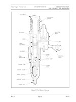
10. An ink-jet print head is schematically shown in Figure 4.20. The ink
jet consists of a heating element, ink channels, and a nozzle. Assume
the ink has the fluidic properties of water (
Table 4.8). The ink is ejected
due to bubble formation by heating the ink. When the bubble collapses,
the ink channel refills with ink. The square ink channels in the print
head are 20 µm. The ink jet ejects a 10-pL drop on each operating
cycle. Calculate the following:
a. The Reynolds number in the ink-jet nozzle when the 10-pL drop is
ejected in 20 µs
FIGURE 4.20 Thermal ink-jet print head.
heater
ink
(a) Thermal ink jet
20
µ
m
(b) Thermally ejecting a drop
(c) Bubble collapse – ink refilling
© 2005 by Taylor & Francis Group, LLC
152 Micro Electro Mechanical System Design
b. The Reynolds number in the ink jet when the ink channel is refilling
upon the collapse of the bubble. The refilling operation takes 200 µs.
c. From a thermal-scaling perspective, why are such rapid cycle times
possible in the ink jet?
d. If the ink-jet channels were decreased in size, would the thermal
cycle time increase or decrease?
11. A chemical sample has a concentration of 10
–6
mol/l. The detection
system has a detection sensitivity of ten molecules per liter.
a. What volume of sample is required?
b. If that volume is too big, what should be done?
c. What effect would increasing the sensitivity have on the required
sample size?
REFERENCES
1. J.W. Judy, Microelectromechanical systems (MEMS): fabrication, design and
applications, Smart Mater. Struct., 10, 1115–1134, 2001.
2. M.J. Madou, Fundamentals of Microfabrication, The Science of Miniaturization,
2nd ed., CRC Press, Boca Raton, FL, 2000.
3. J.D. Meindel, Q. Chen, J.A. Davis, Limits on silicon nanoelectronics for terascale
integration, Science, 293, 2044–2049, 14, September 2001.
4. W.T. Thompson, Theory of Vibrations with Applications, Prentice Hall, Inc., Engle-
wood Cliffs, NJ.
5. A. Lawrence, Modern Inertial Technology, Navigation, Guidance, and Control,
2nd ed., Springer-Verlag, Heidelberg, 156, 1998.
6. D.M. Tanner, N.F. Smith, L.W. Irwin. W.P. Eaton, K.S. Helgesen, J.J. Clement,
W.M. Miller, J.A. Walraven, K.A. Peterson, P. Tangyunyong, M.T. Dugger, S.L.
Miller, MEMS reliability: infrastructure, test structures, experiments, and failure
modes, SAND2000-0091, Sandia National Laboratories, January 2000.
7. N. Barbour, J. Connelly, J. Gilmore, P. Greiff, A. Kourepenis, M. Weinberg,
Micromechanical silicon instrument and systems development at per laboratory,
AAIA Guidance, Navigation Control Conf., San Diego, CA, 20–31 July 1996.
8. D.M. Tanner, J.A. Walraven, K.S. Helgesen, L.W. Irwin, D.L. Gregory, J.R. Stake,
N.F. Smith, MEMS a vibration environment, Proc. IRPS, 139–145, 2000.
TABLE 4.8
Water and Air Properties
Property Water Air @ STP
Mean free path l nm — 0.65
Surface tension s N/m 72 × 10
–3
—
Dynamic viscosity m kg/(m s) 10
–3
1.85 × 10
–5
Kinematic viscosity g m
2
/s 10
–6
1.43 × 10
–5
Density r kg/m
3
1000 —
© 2005 by Taylor & Francis Group, LLC
Scaling Issues for MEMS 153
9. D.M. Tanner, J.A. Walraven, K. Helgesen, L.W. Irwin, F. Brown, N.F. Smith, N.
Masters, MEMS reliability in shock environments, Proc. IRPS, 129–138, 2000.
10. C.M. Harris, C.E. Crede, Shock and Vibration Handbook, 2nd ed., McGraw-Hill
Book Company, New York, 1976.
11. J.P. Holman, Heat Transfer, 6th ed., McGraw–Hill Book Company, New York, 1986.
12. G.E. Karniadakis, A. Beskok, Micro Flows: Fundamentals and Simulation,
Springer, New York, 2002.
13. P. Bahukudumbi, A. Beskok, A phenomenological lubrication model of the entire
Knudsen regime, J. Micromech., Microeng., 13, 873–884, 2003.
14. J.L. Dohner, M. Jenkins, T. Walsh, K. Klody, Anomalies in the theory of viscous
energy losses due to shear in rotational MEMS resonators, Sandia National Lab-
oratories Report, SAND2003-4314, December 2003.
15. R.A. Syms, E.M. Yeatman, V.M. Bright, G.M. Whitesides, Surface tension-pow-
ered self-assembly of microstructures — the state of the art, J. MEMS, 12(4),
August 2003.
16. R.J. Smith, Circuits, Devices, and Systems, John Wiley & Sons Inc., New York,
1966.
17. C.T.A. Johnk, Engineering Electromagnetic Fields and Waves, John Wiley & Sons,
New York, 1988.
18. F. Paschen, Über die zum Funkenübergang in luft, Wasserstoff and Kohlensäure
bei verschiedenen Drücken erforderliche Potentialdifferenz, Weid. Ann. der Phys-
ick, 37, 69, 1889.
19. S.F. Bart, T.A. Lober, R.T. Howe, J.H. Lang, M.F. Schlecht, Design considerations
for micromachined electric actuators, Sensors Actuators, 14, 269–292, 1988.
20. B. Bollee, Electrostatic motors, Philips Tech. Rev., 30, 178–194, 1969.
21. I.J. Busch-Vishniac, The case for magnetically driven microactuators, Sensors
Actuators A, A33, 207–220, 1992.
22. A. O’Keefe, D.A.G. Deacon, Cavity ring-down optical spectrometer for absorption
measurements using pulsed laser sources, Rev. Sci. Instrum., 59, 2544–2551, 1988.
23. P.F. van Kessel, L.J. Hornbeck. R.E. Meier, M.R. Douglass, A MEMS-based
projection display, Proc. IEEE 86, 1687–1704, 1998.
24. D.M. Bloom, The grating light valve: revolutionizing display technology, Proc.
SPIE, 3013, 165–171, February 1997.
25. A. Manz, N. Graber, H.M. Widmer, Miniaturized total chemical analysis systems:
a novel concept for chemical sensing, Sensors Actuators, B1, 244–248, 1990.
26. K. Petersen, W. McMillan, G. Kovacs, A. Northrup, L. Christel, F. Pourahmadi,
The promise of miniaturized clinical diagnostic systems, IVD Technol., July 1998.
27. E. Oberg, Ed., Machinery’s Handbook, 24th ed., Industrial Press, New York, 2000.
28. G. Boothroyd, W.A. Knight, Fundamentals of Machining and Machine Tools,
Marcel Dekker, New York, 1989.
29. G.E. Moore, Cramming more components onto integrated circuits, Electronics,
38(8), April 19, 1965.
30. Y. Martin, C.C. Williams, H.K. Wickramasinghe, Atomic force microscope force
mapping and profiling on a sub 100Å scale, J. Appl. Phys., 61(9), 4723, 1987.
31. G. Benning, H. Rohrer, Scanning tunneling microscopy — from birth to adoles-
cence, Rev. Mod. Phys, 59(3), Part 1, 615, 1987.
32. J.A. Stroscio, D.M. Eigler, Atomic and molecular manipulation with the scanning
tunneling microscope, Science, 254, 1319–1326, 1991.
© 2005 by Taylor & Francis Group, LLC
154 Micro Electro Mechanical System Design
33. N. Taniguchi, Current Status in and future trends of ultraprecision machining and
ultrafine materials processing, Ann. CIRP, 32(2), 573–582, 1983.
34. G.L. Benevides, D.P. Adams, P. Yang, Meso-scale machining capabilities and
issues, Sandia National Laboratories report SAND2000-1217C, 2000.
35. A.H. Slocum, Precision Machine Design, Prentice Hall, Englewood Cliffs, NJ,
1992.
36. A.H. Slocum, Precision machine design: macromachine design philosophy and
its applicability to the design of micromachines, Proc. IEEE Micro Electro
Mechanical Syst. (MEMS ’92). Travemunde, Germany, 1992, 37–42.
37. R. Donaldson, S. Patterson, Design and construction of a large-axis diamond
turning machine, UCRL-89738, NTIS, 1983.
38. W.H. Press, B.P. Flannery, S.A. Teukolsky, W.T. Vetterling, Numerical Recipes in
C, The Art of Scientific Computing, Cambridge University Press, 1990.
39. K.J. Bathe, E.L. Wilson, Numerical Methods in Finite Element Analysis, Prentice
Hall, Inc., Englewood Cliffs, NJ, 1976.
40. O.C. Zienkiewicz, The Finite Element Method, McGraw-Hill Book Company,
New York.
41. ANSYS proposed system of units for MEMS scale simulation:
/>42. W.G. Knauss, I. Chasiotis, Y. Huang, Mechanical measurements at the micron and
nanometer scales, Mechanics Mater., 35, 217–231, 2003.
43. J.W. Hutchinson, Plasticity at the micron scale, Int. J. Solids Struct., 37, 225–238,
2000.
44. W.W. Van Arsdell, S.B. Brown, Subcritical crack growth in silicon MEMS, J.
MEMS, 8(3), 319–327, September 1999.
45. S. Quilici, G. Cailletaud, FE simulation of macro-, meso- and micro-scales in
polycrystalline plasticity, Computational Mater. Sci., 16, 383–390, 1999.
46. W.R. Runyan, K.E. Bean, Semiconductor Integrated Circuit Processing Technol-
ogy, Addison-Wesley, Reading, MA, 1990.
© 2005 by Taylor & Francis Group, LLC
155
5
Design Realization
Tools for MEMS
Just as MEMS fabrication has its roots in the microelectronics fabrication infra-
structure, the MEMS design realization infrastructure has its roots in the micro-
electronics infrastructure as well. However, the MEMS design realization require-
ments are significantly different. MEMS design involves complex geometric,
three-dimensional moving mechanical devices similar to macroworld machine
design. The result is a MEMS design realization environment that leverages a
significant portion from microelectronics while plotting a new path to meet the
new demands.
5.1 LAYOUT
The design of a device that is to be fabricated via LIGA, surface micromachining,
or bulk micromachining requires a mask to be made for the patterning step of
the fabrication process.
Figure 5.1 shows how the mask set, which is the interface
for the design engineer’s information (i.e., design), fits in the fabrication process
flow. A mask is a two-dimensional design representation that will be patterned
and etched into the working material. Bulk micromachining and LIGA products
typically require a minimal number of masks, typically only one or two masks,
to produce a high aspect ratio MEMS part. Surface micromachining can require
as many as 14 masks to produce a complex MEMS design. Thus, the three MEMS
fabrication technologies share a common need to interface design information
with the mask-making infrastructure; however, surface micromachining is more
complex due to the number of masks required. Surface micromachining will be
emphasized in this chapter because the complexities of design in this MEMS
fabrication technology is a superset of the issues involved with the others.
The infrastructure for mask making is an established industry primarily ser-
vicing the microelectronics production complex. The two common data formats
for the exchange of design layout information for use in the mask-making industry
are GDSII stream format [1] and the Cal Tech Intermediate Format (CIF) [2].
GDSII is a binary format and CIF is an ASCII format; both have become de facto
standards, but GDSII is much more prevalent.
Due to the geometric simplicity needed for microelectronics, the GDSII file
formation is merely a sequence of closed polygons that may be an approximation
© 2005 by Taylor & Francis Group, LLC