Microengineering MEMs and Interfacing - Danny Banks Part 9 pot
Bạn đang xem bản rút gọn của tài liệu. Xem và tải ngay bản đầy đủ của tài liệu tại đây (1.06 MB, 17 trang )
Microsensors 141
this form for long. It interacts with the oxygen entering through the membrane.
The products of this interaction are the oxidized form of the enzyme, two hydro-
gen ions, and two oxygen ions. When the platinum electrode is biased to the
correct potential, it will reduce one of the oxygen ions such that the end products
are oxygen and water. The resulting electrode current can be measured and will
be proportional to the concentration of glucose in the external medium. (Note
that this is a simplified explanation; there are also many other ways to monitor
the reaction).
One thing to note is that because the various molecules have to physically
move through the materials of the sensor, such biosensors can be quite slow to
respond to changes in the external medium.
5.6 MICROELECTRODES FOR NEUROPHYSIOLOGY
Microelectrodes of fine-wire or electrolyte-filled micropipettes have been
used for some time now to study the nervous system on a cellular (individual
neuron) basis. These, in particular the metal wire microelectrodes, are prime
targets for the application of microengineering techniques. The small signal
amplitudes involved (in the region of 100 µV) and high interface impedances
(1 to 10 MΩ at 1 kHz) between the metal and the tissue mean that it is advan-
tageous to place the amplifier as close as possible to the recording site. In addition,
the characteristics of microfabricated devices can be more reproducible than those
of handmade metal wire microelectrodes, and their small size enables the accurate
insertion of many recording sites into small volumes of tissue to study networks
of neurons or for neural prosthesis applications.
The microelectrodes operate by detecting the electrical potential generated
in the tissue near an active nerve fiber because of action potential currents flowing
through the fiber membrane. There are three common types of micromachined
microelectrode (Figure 5.9). Array-type microelectrodes (Figure 5.9a) are used
to form the floor of cell culture dishes: signals are recorded from neurons that
are placed or grown over these. Probe-type microelectrodes (Figure 5.9b) have
recording sites on a long thin shank that is inserted into the tissue under inves-
tigation. Regeneration electrodes (Figure 5.9c) are placed between the ends of a
severed peripheral nerve trunk; nerve fibers then regrow (regenerate) through the
device.
These microelectrodes can be quite difficult to use. For array microelectrodes,
appropriate cell culture methods have to be developed and practiced. Probe types
have to be mounted on amplifier boards, and different situations require probes
of many different shapes and size. Regeneration electrodes have to be fixed to
the stumps of the nerve trunk and are required to be connected to the outside
world. All devices can potentially generate huge amounts of data that have to be
collected and analyzed.
DK3182_C005.fm Page 141 Friday, January 13, 2006 10:59 AM
Copyright © 2006 Taylor & Francis Group, LLC
Microsensors 143
5.7 MECHANICAL SENSORS
Two different types of mechanical sensors will be discussed here. The first uses
physical mechanisms to directly sense the parameter of interest (e.g., distance
and strain). The second uses microstructures to enable the mechanical sensors to
detect parameters of interest (e.g., acceleration) that cannot be measured directly
with the first type of sensor.
5.7.1 PIEZORESISTORS
The change in resistance of a material with applied strain is termed the piezore-
sistive effect. Piezoresistors are relatively easy to fabricate in silicon, being just
a small volume of silicon doped with impurities to make it n type or p type.
Piezoresistors also act as thermoresistors, so to compensate for changes in
ambient temperature they are usually connected in a bridge configuration of some
sort with a dummy set; this is illustrated in Figure 5.10. Figure 5.10 illustrates
part of an accelerometer mass suspended by a beam from the bulk of the silicon
FIGURE 5.10 Piezoresistor configuration: (a) piezoresistors (dark rectangles) are
implanted into the beam suspending an accelerometer mass, seen from above, and a
reference pair are implanted on a dummy beam; (b) the four resistors are connected in a
bridge circuit. If all resistances match, then V
diff
will be 0 V. If the beam bends as a result
of acceleration, then R2 will change its resistance and the bridge circuit will no longer be
balanced.
R1 R2
R3 R4
(a)
V
dif
V
bridge
R4
R3
R2
R1
(
b
)
DK3182_C005.fm Page 143 Friday, January 13, 2006 10:59 AM
Copyright © 2006 Taylor & Francis Group, LLC
144 Microengineering, MEMS, and Interfacing: A Practical Guide
wafer (compare this with Figure 5.12, which shows a similar design in cross
section). Next to the suspension beam is a second beam, which is not attached
to the mass. Resistors have been implanted into both beams and the bulk of the
silicon substrate. These have been connected to form a bridge circuit (Chapter
11, Section 11.4 explains how this operates). Should the temperature change, the
close proximity of the four resistors ensures that they all experience the same
temperature and the bridge remains balanced. The use of the dummy beam not
connected to the mass is important because the resistor on the beam is in a slightly
different thermal than those implanted in the bulk of the wafer. Thus, only changes
in resistance induced by deformation of the beam will be registered.
5.7.2 PIEZOELECTRIC SENSORS
When a force is applied to a piezoelectric material, a charge proportional to the
applied force is induced on the surface. The applied force can thus be deduced
by measuring the electrical potential that appears across the crystal. Common
piezoelectric crystals used for microengineered devices include zinc oxide and
PZT (PbZrTiO3 — lead zirconate titanate), which can be deposited on micro-
structures and patterned.
5.7.3 CAPACITIVE SENSORS
For two parallel conducting plates separated by an insulating material, the capac-
itance between the plates is given by Equation 5.4, where A is the area of the
FIGURE 5.11 (a) A resonant bridge can be used to sense deformation, (b) when the
membrane is deformed, the resonant frequency of the bridge will change.
FIGURE 5.12 Bulk micromachined accelerometer in cross section — compare with
Figure 5.10 (not to scale).
(a) (b)
Membrane
Bridge
Support
Mass
Piezoresistor
Suspension
DK3182_C005.fm Page 144 Friday, January 13, 2006 10:59 AM
Copyright © 2006 Taylor & Francis Group, LLC
Microsensors 145
plates, d the distance between them, and ε a constant depending on the material
between the plates (this assumes that the circumference of the plates is much
larger than the distance between them, so what happens at the edges of the plates
can be neglected).
(5.4)
(For air, ε is approximately 8.9 × 10 − 12 F/m.) From this it can be seen that
the measured capacitance is inversely proportional to the distance between the
two plates. It is possible to use this technique to measure small displacements
(microns to tens of microns) with high accuracy (subnanometer); however, the
instrumentation required to measure capacitance changes can be a little complex.
The capacitor bridge, for example, is dealt with in Chapter 11, Subsection 11.4.1.
5.7.4 OPTICAL SENSORS
Silicon is a reflective material, as are other materials used in semiconductor device
fabrication (e.g., aluminum). Thus, optical means may be used to sense displace-
ment or deformation of microengineered beams, membranes, etc. A laser is
directed at the surface to be monitored in such a way that interference fringes
are set up. By analyzing these fringes, displacement or deformation may be
detected and quantified. One area in which optical sensing is often employed is
atomic force microscopy — to monitor the deflection of the beam upon which
the sensing tip is mounted (see discussion on scanning probe microscopy in
Chapter 10).
5.7.5 RESONANT SENSORS
These are based on micromachined beams or bridges that are driven to oscillate
at their resonant frequency. Changes in the resonant frequency of the device
would typically be monitored using implanted piezoresistors, capacitive, or
optical techniques.
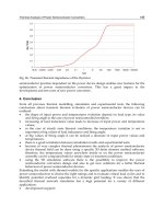
Figure 5.11a shows a bridge driven to resonance on a thin membrane. The
resonant frequency of the bridge is related to the force applied to it (between
anchor points), its length, thickness, width, mass, and the modulus of elasticity
of the material from which it has been fabricated. If the membrane that the bridge
is mounted on is deformed (Figure 5.11b), for instance, there is greater pressure
on one side than the other. Then the force applied to the bridge changes, and
hence the resonant frequency changes.
Alternatively, a resonant device may be used as a biosensor by coating it with
a material that binds to the substance of interest. As more of the substance binds
to the device, its mass will be increased, again altering the resonant frequency.
C
A
d
=ε
DK3182_C005.fm Page 145 Friday, January 13, 2006 10:59 AM
Copyright © 2006 Taylor & Francis Group, LLC
146 Microengineering, MEMS, and Interfacing: A Practical Guide
5.7.6 ACCELEROMETERS
Microengineered acceleration sensors, accelerometers, consist of a mass suspended
from thin beams (Figure 5.12). As the device is accelerated, a force (force = mass
× acceleration) is developed, which bends the suspending beams. Piezoresistors
situated where the beams meet the support (where strain is greatest) can be used
to detect acceleration. Another alternative is to capacitively sense the displace-
ment of the mass.
5.7.7 PRESSURE SENSORS
Microengineered pressure sensors are usually based on thin membranes. On one
side is an evacuated cavity (for absolute pressure measurement), and the other
side is exposed to the pressure to be measured. The deformation of the membrane
is usually monitored using piezoresistors or capacitive techniques.
DK3182_C005.fm Page 146 Friday, January 13, 2006 10:59 AM
Copyright © 2006 Taylor & Francis Group, LLC
147
6
Microactuators
6.1 INTRODUCTION
Microactuators are required to drive resonant sensors (see Chapter 5, Subsection
5.7.5) to oscillate at their resonant frequency. They are also required to produce
the mechanical output required of particular microsystems: this may be to move
micromirrors to scan laser beams or switch them from one fiber to another, to
drive cutting tools for microsurgical applications, to drive micropumps and valves
for microanalysis or microfluidic systems, or these may even be microelectrode
devices to stimulate nervous tissue in neural prosthesis applications.
In the following section a variety of methods for achieving microactuation
are briefly outlined: electrostatic, magnetic, piezoelectric, hydraulic, and thermal.
Of these, piezoelectric and hydraulic methods seem to be most promising,
although the others have their place. Electrostatic actuation runs a close third and
is possibly the most common and well-developed method, but it does suffer a
little from wear and sticking problems. Magnetic actuators usually require rela-
tively high currents (and high power) and, on the microscopic scale, electrostatic
actuation methods usually offer better output per unit volume (the limit is some-
where in the region of 1-cm
3
to few-cubic-millimeter devices depending on the
application). Thermal actuators also require relatively large amounts of electrical
energy, and the heat generated has to be dissipated.
When dealing with very smooth surfaces, typical of micromachined devices,
sticking or cold welding of one part to another can be a problem. These effects
can increase friction to such a degree that all the output power of the device is
required just to overcome it, and they can even prevent some devices from
operating. Careful design and selection of materials can be used to overcome
these problems, but they still cause trouble with many micromotor designs.
Another point to be aware of is that when removing micromachined devices from
wet-etch baths, the surface tension in the liquid can be strong enough to stick
parts together.
6.2 ELECTROSTATIC ACTUATORS
For a parallel plate capacitor, the energy stored,
U
, is given in Equation 6.1 (where
C
is the capacitance and
V
is the voltage across the capacitor).
(6.1)
UC
V
=
2
2
DK3182_C006.fm Page 147 Friday, January 13, 2006 10:59 AM
Copyright © 2006 Taylor & Francis Group, LLC
148
Microengineering, MEMS, and Interfacing: A Practical Guide
When the plates of the capacitor move toward each other, the work done by
the attractive force between them can be computed as the change in
U
with
distance
x
. The force can be computed using Equation 6.2:
(6.2)
Note that only attractive forces can be generated in this instance. Also, to
generate large forces (which will do the useful work of the device), a large change
of capacitance with distance is required. This has led to the development of
electrostatic comb drives (Figure 6.1).
6.2.1 C
OMB
D
RIVES
These are particularly popular with surface-micromachined devices. They consist
of many interdigitated fingers (Figure 6.1a). When a voltage is applied, an attrac-
tive force is developed between the fingers, which move together (Figure 6.1b).
The increase in capacitance is proportional to the number of fingers; so to generate
large forces, a large number of fingers are required. One problem with this
device is that if the lateral gaps between the fingers are not the same on both sides
FIGURE 6.1
Schematic of comb drive operation.
+
V
Flexible
support
Fingers of comb drive
(b)
(a)
F
VC
x
x
=
∂
∂
2
2
DK3182_C006.fm Page 148 Thursday, February 2, 2006 4:25 PM
Copyright © 2006 Taylor & Francis Group, LLC
Microactuators
149
(or if the device is jogged), then it is possible for the fingers to move at right angles
to the intended direction of motion and stick together until the voltage is switched
off (and in the worst-case scenario, they will remain stuck even after that).
For a comb drive with
N
electrodes (or rather, 2
N
gaps between the fingers),
the capacitance is approximately:
(6.3)
where
h
is the depth of the structure,
g
the gap between two electrode fingers,
x
the overlap of the two combs, and
ε
the permitivity. Thus:
(6.4)
6.2.2 W
OBBLE
M
OTORS
Wobble motors are so called because of the rolling action by which they operate.
Figure 6.2a and Figure 6.2b show a surface-micromachined wobble motor design.
The rotor is a circular disk. In operation the electrodes beneath it are switched on
and off one after another. The disk is attracted to each electrode in turn, the edge
FIGURE 6.2
Wobble motors: (a) a surface-micromachined type, (b) use of LIGA to
achieve a larger overlap between rotor and stator electrodes.
CNhx
g
≈ 2
ε
∂
∂
=
C
x
Nh
g
2
ε
Rotor
(a)
(Not to scale)
(b)
Stator
electrodes
Insulated stator
electrodes
To
p
view
Side view
DK3182_C006.fm Page 149 Friday, January 13, 2006 10:59 AM
Copyright © 2006 Taylor & Francis Group, LLC
150
Microengineering, MEMS, and Interfacing: A Practical Guide
of the disk contacting the insulator over the electrode. In this manner it rolls slowly
around in a circle, making one revolution to many revolutions of the stator voltage.
Problems can arise if the insulating materials on the stator electrodes wear rapidly
or stick to the rotor. Also, if the rotor and bearing are not circular (this is possible
because many CAD packages draw circles as many-sided polygons), then the rotor
can get stuck on its first revolution.
A problem with surface-micromachined motors is that they have very small
vertical dimensions, so it is difficult to achieve large changes of capacitance with
the motion of the rotor. LIGA techniques can be used to overcome this problem —
for instance, the wobble motor shown in Figure 6.2c and Figure 6.2d, where the
cylindrical rotor rolls around the stator.
6.3 MAGNETIC ACTUATORS
Microstructures are often fabricated by electroplating techniques, using nickel.
This is particularly common with LIGA. Nickel is a (weakly) ferromagnetic
material and so lends itself to use in magnetic microactuators. An example of
a magnetic microactuator is the linear motor shown in Figure 6.3. The magnet
resting in the channel is levitated and driven back and forth by switching
current into the various coils on either side of the channel at the appropriate
time.
From Figure 6.3, one common problem with magnetic actuators is clear:
the coils are two dimensional (three-dimensional coils are difficult to micro-
fabricate). Also, the choice of magnetic materials is limited to those that can
be easily micromachined, so the material of the magnet is not always optimum.
This tends to lead to a rather high power consumption and heat dissipation
for magnetic actuators. In addition, with microscopic components (up to about
millimeter dimensions), electrostatic devices are typically stronger than mag-
netic devices for equivalent volumes, whereas magnetic devices excel for larger
dimensions.
FIGURE 6.3
Magnetic actuator.
DK3182_C006.fm Page 150 Friday, January 13, 2006 10:59 AM
Copyright © 2006 Taylor & Francis Group, LLC
Microactuators
151
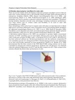
6.4 PIEZOELECTRIC ACTUATORS
The piezoelectric effect mentioned previously for use in force sensors also works
in reverse. If a voltage is applied across a film of piezoelectric material, a force
is generated. Examples of how this may be used are given in Figure 6.4. In Figure
6.4a, a layer of piezoelectric material is deposited on a beam. When a voltage is
applied, the stress generated causes the beam to bend (Figure 6.4b).
The same principle can be applied to thin silicon membranes (Figure 6.4c).
When a voltage is applied, the membrane deforms (Figure 6.4d). This, when
combined with microvalves, can be used to pump fluids through a microfluidic
system.
When fabricating piezoelectric devices, it is necessary to ensure that the films
are suitably thick so that high enough voltages can be applied without dielectric
breakdown (sparks or short circuits across the film).
6.5 THERMAL ACTUATORS
Thermal microactuators are commonly either of the bimetallic type or use the
expansion of a liquid or gas.
In Figure 6.5a, a beam is machined from one material (e.g., silicon) and a
layer of material with a different coefficient of thermal expansivity (e.g., alumi-
num).
When the two are heated, one material expands faster than the other, and
the beam bends (Figure 6.5b). Heating may be accomplished by passing current
through the device, thus heating it electrically.
Figure 6.5c shows a cavity containing a volume of fluid with a thin membrane
as one wall. The current passed through a heating resistor causes the liquid in
the cavity to expand, deforming the membrane (Figure 6.5d). The most effective
method of actuation is critical point heating. A liquid with a suitably low boiling
point is chosen and actuation is effected not merely through thermal expansion
of the liquid but by heating it to its boiling point. The large volume change that
FIGURE 6.4
Piezo actuators: (a) and (b) a cantilever beam; (c) and (d) an actuated
membrane.
V
+
(b)
(a)
V
+
(
d
)
(c)
DK3182_C006.fm Page 151 Friday, January 13, 2006 10:59 AM
Copyright © 2006 Taylor & Francis Group, LLC
Microactuators
153
6.7 MULTILAYER BONDED DEVICES
Surface micromachining (Chapter 2, Subsection 2.7.2) provides an obvious way
to build complex multilayered structures. The disadvantage of this approach
is that the vertical dimensions of the structures are usually quite small (on the
order of microns rather than hundreds of microns). A similar approach is available
for bulk micromachined devices, whereby bulk micromachined wafers are stacked
and bonded together. There are obvious problems with registration and alignment,
and devices constructed in this way are generally quite large. Figure 6.7 gives a
cross section through a hypothetical microfluidic device constructed using this
method.
6.8 MICROSTIMULATORS
One further method of actuation is illustrated by the use of microelectrode devices
to electrically stimulate activity of nerves and muscles. Common designs for these
devices have already been discussed in Chapter 5 (Section 5.6). The use of micro-
electrode devices facilitates highly specific stimulation of individual nerve fibers
compared to other methods of stimulation; this should allow finer control of the
stimulation provided enough electrode sites can be inserted into the tissue.
As relatively large stimulating currents have to be passed through the elec-
trode sites, microelectrodes for stimulation generally have geometrically larger
electrode sites than those for recording (500
µ
m
2
and above compared to 16
µ
m
2
and above). This is necessary, otherwise the currents involved will damage the
electrode sites.
One area in which silicon microengineering is being applied in the hope that
it will result in a considerable improvement over more conventional electrodes
is the area of visual prosthesis — providing rudimentary vision for the blind.
FIGURE 6.7
Microfluidic device constructed by bonding four bulk machined wafers
(cross section, not to scale); the inlet and outlet valves are formed by cantilever beams,
and a pump is created by deforming a membrane to change the volume of the pump
chamber.
Inlet
valve
Outlet
valve
Actuator
Pump
chamber
DK3182_C006.fm Page 153 Friday, January 13, 2006 10:59 AM
Copyright © 2006 Taylor & Francis Group, LLC
154
Microengineering, MEMS, and Interfacing: A Practical Guide
One project involves a “forest” of silicon needles that will be inserted in the
visual cortex.
Early visual prosthetic devices involved an array of electrodes placed on the
surface of the visual cortex (brain). When activated, blind volunteers could see
points of light (phosphenes). However, these devices required relatively high
currents to operate, and the image was distorted by afterdischarges and interac-
tions between groups of neurons. This led to the suggestion that a method for
more selective stimulation of neurons within the visual cortex was required to
provide any functional form of vision. So this is an area is which microengineering
technology is recently being applied.
DK3182_C006.fm Page 154 Friday, January 13, 2006 10:59 AM
Copyright © 2006 Taylor & Francis Group, LLC
155
7
Micro Total Analysis
Systems
7.1 INTRODUCTION
The term
micro total analysis system
(
µ
TAS) was originally coined by a group of
researchers to describe the kind of chemical processing system outlined in
Figure 7.1. This goes beyond chemical sensors or biosensors as it is modeled on
the analytical procedures often found in industry:
• Go to the site of investigation.
• Take samples.
• Return the samples to the laboratory.
• Prepare the samples: filter, centrifuge, and split up for different
processes.
• Perform analysis — this may involve a series of chemical reactions
and may even be performed by robots.
• Record examination results.
• Adjust the industrial process if necessary.
• Repeat as frequently as required.
Obviously, this is not always very convenient. For instance, water companies
want to know the results as soon as possible when there has been a pollution
incident — before the polluted water reaches the consumer and preferably before
there has been any major environmental damage. Furthermore, regular sampling
and analysis can be a very expensive process. Highly trained staff have to be
employed in an expensively equipped laboratory, and people must go regularly
to the appropriate sampling points, which may be long distances apart in the case
of large companies or for some systems. Many processes involve hazardous
chemicals that are very difficult to sample, transport, and dispose of. The same
may be said of the chemical reagents used to analyze the sample, and these may
also be very expensive. In the worst situation, the entire manufacturing process
may need to be shut down to enable it to be investigated properly.
Given all these challenges, it is not surprising that microengineering tech-
niques were applied to the area of chemical analysis quite early on. In fact, one
of the first commercial applications (developed in the 1970s) was the Stanford
gas chromatograph, developed by Terry, Jerman, and Angell. This provided a
system for separating and detecting gases in a sample on a single silicon wafer.
The main focus in this chapter will be on the core elements of
µ
TAS — the
microfluidic, electrophoretic separation systems that it employs, and the detection
DK3182_C007.fm Page 155 Thursday, January 19, 2006 11:17 AM
Copyright © 2006 Taylor & Francis Group, LLC
Micro Total Analysis Systems
157
7.2.1 I
NORGANIC
C
HEMISTRY
Any exploration of chemistry starts with the Periodic Table of Elements, such as
that shown in Figure 7.2. For simplicity, Figure 7.2 only shows a subsection of
the Periodic Table.
Matter is composed of atoms of the different elements, which combine (react)
according to known rules. Atoms are composed of three types of subatomic parti-
cles: protons and neutrons, which are found in the center (nucleus) of the atom,
and electrons, which form a cloud around the nucleus. The protons in the nucleus
each carry one unit of positive charge, and the electrons each carry one unit of
negative charge. The
atomic number
(Figure 7.2) of the element is the number of
protons in the nucleus. In a normal atom, the number of electrons in the atom is
equal to the number of protons, and the atom carries zero charge. In certain
circumstances, it is possible to add or remove electrons from the atom; the resulting
charged particle is called an
ion
.
The electrons crowd near the nucleus, and as the number of electrons in the
atom increases, not all of them get an equal share of the nucleus. It is convenient
to consider the electrons as existing in different energy shells — related to the
amount of energy required to remove them from the atom. For an atom with a
lot of electrons, it is relatively easy to remove the first one (ionize the atom), but
as more and more electrons are removed, more and more energy is required.
The basic rule of chemistry is that an atom would like to fill its outer shell with
electrons (this being, energetically, the most preferable state to be in). However, if
it were to simply add or shed electrons at a whim, matter would be electrically
charged. But matter (on the macroscopic scale and, in general, over time) remains
electrically neutral. It has already been noted that it takes energy to ionize an atom,
and in the absence of that energy, electrons will simply flow from negatively charged
areas to positively charged ones so that both become neutral. The atom, therefore,
has two options to achieve this neutral state. Either it can borrow electrons from
another atom (or atoms), in which case the resulting ions must stay close together
to ensure their charges cancel out and give an overall appearance of neutrality, or
it can share electrons with another atom (or atoms), in which case the atoms must
stay so close together that a single electron cloud can envelop them.
Amount of Substance
Elements also have an associated mass number. This is the number of protons
plus neutrons in a sample of the element as it naturally occurs. It is not always
exactly twice the atomic number, as may be expected, because many elements
exist as different isotopes with slightly different numbers of neutrons. The
relative abundance of these isotopes gives rise to noninteger atomic masses.
The atomic mass of an element expressed in grams is one molar mass (
M
) of
the element and contains 6.02
×
10
23
atoms (this is the Avogadro constant).
1
M
dissolved in 1 l of water gives a solution of 1-mol concentration.
DK3182_C007.fm Page 157 Thursday, January 19, 2006 11:17 AM
Copyright © 2006 Taylor & Francis Group, LLC
158
Microengineering, MEMS, and Interfacing: A Practical Guide
This gives rise to two kinds of bonds: the
ionic bond
, formed between ions,
and the
covalent bond
, formed when electrons are shared equally between atoms.
The number of electrons that comprise a full outer shell can be determined
from the group in which the element appears in the Periodic Table (Figure 7.2);
this has been summarized in Table 7.1. The notable exception is hydrogen. It
normally loses an electron to form a positive hydrogen ion, but it can form a
negatively charged hydronium ion.
Figure 7.2 shows two divisions: metals and nonmetals; semimetals can be
found along the line on the nonmetal side. Compounds formed when metals
react with nonmetals form ionic bonds. Atoms of nonmetallic elements combine
by forming covalent bonds. The elements in group I and group VII are generally
more reactive than those in the other groups. Elements in group VIII are the
most inert, and these are the only gaseous elements that can be found in their
atomic state under normal conditions; all the others forms combine into mol-
ecules (oxygen atoms pair up, for instance, to form oxygen molecules). In the
solid state, atoms are bonded together into some sort of crystalline or amorphous
structure.
Pure elemental metals do not form either ionic or covalent bonds. Rather,
they exist in a state in which the electrons in the outer shells escape from the
influence of the particular nucleus, so the atoms in a metal can be considered
as floating in a sea of electrons; this is why metals conduct electricity so well.
In semiconductors, there is sufficient energy at room temperature to enable
electrons to occasionally escape from the influence of a particular nucleus, but
they are soon captured by another; thus, they conduct electricity but not as well
as metals do.
TABLE 7.1
Number of Electrons Required to Complete the Outer Shell
Group
Electrons in the
Outer Shell
Gain (+) or Lose
(-
) to Get a Full
Outer Shell Notes
I1
−
1 Hydrogen sometimes gains
one
II 2
−
2
III 3
−
3
IV 4
+
4 or
−
4
V5
+
3
VI 6
+
2
VII 7
+
1
VIII 8 0 Helium has, and requires,
only two; it does not readily
react with anything
DK3182_C007.fm Page 158 Thursday, January 19, 2006 11:17 AM
Copyright © 2006 Taylor & Francis Group, LLC
Micro Total Analysis Systems
159
7.2.1.1 Bond Formation
Chemical reactions between elements in group I or group II with elements in
group VII will form ionic bonds.
Common table salt, sodium chloride, is formed from one atom of sodium
combining with one atom of chlorine. As suggested from Table 7.1, the sodium
atom gives up an electron to become a sodium ion (denoted as Na
+
), and the
chlorine atom gains an electron, becoming a chlorine ion (Cl
−
); the two ions
combine to form the compound, thus:
Na
+
Cl
→
NaCl (7.1)
Magnesium, however, loses two electrons (becoming Mg
2+
), and these ions
are accepted by two chlorine atoms:
Mg
+
2Cl
→
MgCl
2
(7.2)
The movement of electrons is not normally explicitly stated in chemical equa-
tions unless they are provided from an unusual source, such as an electric current
from an electrode, or if the equation needs to be broken down for some reason.
The metals of group I burn well in air and react violently with water (H
2
O,
a combination of hydrogen and oxygen); for this reason, they are stored under
oil. The relevant equations for potassium are:
2K
+
O
→
K
2
O (7.3)
and
2K
+
2H
2
O
→
2KOH
+
H
2
(7.4)
Similarities between Elements
This section has been written in a way that suggests that the chemical properties
of an element follow from its position in the Periodic Table. The historical truth
is that the table was originally developed by grouping elements that exhibited
similar chemical properties. It was only later that these were formally related
to atomic structure in the manner described.
Combination of Sodium and Chlorine
In more detail, showing the formation of sodium and chloride ions and the
transfer of electrons, Equation 7.1 develops as follows:
Na
→
Na
+
+
e
−
sodium ion formation
Cl
+
e
−
→
Cl
−
chloride ion formation, using the electron given up by Na
Na
+
+
Cl
−
→
NaCl two charged ions combine into a neutral compound
DK3182_C007.fm Page 159 Thursday, January 19, 2006 11:17 AM
Copyright © 2006 Taylor & Francis Group, LLC
160
Microengineering, MEMS, and Interfacing: A Practical Guide
Notice that in Equation 7.4, a hydrogen molecule (H
2
) has been given off by
the reaction. The other product of the reaction, potassium hydroxide, is formed
from the combination of a potassium (K
+
) ion and a hydroxide (OH
−
) ion. Where
elements naturally occur in molecular form, then it is normal to show this in the
chemical equation. Equation 7.1 to Equation 7.3 thus become:
2Na
+
Cl
2
→
2NaCl (7.5)
Mg
++
Cl
2
→
MgCl
2
(7.6)
4K
+
O
2
→
2K
2
O (7.7)
Covalent-bond formation arises due to the sharing of electrons. In Equation 7.5
and Equation 7.6 it has been suggested that chlorine forms a molecule of two
chlorine atoms. Because chlorine is a nonmetal, this involves the formation of a
covalent bond. From Table 7.1 and Figure 7.2, it can been seen that chlorine has
seven electrons in its outer shell; it would like to have eight. It can achieve this
by sharing a pair of electrons with another chlorine molecule, with each atom
donating one of the pair, as shown in Figure 7.3. (Obviously, it is not possible
to tell which electron came from which atom, as illustrated.)
This sharing of a pair of electrons forms a single covalent bond, which is
graphically depicted by a single line (Figure 7.3). Two nitrogen atoms, on the other
hand, have to share three pairs, which results in a very strong triple bond; carbon
burns in air to form carbon dioxide, with two double bonds (see Figure 7.4).
Because the electrons are shared between atoms in a covalent bond, they
cannot be everywhere at once. As a result, at any one time, one part of the resulting
molecule will be slightly negative and another part will be slightly positive. This
gives rise to a very weak form of intermolecular bonding, termed
van der Waals
bonding
. When the atoms in the molecule are of different elements, carbon and
chlorine for example, then it may well be that one component of the molecule is
more attractive to electrons than the other. In the case of carbon tetrachloride
FIGURE 7.3
(a) Two chlorine atoms form a bond by sharing a pair of electrons, (b) this
bond can also be drawn as a straight line.
FIGURE 7.4
(a) Nitrogen molecule, (b) carbon dioxide molecule.
Cl Cl
Cl
Cl
(
a
)(
b
)
(b)
OCO
(a)
NN
NN
OCO
DK3182_C007.fm Page 160 Thursday, January 19, 2006 11:17 AM
Copyright © 2006 Taylor & Francis Group, LLC