Microsensors, MEMS and Smart Devices - Gardner Varadhan and Awadelkarim Part 4 pdf
Bạn đang xem bản rút gọn của tài liệu. Xem và tải ngay bản đầy đủ của tài liệu tại đây (2.12 MB, 30 trang )
MONOLITHIC
PROCESSING
73
conductivity.
In
addition,
SOI
technology
offers
extremely
low
unwanted parasitic
effects
and
excellent isolation between devices (see Section 4.3.5).
4.3.1 Bipolar
Processing
The
bipolar
process
has
evolved
over
many years,
as has its
so-called
standard process.
Clearly, this
is an
important issue
and the
integration
of a
microsensor,
or
microactuator,
will
depend
on the
exact details
of the
process that
is
employed.
As
stated earlier,
the
possible approaches
to
microsensors
and
MEMS integration
and the
problems associated
with
compliance
to a
standard process
are
both discussed
in
some detail
in
later chapters.
This section presents what
may be
regarded
as the
standard bipolar process, which
employs
an
epi-layer
to
make
the two
most important types
of
bipolar components; that
is,
vertical
and
lateral transistors. Bipolar n-p-n transistors
are the
most commonly
used
components
in
circuit design
as
both amplifiers
and
switches because
of
their superior
characteristics compared with p-n-p transistors.
Let us now
consider
in
detail
the
process
steps required
to
make
a
vertical n-p-n
and
lateral p-n-p transistors.
A
similar process
can
be
defined
to
make vertical p-n-p transistors
or the
simpler substrate p-n-p transistors
with
slightly
different
device characteristics.
Worked
Example
E4.1: Vertical
and
Lateral Bipolar Transistors
The
standard bipolar process begins
by
taking
a
p-type substrate (i.e. single-crystal
silicon
wafer)
with
the
topside polished
2
.
A
buried n-layer
is
formed
within
the
p-type
substrate
by first
growing
an
oxide
layer.
The
oxide
is
usually
grown
in an
oxidation
furnace
using
either
oxygen
gas
(dry oxidation)
or
water
vapour
(wet
oxidation)
at a
temperature
in the
range
of 900 to
1300
°C. The
chemical
reactions
for
these
oxidation
processes
are as
follows:
Si(s)
+
2H
2
O(g) SiO
2
(s)
+
2H
2
(g) (4.6)
Other
ways
of
forming
an
oxide layer,
such
as
CVD,
are
discussed
in
Chapter
5.
The
thermal oxide layer
is
then patterned using
a
process called
lithography.
A
basic
description
of
these processes
is
given
in
this chapter
and a
description about
more
advanced
lithographic techniques
is
given
in
Chapter
5.
Lithography
is the
name
used
to
describe
the
process
of
imprinting
a
geometric pattern
from
a
mask onto
a
thin
layer
of
material,
a
resist,
which
is a
radiation-sensitive
polymer.
The
resist
is
usually
laid
down
onto
the
substrate
using
a
spin-casting
technique
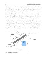
(see Figure 4.10).
In
spin-casting technique,
a
small volume
of the
resist
is
dropped onto
the
centre
of
the
flat
substrate, which
is
accelerated
and
spun
at a
constant
low
spin speed
of
about
2000
rpm to
spread
the
resist uniformly.
The
spin speed
is
then rapidly increased
to its
final
spin
speed
of
about
5000
rpm,
and
this stage
determines
its final
thickness
of 1 to
2
um. The
thickness
of the
spun-on resist,
d
R
, is
determined
by the
viscosity
77 of the
2
Double-sided
wafers
are
used
if a
back-etch
is
required
to
define
a
microstructure.
74
STANDARD
MICROELECTRONIC TECHNOLOGIES
Pipette
Spin
Liquid
Wafer
Motor
Vacuum
line
Figure 4.10
Apparatus
used
to
cast
a
resist
onto
a
substrate
in
preparation
for
optical
lithography
resist
and final
spin
speed
v
approximately according
to
^R
= -?= x /sc
(4.7)
where
f
sc
is the
percentage
solid
content
in
solution.
The
resist-coated
wafer
is
then cured
by
a
soft-bake
at a low
temperature
(80 to
100°C
for 10 to 20
minutes)
and a
process
mask
applied
for
shadow
or
projection printing
3
.
The
mask
is
generally
a
reticule mask
plate
and
comprises
a
glass
plate coated with
a
light-blocking material, such
as a
thin
chromium
film,
that
has
itself
been patterned using
a
wet-etching
process
and a
second
resist,
but in
this case
the
resist
has
been written
on
directly
using
a
high-resolution
electron-beam writer. Then
the
mask
and
substrate
are
exposed
to a
radiation source,
usually ultraviolet (UV) light,
and the
radiation
is
transmitted through
the
clear
parts
of
the
mask
but
blocked
by the
chromium coating.
The
effect
of the
radiation depends
on the
type
of
resist
-
positive
or
negative. When
a
positive resist
is
exposed
to the
radiation,
it
becomes soluble
in the
resist developer
and
dissolves leaving
a
resist pattern
of the
same shape
as
that
of the
chromium
film.
Conversely,
the
negative resist
becomes
less
soluble
when exposed
to the
radiation
and so
leaves
the
negative
of the
chromium coating.
Negative resists
are
used more commonly
as
they yield better results. Table
4.3
shows
some commercially available
resists
for
both optical
and
electron-beam lithography
4
.
Figure 4.11 shows
the
lithographic patterning
of a
substrate with
a
negative resist
and
chrome mask plate (mask
1), and
subsequent soft-baking
and
developing
in
chemicals,
to
leave
the
resist over
predefined
parts
of the
oxide layer.
The
resist
is
then hard-baked
3
Optical
and
other lithographic techniques
are
described later
in
Section 5.3.
4
These
terms
are
defined
later
on
under
bipolar
transistor
characteristics.
MONOLITHIC
PROCESSING
75
Table
4.3
Some commercially available resists
Resist
Kodak
747
AZ-1350J
Shippley
S-1813
PR
102
COP
PMMA
PBS
Lithography
Optical
Optical
Optical
Optical
E-beam
and
X-ray
E-beam
and
X-ray
E-beam
and
X-ray
Type
Negative
Negative
Negative
Positive
Negative
Positive
Positive
Mask
Wafer
Exposing radiation
Glass
Chromium
(80 nm)
An
image-forming system
may
occupy
a
portion
of
this space
Resist
Oxide
or
mulptiple layers
of
device
Wafer
substrate
Resist
Figure 4.11
Use of
radiation
and a
mask plate
to
create windows
in a
resist layer through which
the
oxide
is
etched
and
arsenic-doped
to
form buried n-regions
in a
p-type substrate.
The
buried
regions
are
used
to
increase device performance
(110
to 130 °C for 10 to 20
minutes)
and the
oxide
is
selectively removed using either
a
wet-etching
or a
dry-etching process.
Table
4.4
shows
the wet or
liquid etchants commonly used
to
remove
oxides
and
other
materials during
a
standard
process.
Dry
etching
is
becoming increasingly popular,
and
the
details
of
different
wet and dry
etching processes, which
are
often
referred
to as
micromachining
techniques,
are
described
in
this Chapter.
Next,
arsenic
is
introduced into
the
exposed p-type silicon regions. There
are two
different
techniques used: thermal
predeposition
and ion
implantation.
In
thermal predeposition,
a
powder, liquid,
or gas can be
used
as the
source dopant
material
for the
predeposition process.
The
solid solubility
of the
dopant
in the
material,
predeposition time,
and
temperature determine
how far the
dopant
diffuses
into
the
wafer.
For a
constant source concentration
C
s
, the
dopant concentration
at
distance
x and at
time
76
STANDARD
MICROELECTRONIC TECHNOLOGIES
Table
4.4
Some
wet
etchants used
in
processing
wafers
for
semiconductor
devices
Material
to
etch Composition
of
etchant
Etch
rate Temperature
(nm/min)
(°C)
Thermal
SiO2
Deposited
SiO2
Polycrystalline silicon
Aluminum
Buffered
oxide etch
4: 1 to
7:1
NH4F/HF(49%)
3:3:2 NF
4
F/acetic
acid/water
1:50:20
HF/HNO
3
/water
or
KOH
50:10:2:3
Phosphoric
acid/acetic
acid/nitric
acid/water
80-120
180-220
350-500
200-600
20-30
20-30
20-30
20-40
Silicon nitride Phosphoric acid 5-7.5
160-175
Table
4.5
Source materials
for
doping silicon substrates
Element
\/D at
Solid Compound
1100°C
solubility
at
name
(um
1150°C
State
Use
n-type:
Antimony
Arsenic
0.110
7xl0
19a
0.090
1.8 x
10
21
Antimony
trioxide Solid
Arsenic trioxide Solid
Subcollector
Closed tube
or
source
furnace;
subcollector
Phosphorus
p-type:
Boron
Arsine
0.329
1.4X10
21
Phosphoric
pentoxide
Phosphoric
oxychloride
Phosphine
Phosphoric
oxychloride
Silicon
pyrophosphate
Silicon
pyrophosphate
0.329
5 x
lO
20a
Boron trioxide
Boron tribromide
Diborane
Boron nitride
Gas
Solid
Liquid
Gas
Liquid
Solid
Solid
Solid
Liquid
Gas
Solid
Subcollector/emitter
Emitters
Emitters
Emitters
Emitters
Wafer
source
Wafer
source
Base/isolation
Base/isolation
Base/isolation
Wafer
source
a
At
1250°C
t,
C(x,
t), is
determined
by the
following
equation:
C(x,
t) = C
s
erfc
(4.8)
where
D is the
diffusion
coefficient.
Table
4.5
shows
the
different
sources used
to
dope semiconductors.
After
predeposition,
there
is a
drive-in step
in
which
the
existing dopant
is
driven into
the
silicon
and a
MONOLITHIC
PROCESSING
77
protective layer
of
oxide
is
regrown
in an
oxygen atmosphere.
In
practice,
the
diffusion
coefficient
D
does vary itself with
the
level
of
doping, increasing somewhat linearly with
arsenic
and
quadratically with phosphorus.
As a
result, calibrated charts, instead
of a
simple mathematical formula,
are
used
to
determine
the
doping profiles.
In
the
second doping technique, namely,
ion
implantation,
the
dopant element
is
ionised,
accelerated
to a
kinetic energy
of
several hundred keV,
and
driven into
the
substrate. This
alternative
method
is
discussed
in
Section 2.5.2.
After
predeposition
and
drive-in steps,
the
oxide protection layer
is
stripped
off
using
a
wet
or dry
etch
to
leave
the
n-regions
defined
in the
p-type substrate.
An
n-type epi-layer
of
4 to 6 um in
thickness
is
grown
on top of the
substrate (see Section 4.2.3)
to
create
the
buried n-type areas within
the
p-type substrate.
The
buried n-layer
is
used
to
minimise
both
the
collector series resistance
of the
vertical n-p-n transistor that
is
formed later
and
the
common-base (CB) current gain,
F
, of the
parasitic
p-n-p transistor formed
by the
collector
and
base
of the
lateral p-n-p transistor
and the
substrate. However,
the
buried
n-regions
can
diffuse
further into
the
epi-layer
at
elevated
temperatures,
and so
caution
is
required
in any
subsequent processing.
The
transistors need
to be
electrically
separated
from
each
other,
and
there
are a
number
of
techniques
with
which
to do
this. Common techniques used
are
oxide isolation, based
on
local
oxide
isolation
of
silicon
(LOCOS), junction isolation (JI)
based
on a
deep
boron
dope,
or
trench isolation, which
is
useful
for
minimising parasitic capacitance.
At
this
stage,
a
second mask (mask
2) is
used
to
define
the
regions into which boron
is
implanted
and
thus
isolate
one
transistor
from
another (see Figure 4.12).
Then
the
deep
n
+
-type
contacts
of the
vertical
n-p-n
collector
and
lateral
p-n-p
base
are
defined
using
a
third mask
in
another patterning process, followed
by an
extrinsic
p-type implant
for the
base
of the
vertical n-p-n transistor
and for
both
the
emitter
and
collector
of the
lateral p-n-p transistor (mask
3). The
relatively thick, highly doped
extrinsic layer
is
followed
by a
thinner, lighter doped intrinsic base implant (mask
4)
below
the
emitter
in the
vertical n-p-n transistor.
The
lighter doping provides
for a
large
common-emitter (CE) current gain
B
F
.
Next,
the
heavily doped
n
+
contact
to the
emitter
in the
vertical n-p-n transistor
is
implanted (mask
5) to
complete
the
transistor structures. Finally,
the
oxide layer
is
patterned (mask
6) to
form
contact holes through
to the
transistor contacts
and
substrate,
and
then
the
metal interconnect (normally
100 to 300 nm of
aluminum)
is
deposited either
by
physical evaporation
or by
sputtering
and is
patterned (mask
7) to
form
the
completed
IC.
Figure 4.13 shows
the
side view
of two
devices:
the
vertical n-p-n transistor
and
lateral p-n-p transistor.
In
some cases,
a
passivation layer
of
SiO2
or
some other material
is
deposited
and
patterned
(mask
8) to
serve
as a
physical
and
chemical protective barrier over
the
circuit.
This depends upon
the
proposed method
of
packaging
of the die
(see Section 4.4)
and
the
subsequent use.
The
complete bipolar process described here
is
summarised
in
Figure
4.14.
It
could
be
simplified
by
fabricating,
for
example,
a
pure n-p-n bipolar process, and,
in
fact,
most
of the
transistors
in
monolithic
ICs are
n-p-n structures. However, although
the
characteristics
of
p-n-p transistors
are
generally inferior
to an
n-p-n transistor,
as
stated
in
the
preceding text, they
are
used
as
active devices
in
operational
amplifiers,
and as the
injector
transistors
in the IIL
mentioned earlier. Similarly,
a
substrate p-n-p transistor
78
STANDARD
MICROELECTRONIC TECHNOLOGIES
Figure 4.12 Formation
of an
isolation region (p
+
)
in the
substrate
to
separate devices electrically
in
a
bipolar process.
The
isolation regions
are
used
to
enhance packing densities
Figure
4.13
A
vertical n-p-n transistor
and
lateral p-n-p transistor formed
by a
standard bipolar
process
MONOLITHIC PROCESSING
79
Figure
4.14 Standard bipolar process
to
make
a
vertical n-p-n transistor
and
lateral p-n-p
transistor
80
STANDARD MICROELECTRONIC
TECHNOLOGIES
Top
view
Side
view
(a)
II
n,
n epi
n
+
Buried layer
(b)
r°-
n
epi
-
A
{ n
+
Buried layer
n
epi
Figure 4.15 Various kinds
of
diodes available
from
a
bipolar process:
(a)
emitter-base;
(b)
base-collector;
and (c)
epi-isolation
rather than
a
lateral p-n-p transistor could
be
fabricated
by
leaving
out the
buried
n
+
-
layer.
The
problem that arises then
is
that
it
restricts
the
possible
circuit configurations
(because
the
collector
is
connected
to the
substrate that gives parasitic problems) and,
therefore,
the
process
can no
longer
be
regarded
as
standard.
Various
other components
can
also
be
formed
using
this bipolar process.
For
example,
Figure
4.15 shows three
different
types
of
diode that
can be
formed, namely,
the
emitter-
base diode that
has a low
reverse breakdown voltage
of 6 to 60 V and can be
used
as a
Zener
diode;
the
base-collector
diode that
has a
higher reverse breakdown voltage
of 15
to
50 V; and the
epi-isolation diode.
Figure 4.16 shows
five
different
types
of
resistor that
can be
formed:
the
base resistor
with
a
typical sheet resistance
of 100 to 500
/sq,
the
pinched-base resistor
with
a
typical
sheet resistance
of
2000
to
10000
/sq,
the
emitter resistor with
a
typical sheet resistance
of
4 to 20
/sq,
the
epi-resistor
with
a
sheet resistance that varies
from
400 to
2000 /sq,
and
a
pinched
epi-resistor
that
has a
higher sheet resistance than
an
epi-resistor
of 500 to
2000
/sq and is
often
used
in
preference
to the
latter.
Finally,
different
capacitors
can be
formed; Figure 4.17 shows both
the
dielectric capac-
itor,
in
which
the
thermal oxide
or
thinner emitter oxide
is
used
as the
dielectric,
and
the
junction capacitance, which
is
suitable when there
is no
requirement
for low
leakage
MONOLITHIC PROCESSING
81
(a)
(b)
(c)
Top
view Side
view
1
I
m
i
I
1
\
1
I
u
S
\I\
F3
1
yd
1
1
fit
1
1
p^i
1
42
r~h
n epi
n
+
Buried layer
r
1
-
(d)
n epi
(e)
l
'
LJ
l
'
n
epi
Figure
4.16 Various kinds
of
resistors available
from
a
bipolar
process:
(a)
base
resistor;
(b)
pin-
ched base resistor;
(c)
emitter resistor;
(d)
epi-resistor;
and (e)
pinched epi-resistor
currents
or a
constant capacitance.
In
general, these components tend
to
have inferior elec-
trical properties compared
with
discrete devices that
are
fabricated
by
employing other
technologies; therefore, extra care
is
required
to
design circuits using these components.
It
is
common
to use
discrete components
as
external reference capacitors
and
resistors
together
with
an 1C to
achieve
the
necessary performance.
82
STANDARD MICROELECTRONIC TECHNOLOGIES
Top
view
(a)
Side View
Aluminium
n
epi
(b)
n
epi
Figure
4.17
Two
types
of
capacitors
that
are
available
from
a
bipolar
process:
(a)
dielectric
and
(b)
junction
4.3.2
Characteristics
of
BJTs
As
noted earlier, there
are a
number
of
electronic devices available
from
a
bipolar process,
and
these
may be
used either
as
discrete components
or as
part
of an IC,
such
as an
oper-
ational amplifier
or
logic switch. Here,
a
basic
discussion
of the
characteristics
of the
bipolar transistor
is
presented. There
are
many textbooks that cover
different
aspects
of
the
bipolar transistor
from
the
basic
(e.g.
Sze
1985) through
to an
advanced treat-
ment
of the
device physics,
the
construction
of
sophisticated models (e.g. Hart 1994),
and
bipolar circuitry. Most
of
this material
is
outside
the
scope
of
this book, because
here
we are
mainly interested
in the
technologies
that
are
relevant
to the
integration
of
standard
ICs
with microtransducers
and
MEMS devices. However,
it is
necessary
to
include some basic material
on
bipolar
devices
for
three
reasons:
First,
as a
background
material
to the
readers
who are
less
familiar with electrical engineering topics
and who
want
to
know more about
the
basic electrical properties
of a
junction diode
and
tran-
sistor
and the
technical terms used, such
as
threshold voltage
or
current gain; second,
to
serve
as a
reminder
to
other readers
of the
typical characteristics
of a
bipolar device
for
use
when designing
an IC.
Finally,
and
perhaps most important,
to
provide back-
ground
information
on
microelectronic
devices that
can be
exploited directly,
or
within
an
1C, as a
microtransducer
or
MEMS device.
For
instance,
a
bipolar diode
or
bipolar
transistor
may be
used
to
measure
the
ambient temperature (see Chapter
8).
Therefore,
for
all
these reasons,
a
brief discussion
of the
properties
of the
bipolar junction
and
FETs
is
given here.
The
basic properties
of a
semiconducting material have already been discussed
in
Section
3.3 and
they should
be
familiar
to an
electrical
engineer
or
physicist. Therefore,
we
start
our
discussion with
the
properties
of the
junction diode before moving
on to the
BJT.
As
shown
in the
last
section,
a
junction diode
can be
fabricated
from
a
standard
bipolar process
by
forming
a
contacting region between
an
n-type
and
p-type material.
MONOLITHIC
PROCESSING
83
Figure 4.18 shows
(a) a
schematic
of the
structure
and (b) its
symbol
and
implementation
in
a
simple direct current (DC) circuit.
The
concentration
of the
donors
and
acceptors
are
shown
in
Figure 4.18(c).
In
the
absence
of an
external voltage
V
applied across
the
diode, there
is a
tendency
for
acceptors
in the
p-type material
to
diffuse
across into
the
n-type region driven
by the
difference
in
electrochemical
potential caused
by the
high concentration
of
acceptors
p
p
in
p-type region compared with that
in the
n-type region
n
p
(i.e.
p
p
»
n
p
). Similarly,
there
is a
tendency
for the
donors
in the
n-type material
to
move into
the
p-type material
because
of the
mismatch
in
carrier concentration, namely
n
n
>> p
n
.
Because
no
current
can
flow
across
the
junction without
an
external voltage,
a
depletion region that
is
free
of
mobile charge carriers
is
formed. This region
is
called
the
space
charge region
and
it
is
shown
in
Figure 4.18(c), where
the
region near
the
p-type material
is
left
with
a
net
negative charge
and the
region near
the
n-type material
is
left
with
a net
positive
charge.
Together, these
form
a
dipole layer
and
hence
a
potential barrier
of
height
V
d
(Figure 4.18(d)) that prevents
the flow of
majority carriers
from
one
side
to the
other.
The
height
of the
potential barrier, which
is
also known
as the
diffusion
potential
or
contact
potential,
is
determined
by the
carrier concentrations
q P
P
(4.9)
where
T is the
absolute temperature
and q is the
charge
on an
electron.
The
diffusion
potential
varies
for
different
technologies
and is
about
0.5 to 0.8 V for
silicon,
0.1 to
0.2 V for
germanium,
and
about
1.5 V for
GaAs.
(a)
p-type
n-type
aia^i^fijggg;'^
(d)
Space-charge
region
Figure 4.18 Schematic diagram
of (a) a p-n
junction diode;
(b)
equivalent symbol;
(c)
space-
charge region;
(d)
contact potential
84
STANDARD MICROELECTRONIC TECHNOLOGIES
The
depletion region
has an
associated
depletion
or
junction capacitance that
is
given
by
E
r
E
0
A
A
C
d
= — = *OT
(4
'
10)
where
E
0
is the
dielectric
permittivity
of
free
space
and
E
T
is the
relative
dielectric
constant
that
is
about
12 for
silicon.
The
space
charge region
/ is
related
to the
depletion voltage
V
d
and the
external voltage
V, and for an
ideal junction
it is
given
by
=
\l
p
\
+
|/nl
= .— ( ~ + ^] x
V[V
d
-
V]
(4.11)
q N
d
N
a
where
N
d
and N
a
are the
donor
and
acceptor concentrations
in the
semiconducting mat-
erial.
Thus,
the
capacitance
of a
junction diode
is, in
general, expressed
by
C
d
=
K(V
d
-V]
-m
(4.12)
where
the
constant
K is a
function
of the
impurity
profile
and
area
A, and m
depends
on
the
exact distribution
of the
impurities near
the
junction;
in the
ideal
case,
m
takes
a
value
of
0.5, that
is, a
plot
of
1/C
2
versus
V
would
be a
straight line. Typical characteristics
of
a
silicon junction diode with
the
conductivity
of the
p-type
and
n-type regions being
100
S/cm
and 1
S/cm, respectively,
are a
space charge layer
/ of 0.5 urn at V = 0 and
1.2 um at V =
—5.0 (reverse-biased)
and a
junction capacitance
of 23 pF at 0 V and
8.3 pF at
—5.0
V. The
nonlinear
C- V
characteristic
of a
junction diode, together with
its
significant
leakage current, makes
its use
better suited
to
digital rather than analogue
circuitry.
When
the
junction
is
forward-biased (i.e.
V > 0), the
height
of the
potential barrier
is
reduced,
and
more holes
flow
through
diffusion
from
the
p-type region
to the
n-type
region
and
more electrons
flow
through
diffusion
from
the
n-type region
to the
p-type
region.
In a
simple
diffusion
model,
in
which
the
transition width
/ is
much smaller
than
the
diffusion
length,
the
recombination
in the
depletion region
can be
ignored
and
then
the net
current
flow is
determined
from
the
continuity
equation with
an
exponential
probability
of
carriers crossing
the
barrier:
where
J is the
current density,
D
denotes
the
diffusion
coefficient
of the
carrier
and L is
its
diffusion
length.
The V-I
characteristic
of a p-n
junction diode
is
usually rewritten
in
the
slightly more general
form
of
MONOLITHIC PROCESSING
85
where
is an
empirical scaling factor
and
would
be 1.0 for an
ideal diode. Figure 4.19
shows
the
typical
/- V
characteristic
of a
discrete silicon
p-n
diode
at
room temperature.
The
scaling factor
A is
about 0.58
here
5
and the
saturation current
I
S
is
about
1 nA. The
simple theory (Equation
(4.13))
gives
a
saturation current
of
about
1 fA, but
recombi-
nation
effects,
thermal generation,
and
series resistance
effects
increase
it by 6
orders
of
magnitude. Note that
the
saturation current
is
itself very temperature-dependent
and
increases
by
approximately
20
percent
per °C.
Therefore,
in the
reverse-bias
regime,
the
shift
in the I - V
characteristic
of the
diode could
be
used
to
create
a
nonlinear temperature
sensor.
The
basic theory ignores
the
reverse-bias
breakdown
of the
diode,
and
this
is
shown
in
Figure 4.19
as
occurring around
—60 V
because
of
avalanche breakdown
6
.
In a
zener
diode,
the
breakdown voltage
is
reduced
to
below
—
10 V by
higher doping levels
and
can
be
used
as a
reference voltage.
In
the
forward-bias region,
the
diode appears
to
switch
on at a
certain voltage
and
then
becomes
fully
conducting. This voltage
V
T
will
be
referred
to
here
as the
threshold voltage
but
is
also called
the
cut-in
or
turn-on voltage.
The
threshold voltage
is
determined
by
fitting
a
line
to the
high voltage values
and
extrapolating
to the
zero current axis,
as
/(rnA)
10
-60
-40
-20
Breakdown
region
Threshold
voltage
V
T
0.5
1.5
V(V)
-l.0
uA
(Note
the
scale change
in
the
reverse characteristics)
2.0
Reverse
bias
Forward
bias
Figure
4.19 Typical
I-V
characteristic
of a
silicon
p-n
junction
diode
showing
the forward- and
reverse-bias
regions
5
In
normal operation
is
1.0,
but at low and
very
high
levels
of
injection,
it
approaches 0.5.
6
Diodes
can be
designed
in
silicon
to
have
a
breakdown voltage
of up to 6.5 kV.
86
STANDARD
MICROELECTRONIC TECHNOLOGIES
shown
in
Figure 4.19.
The
threshold voltage
V
T
of a
typical silicon junction diode
is
0.6 V and has a
linear temperature
coefficient
of
about
—1.7
mV/°C
at 20 °C.
Therefore,
operating
a
diode
at
constant current
in the
forward-bias regime produces
a
simple
and
linear temperature
sensor.
The BJT
consists
of
either
a
p-type region sandwiched between
two
n-type regions
for
an
n-p-n transistor
or an
n-type region sandwiched between
two
p-type regions
for
a
p-n-p transistor; hence,
it
could
be
regarded
as an n-p and p-n
diode back
to
back.
In
the
last section,
we saw how a
bipolar
process
can be
used
to
fabricate
a
vertical
n-p-n
transistor
and
lateral p-n-p transistor
for an IC. All the
transistor voltages
and
currents
are
defined
in
Figure 4.20
for
both
the
n-p-n
and
p-n-p transistors. Bipolar
transistors
are
basically current-controlled devices
in
contrast
to MOS
transistors that
are
voltage-controlled devices; therefore,
we
need
to
consider
the
currents
in the
transistor
to
characterise
it.
A
bipolar transistor
can be
configured
in
three
different
ways (see Figure 4.21
for
n-p-
n): (a) the CE, in
which
the
emitter
is the
common terminal
to
both
the
base
input
voltage
V
BE
and the
collector
output voltage V
CE
;
(b) the CB, in
which
the
base
is the
common
terminal
to
both
the
emitter input voltage
VEB
and the
collector
output
voltage V
CB
;
and (c)
the
common-collector (CC)
configuration
in
which
the
collector
is the
common terminal
to
both
the
base input voltage
V
BC
and the
emitter output voltage V
EC
- Bipolar transistors
are
normally operated
in the CE
configuration
because
it
usually
provides
the
largest
power
gain.
I
E
<0
I
c
>0
I
E
>0
I
c
<0
Figure
4.20 Definition
of
currents
and
voltages
for (a)
n-p-n
and (b)
p-n-p transistors
I
C
B
Input
V
BE
C
Output
I
E
V
CE
E
(a)
E C
Input
Output
B
V
CB
B
(b)
B
Input
V
BC
E
IT
r
K
L
Output
I
c
V
EC
C
(c)
Figure
4.21
The
three
possible
configurations
of an
n-p-n
transistor:
(a)
common-emitter;
(b)
common-base;
and (c)
common-collector
MONOLITHIC
PROCESSING
87
In
the
normal mode
of
operation
7
of an
n-p-n transistor
in the CE
configuration,
the
emitter-base junction
is
forward-biased
(i.e.
V
BE
> 0) and the
collector-base
junction
is
reverse-biased
(i.e.
V
BC
< 0).
Therefore,
the
collector current
I
c
consists
of two
terms,
the
main term being
a
fraction
a
F
of the
emitter current
and the
other being
the
reverse
saturation current
I
Co
of the
collector-base
junction diode; hence
I
c
=
a
F
IE
+ Ico
(4.15)
where
the
constant
a
F
depends
on the
doping
and
dimensions
of the
diode according
to
1
W\
2
<*P*1
( — }
(4.16)
^ V
'-'n
/
where
L
n
is the
diffusion
length
of the
injector
carriers
in the
base
of
width
W and is
about
10 um for
silicon.
As
mentioned earlier,
the
reverse saturation current
I
Co
for a
silicon
diode
is
about
1 nA.
From Kirchoff's current law,
the
collector
current
can be
related
to the
base current
by
because
I
E
+ I
B
+ I
C
= 0
(4.17)
1
—
a
F
1 — a
F
A
second characteristic parameter
is
also
defined
and is
called
B
F
. It is
related
to a
F
by
(4.18)
1 -a
F
1 + B
F
These
two
parameters
are
used
to
describe
the
currents
flowing
through
the
CE-configured
transistor
in the
forward-active
region,
and
they
can
also
be
defined
from
Equations
(4.15),
(4.17),
and
(4.18)
as
aIc
dl
c
ap=-±orftp=-±
(4.19)
Ideally,
ap
takes
a
value close
to
unity
and ftp
takes
a
value
that
is
large.
The
typical
measured input
characteristic
IB — V
BE
and
output
characteristic
Ic —
VCE
of
an
n-p-n transistor
are
shown
in
Figure 4.22.
The
input
characteristic
is
that
of a
diode
with
a
threshold voltage that
is
about
0.7 V
corresponding
to a
silicon transistor.
The
output
characteristic shows
all the
possible regions
of
operation
for the
transistor.
As
mentioned
in the
preceding text,
the
transistor
is
normally operated
in the
forward-
active
region
(V
BE
> 0;
VBC
< 0)
where
the
forward current
parameters
of a
F
and ftp
apply.
In
this region,
the
output characteristic
may be
described
by a
simple model
(excluding
the
breakdown region)
in
which
the
collector current
is
given
by
r
a
T
V
CE
\
,1 „„,
/c
=
ftplB
~
-:
-
exp
—
—
-
)
- 1
(4.20)
q
) J
7
co
1
-
ap
I \
kT/q
7
All
voltages
and
currents
have
the
opposite sign
in
p-n-p transistors.
88
STANDARD
MICROELECTRONIC
TECHNOLOGIES
30
20
10
V
CE
=10V
Threshold
voltage
(a)
0
0.6
0.7
0.8
Saturation
region
(On)
I
c
(mA)
,
Forward-active
region
Breakdown
* N.
region
(b)
Reverse-active
region
10 15
Cut-off
region
(Off)
Figure
4.22 Input
(a) and
output
(b)
characteristic
of a
typical
n-p-n
transistor
in the
common-emitter configuration
When (V
BE
—
V
CE
)
<
—
0.1 V, the
exponential term
is
small,
and
Equation
(4.20)
reduces
to
(4.21)
In
the
saturated region (V
BE
> 0, V
BC
>
0)>
both junctions
are
forward-biased
and the
transistor
is
switched
ON
(i.e.
closed),
with
the
output voltage
V
BE
being
close
to
zero.
Conversely,
in the
cutoff region (V
BE
< 0, V
BC
< 0),
both junctions
are
reverse-biased
MONOLITHIC
PROCESSING
89
Figure
4.23
Hybrid-
model
of an
n-p-n
transistor
used
to
define
the
basic
small-signal
charac-
teristics
of the
device
and
the
transistor
is
switched
OFF
(i.e. open), with
the
output current being
close
to
zero.
In
these
two
regions,
the
transistor
can be
used
as a
binary switch
for a
digital
mode
of
operation.
The
reverse-bias region (V
BE
< 0, V
BC
> 0) has the
emitter-base junc-
tion
reverse-biased
and the
collector-base
junction forward-biased
and is
defined
by the
parameters
a
R
and B
R
;
however, this region
is not
used
often.
Finally,
it is
worth noting that there
are a
number
of
low-frequency
models
of
transistors
used
to
characterise
their behaviour. Treating
the
transistor
as a
nonlinear two-port device,
the
hybrid- model
is
often
used. Figure 4.23 gives
the
hybrid- model
for the CE
configuration
of the
n-p-n transistor
with
an
alternating current (AC) voltage
v
in
applied.
In
this
case,
the h
parameters define
the
important characteristics
of the
transistor
operating
in
the
forward-active region
(at the
quiescent point), namely,
the
input
impedance h
ie
,
the
current
gain h
fe
,
the
output conductance h
oe
,
and
voltage gain h
ie
.
These
parameters
8
are
defined
as
follows:
BE
,
_
5
"oe —
Q
h
re
=
'BE
(4.22)
The
small-signal quantity
h
fe
is
very similar
to B
F
,
where
(4.23)
Typical values
of the h
-parameters
for a
transistor with
the
ideal values shown
in
brackets
are
as
follows:
h
ie
~ 500
(high),
h
fe
~ 100
(high),
h
oe
~ 2 uS
(low),
h
re
~ 0
(low).
Higher input impedance
and
higher gain
are
realizable either
in an MOS
device
or by
the
combination
of
several transistors
in a
circuit
to
give better characteristics
and to
be
ideally linear
- as in the
operational amplifier.
The
important question
to be
asked
here
is how the
integration
of the
sensor
or
actuator
in a
pre-
or
postprocess
affects
the
characteristic parameters
of the
transistor
and
hence
the
circuit performance.
!
Symbols
in
lower
case
denote
AC and
subscripts
relate
to
input,
forward-active
region,
output,
and
reverse.
90
STANDARD
MICROELECTRONIC TECHNOLOGIES
Figure
4.24 Family
of field-effect
transistors available
from
MOS
technology
4.3.3
MOS
Processing
As
mentioned earlier,
the two
main semiconducting processes
are
bipolar
and
MOS.
The
most
important microelectronic device available
from
an MOS
process
is the field-effect
or
unipolar transistor. There
are two
main
kinds
of
FETs (see Figure
4.24):
the
junction
field-effect
transistor (JFET)
and the
metal insulator gate
field-effect
transistor (MISFET).
Both
types
of
transistors, namely,
n
-channel
and
p-channel,
are
available
in
advanced
CMOS
or
BiCMOS technologies; however,
it
should
be
emphasised that
the
MISFET
is
an
insulated gate control device, whereas JFET
is a p-n
junction control device.
In
silicon
technology,
an
insulator
is
readily available, that
is, an
oxide
for the
MISFET,
and
this
transistor
is
called
a
MOSFET.
Here,
we
describe
the
process
for
making
a
MOSFET
rather than
the
simpler JFET because
of the
greater
use of
MOSFETs
in ICs and
micro-
transducers. Since
the
1980s,
MOSFETs have tended
to be
made with polysilicon rather
than
metal gates because
of the
better device characteristics (lower parasitic capacitance)
and
hence
we
show this
process,
although
it is a
slightly more complicated one.
As in the
bipolar
process,
a
transistor
can be
made
in a
number
of
different
ways,
depending
on
whether high
frequency
or
high power
is
required.
The
small-signal planar
MOSFET
is
fabricated using
a
simple substrate
process,
and
Figure 4.25 summarises this
process
for an
n-type enhancement-mode MOSFET.
Worked
Example
E4.2: n-type Enhancement-Mode MOSFET
The
process
starts
with
taking
a
p-type
single-crystalline
silicon
wafer
as the
substrate
and
growing
a
thermal
oxide
layer,
followed
by the
growth
of an
n-type
polysilicon
layer.
The
polysilicon
is
then
patterned
(mask
1)
using
optical
lithography
to
define
the
polysilicon
gate.
The
polygate
is
then
used
as a
mask
for a
deep
ion
implantation
MONOLITHIC
PROCESSING
91
(a)
p-silicon
(b)
p-silicon
p-type
substrate
-Grow
SiO,
Grow
polysilicon n-type
(d)
p-silicon
Mask
to
leave gate opening
Polygate
p-silicon
Ion-implant with poly gate
acting
as
mask
Gate
Source
9
Drain
Body
(0
Etch contact areas through
oxide,
metalize,
and
attach
source, drain,
and
gate
Figure
4.25 Basic steps
involved
with
the
fabrication
of a
small-signal
planar
(long-channel)
enhancement-mode
n-channel
MOSFET
of
the two n
+
regions that form
the
source
and the
drain
on
either
side
of the
gate.
Contacts
to the
source
and
drain regions
are
then opened
up by
patterning (mask
2)
the
oxide layer
-
again with optical lithography. Next,
the
metal interconnect
is
formed
by
the
deposition
and
patterning (mask
3) of a
metal layer, such
as
aluminum,
and a
final
oxide passivation layer that
is
deposited
and
patterned (mask
4) to
leave just
the
wire-bonding pads exposed.
A
p-channel MOSFET
is
usually made
in a
CMOS process
by
depositing
an
N-Well
in the
p-type
wafer
and so it
usually takes
a
minimum
of
five
masks
9
for a
CMOS circuit with additional steps
for
LOCOS rather than junction
isolation.
As
in the
bipolar
process,
the
properties
of the
small-signal
planar
MOSFET
are
deter-
mined
by the
accuracy
of the
photolithography. Once again,
lateral
and
vertical
transistors
can be
made,
and
this
is
known
as a
diffused-channel
metal oxide semiconductor (DMOS)
process.
The
lateral
MOSFET
can
have
a
smaller channel
10
and so
runs
at
lower
power
and
higher
frequencies,
whereas
the
vertical
MOSFET
is a
power
device.
Figure
4.26
illustrates
the
DMOS
process
used
to
make
a
lateral n-channel
MOSFET.
9
A
sixth
mask
can be
used
for
threshold
implant
adjustment.
10
Commonly
referred
to as a
short-channel
device.
92
STANDARD
MICROELECTRONIC
TECHNOLOGIES
Channel
p-type
substrate
Grow
SiO,
Grow
silicon
nitride
Mask
for
gate
Etch
nitride,
leaving
gate
Mask
drain
area,
overlap
gate,
implant
p-doped
channel
Figure
4.26
Basic
steps
involved with
the
enhancement-mode
n
-channel
MOSFET
Remove
mask,
implant
whole
with
n+
Remove
nitride
Poly
over
wafer
Mask
and
etch
poly
Ion-implant
with
light
Metalize
contacts
for
source,
gate,
and
drain
fabrication
of a
lateral (short-channel)
Worked
Example
E4.3:
A
Lateral
n-channel
MOSFET
The
process begins with
the
p-type single-crystalline substrate onto
which
is
grown
a
layer
of
oxide
and
then nitride.
The
nitride
is
then patterned (mask
1) and
etched
to
leave
a
nitride gate. Next,
the
drain area
is
masked
off
(mask
2) and the
narrow p-type
channel
is
formed
by ion
implantation.
The
nitride gate
and
masked-off drain area
are
then
removed,
and
another mask
(4) is
used
to
define
the n
+
ion
implantation regions
of
the
source
and
drain. Polysilicon
is
then grown over
the
whole wafer
and
patterned
(mask
5) to
leave
a
polygate that extends well over
the
source
n
+
region
and
towards
the
drain.
The
polygate
is
then used
as a
mask
for a
light
n
–
ion
implantation
of a
thin
channel
beneath
the
oxide. Finally,
windows
are
opened
up
through
the
oxide
by
another
lithographic
process (mask
6) to the
source
and
drain regions
and a
metal
layer
that
is
deposited
and
patterned (mask
7) to
form
the
connections
to the
gate, source,
and
drain
regions.
The
DMOS
process
for the
lateral
MOSFET
leads
to a
reproducible short-channel
device
with
a
high transconductance (see Section
4.3.4),
and
this
process
is
widely used
to
make
high-speed
switching circuitry. Power
MOSFETs
are
made using
a
vertical DMOS
process
that
is
slightly more
complicated
than
the
lateral
DMOS
process.
Figure 4.27
shows most
of the
steps required
to
make
a
vertical enhancement-mode n-channel power
MOSFET.
The
process
starts
with
a
heavily
n
+
-doped
n-type
substrate
rather than
a
p-type
MONOLITHIC
PROCESSING
93
(a)
Y//////////////L
Poly
deposition
and
gate mask
Etch oxide
Diffuse
p
body
n
(arsenic)
implant
Grow
oxide
and
mask
n-type substrate
Grow epitaxy
Grow
SiO
Mask
and
etch
Implant deep
p+
and
oxidation
Deposit
photoresist
mask
and
remove
photoresist
Etch photoresist
Strip photoresist
Gate oxide
Figure
4.27
Basic
steps
involved
with
the
fabrication
of a
vertical
(short-channel)
enhance-
ment-mode
n
-channel
power
MOSFET
substrate.
A
thick lightly doped
n
epi-layer
is
grown
on the
wafer
and
from
thereon
the
steps
are
shown
in
Figure 4.27.
The
vertical configuration produces
low
channel resistance
and
hence large currents
to flow
through
the
device. Vertical power MOSFETs
are
used
as
power drives
in
actuators, whereas small-signal lateral MOSFETs
are
used
to
amplify
and
condition signals
in
sensors.
Source
Etch
for
source
contacts
and
lay
source
metal
4.3.4
Characteristics
of
FETs
Figure 4.24 shows
the
different
types
of
FETs that
can be
fabricated today.
A
cross
section
of an
n-channel junction
FET is
shown
in
Figure 4.28 alongside
the
symbols used
to
denote
the
n-channel
and p
-channel depletion types.
94
STANDARD
MICROELECTRONIC TECHNOLOGIES
Gate
(G)
Source
(S)
JFET depletion type
(b)
Figure
4.28
(a)
Cross section
of an
n-channel JFET
and (b)
symbols
for an
n-channel
and
p-channel
JFET
The
more commonly used small-signal n-channel MOSFET
is
shown
in
Figure
4.29.
MOSFETs
can not
only
be
n-channel
or
p-channel
but
also
be of the
depleted type
or the
enhanced type. Figure
4.29
shows
the
symbols used
to
represent
the
four
basic types
of
MOSFETs.
FETs
can be
used
to
make
a
number
of
different
types
of
microsensors.
For
example,
a
FET can be
used
to
make
an
ion-selective
or
gas-sensitive chemical sensor
by
modifying
its
gate
and
exposing
it to the
local environment
(see
Section
8.6).
For
this reason,
it is
useful
to
provide
the
basic
properties
of an
MOSFET, especially
for the
less
experienced
reader
who can see the
transfer characteristics
of
such
a
device. Figure
4.30
shows both
the
output characteristics
I
D
-V
DS
and
transfer characteristic I
D
-V
GS
of a
typical n-channel
enhancement-mode DMOSFET.
The
drain current
I
D
just starts
to flow
when
the
gate-source
voltage reaches
the
device
threshold voltage
V
T
(or off
voltage
for the
depletion-type
devices).
When operating
the
Gate
(G)
Source
(S)
Drain
(D)
S
OS
MOSFET depletion type
Body
(U)
n-channel
negative voltage
(a)
s
'l.
MOSFET enhancement type
(b)
Figure
4.29
(a)
Cross section
of an
n-channel MOSFET
and (b)
symbols
for n
-channel
and
p-channel
depletion-type
and
enhancement-type MOSFETs
MONOLITHIC PROCESSING
95
device
in the
linear region (i.e.
V
Ds
< V
Gs
- V
T
, V
Gs
>
V
T
),
the
drain current
is
given
by
I
D
= K
n
[2
(V
GS
-
VT)
V
DS
-
V
2
DS
]
(4.24)
where
K
n
is the
device
constant
and,
for an
n-type
MOSFET,
is
related
to the
channel
length
L,
width
W,
electron mobility
u
n
,
gate oxide capacitance
C'
o
by
(4.25)
In
the
saturated region
of
operation (i.e.
V
DS
> V
Gs
-
V
T
),
the
device
is
switched
on and
the
drain current simplifies
to
n
= ~
(V
GS
-
V
T
)
2
(4.26)
as
shown
by the
transfer characteristic illustrated
in
Figure 4.30. Pinch-off occurs when
V
GS
is
less that
V
T
,
and, ideally,
the
drain current
is
zero when
the
device
is
switched off.
The
basic dynamic properties
of an FET
device
in a
common-source configuration
can
be
characterised
by the
low-frequency equivalent circuit
11
shown
in
Figure 4.31
in
which
the
main small-signal conductances
12
are
shown.
The
low-frequency gate-source,
gate-drain,
and
drain-source
conductances
are
defined
as
dI
G
d
V
GS
dI
G
GS
'GD
and
g
ds
=
d I
D
(4.27)
DS
Saturation
region
(V)
(a)
4
-
(V)
10
(b)
Figure
4.30
Typical
characteristics
of an
n-channel
MOSFET
(enhancement-type):
(a)
drain
(output)
characteristic,
with
dotted
line
separating
ohmic
and
saturated
regions
of
operation
and (b)
transfer
(input-output)
characteristic
in the
saturated
region
11
Leakage current
and
reactive components
are
ignored.
12
The
subscripts
used
are
gate
g,
drain
d,
source
s, and
forward
f.
96
STANDARD MICROELECTRONIC TECHNOLOGIES
Voltage
in
Output
External
load
O—I O
R
L
Figure
4.31 Low-frequency, small-signal equivalent circuit
of an FET
showing
the
principal
conductances.
An
ideal source voltage
(no
internal impedance)
and
ideal load
(no
reactance)
are
also shown
An
important parameter
for
both transistors
and
microsensors
is the
small-signal for-
ward transconductance
g
fs
that
is a
measure
of the
transfer characteristic
or
sensitivity
of
a
device.
The
forward transconductance
g
fs
is
defined
by
d I
D
(4.28)
Therefore,
in the
case
of an
MOSFET,
the
forward transconductance
may be
found
from
Equations
(4.24)
and
(4.26)
and is
g
fs
= K
n
[2
(V
GS
-
V
T
)
~
2V
DS
]
(ohmic region)
gk
=
K
n
(V
G
s
- W)
(saturated region)
(4.29)
Clearly,
the
transconductance
is a
function
of the
gate-source voltage
and can be
deter-
mined
in the
saturation
(S)
region
from
Equations (4.27)
and
(4.26), where
gf
s
s = 2
(V
GS
-
V
T
)
(4.30)
The
low-frequency input conductance g-
ls
(when
R
L
is
large)
is
simply
the sum of the
gate-source
and
gate-drain conductances,
g
is
= g
gs
+
(4.31)
The
output
or
channel conductance
g
ds
is a
function
of the
gate-source voltage
and
thus
varies with
the
type
of
FET. Figure 4.32 shows
the
variation
of
channel conductance
for
n-channel
and
p-channel FETs.
The
channel conductance
of an FET
that
is
turned
on is
low,
and
this corresponds
to
V
DS
being
low as
well.
For an
n-channel depletion-type FET,
the
on-resistance
r
ds(on)
is
related
to the
forward transconductance
and is
given
by,
when
V
GS
> V
T
,
r
ds(on)
— g
fs
—
1
K
n
(V
GS
-
V
T
)
(4.32)
MONOLITHIC
PROCESSING
97
p-channel
Enhanced
n-channel
Enhanced
GS
(off)
GS
(th)
o v,
GS
(th)
V,
OS
(off)
Gate-source
voltage
V
GS
Figure
4.32 Variation
of the
channel conductance
gds
with gate-source voltage
for the
various
types
of
FETs when
the
drain-source voltage
V
DS
is set to
zero
Generally,
the
channel conductance
is
related
to the
drain-source voltage
in the
linear
(1)
region from Equations (4.27)
and
(4.24),
and is
given
by
/D
(4.33)
In
the
practical
use of an
FET,
the
various static
and
dynamic properties will
be
affected
when
a
load resistor
R
L
is
applied across
the
drain
and
source (see Figure 4.31)
to
create
a
common-source voltage amplifier. However, when
the
output conductance
is
low,
the
gain
is
related simply
to the
transconductance
as
follows:
(4.34)
The
input capacitance
of the FET
transistor
is an
important parameter,
and
Figure 4.33
shows
the
principal capacitances within
a
transistor.
A
low-input capacitance
is
desirable
because, when coupled with
a low
on-resistance
r
ds(on)
,
the
switching time
is
very fast.
Short-channel transistors, such
as
those produced
by the
DMOS process, have very
fast
(i.e.
nanosecond) switching
times
and so are
used
in
high-speed
circuitry.
The
output capacitance
C
ds
is
mainly determined
by the n-p
junction capacitance
and is
inversely proportional
to the
square
root
of the
drain-source
voltage.
However,
the
other
capacitances
depend
on
both
gate
and
drain voltages, threshold voltage,
and
parasitic capacitances.
In all
these cases,
it
should
be
remembered that
the
device capacitances
are in the
picofarad range,
so
care
must
be
taken when designing
and
interfacing
ICs and
also while using transistors
as
either
sensing
or
actuating devices.
Any
stray capacitance will
act as a
charge divider
and
reduce
the
voltage signals accordingly
in a
capacitive microtransducer.
4.3.5
SOI
CMOS Processing
There
are
many processes
now
used
for the
fabrication
of MOS ICs in
addition
to the
standard bulk
processes
described
earlier.
One
that
may
have particular relevance
to
microtransducers
and
MEMs
is the SOI
process. Notable successes have been made
in