Encyclopedia of Smart Materials (Vols 1 and 2) - M. Schwartz (2002) WW Part 9 pps
Bạn đang xem bản rút gọn của tài liệu. Xem và tải ngay bản đầy đủ của tài liệu tại đây (1.87 MB, 70 trang )
P1: FCH/FYX P2: FCH/FYX QC: FCH/UKS T1: FCH
PB091-M-drv January 12, 2002 1:4
644 MICROTUBES
48. A.D. Johnson, and V.V. Martynov, Proc. 2nd Int. Conf.
Shape Memory Superelastic Technol., Pacific Grove, CA, 1997,
pp. 149–154.
49. M. Kohl, K.D. Strobanek, and S. Miyasaki, Sensors and Actua-
tors A72: 243–250 (1999).
50. Y. Bellouard, T. Lehnert, T. Sidler, R. Gotthardt, and R. Clavel,
Mater. Res. Soc. Mater. Smart Syst. III 604: 177–182 (2000).
51. Y. Bellouard, T. Lehnert, J E. Bidaux, T. Sidler, R. Clavel,
and R. Gotthardt, Mater. Sci. Eng. A273–275: 733–737
(1999).
52. K. Kuribayashi, S. Shimizu, M. Yoshitake, and S. Ogawa, Proc.
6th Int. Symp. Micro Mach. Hum. Sci. Piscataway, NJ, 1995,
pp. 103–110.
53. S.T. Smith and D.G. Chetwynd, Gordon and Breach, 1994.
54. J.M. Paros and L. Weisborg, Mach. Design 27: 151–156
(1965).
55. Y. Bellouard, Ph.D. Thesis, Lausanne, EPFL, n
◦
2308 (2000).
56. W. Nix, Scripta Materialia, 39(4/5): 545–554 (1998).
57. R.D. James, Int. J. Solids Struct. 37: 239–250 (2000).
58. R. Gorbet, Ph. D. Thesis, University of Waterloo, 1997.
MICROTUBES
WESLEY P. H OFFMAN
Air Force Research Laboratory
AFRL/PRSM
Edwards AFB, CA
PHILLIP G. WAPNER
ERC Inc.
Edwards AFB, CA
INTRODUCTION
Background
Microtubes are very small diameter tubes (in the nanome-
ter and micron range) that have very high aspect ratios
and can be made from practically any material in any
combination of cross-sectional and axial shape desired. In
smart structures, these microscopic tubes can function as
sensors and actuators, as well as components of fluidic
logic systems. In many technological fields, including smart
structures, microtube technology enables fabricating com-
ponents and devices that have, to date, been impossible to
produce, offers a lower cost route for fabricating some cur-
rent products, and provides the opportunity to miniaturize
numerous components and devices that are currently in
existence.
In recent years, there has been tremendous interest in
miniaturization due to the high payoff involved. The most
graphic example that can be cited occurred in the electron-
ics industry, which only 50 years ago relied exclusively on
the vacuum tube for numerous functions. The advent of
the transistor in 1947 and its gradual replacement of the
vacuum tube started a revolution in miniaturization that
was inconceivable at the time of its invention and is not
fully recognized even many years later.
Miniaturization resulted in the possibility for billions of
transistors to occupy the volume of a vacuum tube or the
first transistor, and it was not the only consequence. The
subsequent spin-off developments in allied areas, such as
integrated circuits and the microprocessor, have spawned
entirely new fields of technology. It is quite likely that other
areas are now poised for revolutionary developments that
parallel those that have occurred in the electronics indus-
try since the advent of the first transistor.
These areas include microelectromechanical systems
(MEMS) and closely related fields, such as microfluidics
and micro-optical systems. Currently, these technologies
involve micromachining on a silicon chip to produce nu-
merous types of devices, such as sensors, detectors, gears,
engines, actuators, valves, pumps, motors, and mirrors on
a micron scale. The first commercial product to arise from
MEMS was the accelerometer that was manufactured as a
sensor for air-bag actuation. On the market today are also
microfluidic devices, mechanical resonators, biosensors for
glucose, and disposable blood pressure sensors that are in-
serted into the body.
The vast majority of microsystems are made almost ex-
clusively on planar surfaces using technology developed to
fabricate electronic integrated circuits. The fabrication of
these devices takes place on a silicon wafer, and the de-
vice is formed layer-by-layer using standard clean-room
techniques that include electron beams or photolithogra-
phy, thin-film deposition, and wet or dry etching (both
isotropic and anisotropic). Three variations of this conven-
tional electronic chip technology can be used, for example,
to make three-dimensional structures that have high as-
pect ratios and suspended beams. These include the LIGA
(lithographie, galvanoformung, abformung) process (1,2),
the Hexsil process (3), and the SCREAM (single-crystal
reactive etching and metallization) process (4). The tech-
nique most employed, the LIGA process, which was de-
veloped specifically for MEMS-type applications, can con-
struct and metallize high-aspect-ratio microfeatures. This
is done by applying and exposing a very thick X-ray sen-
sitive photoresist layer to synchrotron radiation. Features
up to 600 microns high that have aspect ratios of 300 to
1 can be fabricated by this technique to make truly three-
dimensional objects. The Hexsil process uses a mold that
has a sacrificial layer of silicon dioxide to form polysili-
con structures that are released by removing the silicon
dioxide film. A third approach is the SCREAM bulk mi-
cromachining process that can fabricate high-aspect-ratio
single-crystal silicon suspended microstructures from a sil-
icon wafer using anisotropic reactive ion etching. Note,
however, thatlike the conventional technique usedto make
electronic circuits, all of these variations use a layered ap-
proach that starts on a flat surface.
In addition,there aresome disadvantages of the conven-
tional electronic chip fabrication technique and its modifi-
cations, even though there have been numerous and very
innovative successes using these silicon wafer-based tech-
nologies. This is due to the fact that these technologies
require building up many layers of different materials as
well as surface and bulk micromachining which leads to
some very difficult material science problems that have
to be solved. These include differential etching and laying
down one material without damaging any previous layer.
In addition, there are the problems of interconnecting lay-
ers in a chip that have different functions. An example of
this is a microfluidic device in which there are both fluidic
Next Page
P1: FCH/FYX P2: FCH/FYX QC: FCH/UKS T1: FCH
PB091-M-drv January 12, 2002 1:4
644 MICROTUBES Previous Page
48. A.D. Johnson, and V.V. Martynov, Proc. 2nd Int. Conf.
Shape Memory Superelastic Technol., Pacific Grove, CA, 1997,
pp. 149–154.
49. M. Kohl, K.D. Strobanek, and S. Miyasaki, Sensors and Actua-
tors A72: 243–250 (1999).
50. Y. Bellouard, T. Lehnert, T. Sidler, R. Gotthardt, and R. Clavel,
Mater. Res. Soc. Mater. Smart Syst. III 604: 177–182 (2000).
51. Y. Bellouard, T. Lehnert, J E. Bidaux, T. Sidler, R. Clavel,
and R. Gotthardt, Mater. Sci. Eng. A273–275: 733–737
(1999).
52. K. Kuribayashi, S. Shimizu, M. Yoshitake, and S. Ogawa, Proc.
6th Int. Symp. Micro Mach. Hum. Sci. Piscataway, NJ, 1995,
pp. 103–110.
53. S.T. Smith and D.G. Chetwynd, Gordon and Breach, 1994.
54. J.M. Paros and L. Weisborg, Mach. Design 27: 151–156
(1965).
55. Y. Bellouard, Ph.D. Thesis, Lausanne, EPFL, n
◦
2308 (2000).
56. W. Nix, Scripta Materialia, 39(4/5): 545–554 (1998).
57. R.D. James, Int. J. Solids Struct. 37: 239–250 (2000).
58. R. Gorbet, Ph. D. Thesis, University of Waterloo, 1997.
MICROTUBES
WESLEY P. H OFFMAN
Air Force Research Laboratory
AFRL/PRSM
Edwards AFB, CA
PHILLIP G. WAPNER
ERC Inc.
Edwards AFB, CA
INTRODUCTION
Background
Microtubes are very small diameter tubes (in the nanome-
ter and micron range) that have very high aspect ratios
and can be made from practically any material in any
combination of cross-sectional and axial shape desired. In
smart structures, these microscopic tubes can function as
sensors and actuators, as well as components of fluidic
logic systems. In many technological fields, including smart
structures, microtube technology enables fabricating com-
ponents and devices that have, to date, been impossible to
produce, offers a lower cost route for fabricating some cur-
rent products, and provides the opportunity to miniaturize
numerous components and devices that are currently in
existence.
In recent years, there has been tremendous interest in
miniaturization due to the high payoff involved. The most
graphic example that can be cited occurred in the electron-
ics industry, which only 50 years ago relied exclusively on
the vacuum tube for numerous functions. The advent of
the transistor in 1947 and its gradual replacement of the
vacuum tube started a revolution in miniaturization that
was inconceivable at the time of its invention and is not
fully recognized even many years later.
Miniaturization resulted in the possibility for billions of
transistors to occupy the volume of a vacuum tube or the
first transistor, and it was not the only consequence. The
subsequent spin-off developments in allied areas, such as
integrated circuits and the microprocessor, have spawned
entirely new fields of technology. It is quite likely that other
areas are now poised for revolutionary developments that
parallel those that have occurred in the electronics indus-
try since the advent of the first transistor.
These areas include microelectromechanical systems
(MEMS) and closely related fields, such as microfluidics
and micro-optical systems. Currently, these technologies
involve micromachining on a silicon chip to produce nu-
merous types of devices, such as sensors, detectors, gears,
engines, actuators, valves, pumps, motors, and mirrors on
a micron scale. The first commercial product to arise from
MEMS was the accelerometer that was manufactured as a
sensor for air-bag actuation. On the market today are also
microfluidic devices, mechanical resonators, biosensors for
glucose, and disposable blood pressure sensors that are in-
serted into the body.
The vast majority of microsystems are made almost ex-
clusively on planar surfaces using technology developed to
fabricate electronic integrated circuits. The fabrication of
these devices takes place on a silicon wafer, and the de-
vice is formed layer-by-layer using standard clean-room
techniques that include electron beams or photolithogra-
phy, thin-film deposition, and wet or dry etching (both
isotropic and anisotropic). Three variations of this conven-
tional electronic chip technology can be used, for example,
to make three-dimensional structures that have high as-
pect ratios and suspended beams. These include the LIGA
(lithographie, galvanoformung, abformung) process (1,2),
the Hexsil process (3), and the SCREAM (single-crystal
reactive etching and metallization) process (4). The tech-
nique most employed, the LIGA process, which was de-
veloped specifically for MEMS-type applications, can con-
struct and metallize high-aspect-ratio microfeatures. This
is done by applying and exposing a very thick X-ray sen-
sitive photoresist layer to synchrotron radiation. Features
up to 600 microns high that have aspect ratios of 300 to
1 can be fabricated by this technique to make truly three-
dimensional objects. The Hexsil process uses a mold that
has a sacrificial layer of silicon dioxide to form polysili-
con structures that are released by removing the silicon
dioxide film. A third approach is the SCREAM bulk mi-
cromachining process that can fabricate high-aspect-ratio
single-crystal silicon suspended microstructures from a sil-
icon wafer using anisotropic reactive ion etching. Note,
however, thatlike the conventional technique usedto make
electronic circuits, all of these variations use a layered ap-
proach that starts on a flat surface.
In addition,there aresome disadvantages of the conven-
tional electronic chip fabrication technique and its modifi-
cations, even though there have been numerous and very
innovative successes using these silicon wafer-based tech-
nologies. This is due to the fact that these technologies
require building up many layers of different materials as
well as surface and bulk micromachining which leads to
some very difficult material science problems that have
to be solved. These include differential etching and laying
down one material without damaging any previous layer.
In addition, there are the problems of interconnecting lay-
ers in a chip that have different functions. An example of
this is a microfluidic device in which there are both fluidic
P1: FCH/FYX P2: FCH/FYX QC: FCH/UKS T1: FCH
PB091-M-drv January 12, 2002 1:4
MICROTUBES 645
and electronic functions. Clearly, there are numerous ma-
terials issues central to this technology.
Other technologies are available that, like conventional
lithography, can constructor replicate microscopicfeatures
on a flat surface. These approaches include imprint lith-
ography that involves compression molding (5), lasers (6–
8), ion beams (9) and electron beam (10) micro-machining,
soft lithography (11), writing features into the surface us-
ing an atomic force microscope (12,13), and very limited
application of deposition using a scanning tunneling mi-
croscope (14,15). The majority of these technologies are not
discussed in detail because there is not a close link to mi-
crotube technology.
In addition to the processing problems mentioned be-
fore, there are other limitations inherent in conventional
lithographic techniques that are based on planar silicon.
For example, in some applications such as those that in-
volve surface tension in fluidics, it is important to have a
circular cross section. However, it is impossible to make
a perfectly round tube or channel on a chip by conven-
tional technology. Instead, channels on the wafer surface
are made by etching a trench and then covering the trench
by using a plate (16,17). This process can produce only an-
gled channels such as those that have a square, rectan-
gular, or triangular cross section. Because of the limita-
tions already mentioned, we heartily agree with Wise and
Najafi in their review of microfabrication technology (18)
when they stated, “The planar nature of silicon technology
is a major limitation for many future systems, including
microvalves and pumps.”
In the literature, there are at least two technologies in
addition to microtubes that remove microfabrication from
the flatland of the wafer. One uses “soft lithography,” and
the other uses laser-assisted chemical vapor deposition
(LCVD). “Soft lithography,” conceived and developed by
Whitesides’ outstanding group at Harvard, encompasses a
series of very novel related technologies that include micro-
contact printing, micromolding, and micromolding in cap-
illaries (11). These technologies can fabricate structures
from several different materials on flat and curved sur-
faces. By example, structures can be fabricated using mi-
crocontact printing by first making a stamp that contains
the desired features. This stamp, which is usually made
from poly(dimethylsiloxane) (PDMS) has raised features
placed on the surface by photolithographic techniques. The
raised features are “inked” with an alkanethiol and then
brought into contact with a gold-coated surface, for ex-
ample, by rolling the curved surface over the stamp. The
gold is then etched where there is no self-assembled mono-
layer of alkanethiolate. Features as small as 200 nm can
be formed by this technique. However, the microstruc-
tures produced by this technique are the same as those
produced by standard techniques, except that the start-
ing surface need not be flat. By using these techniques,
submicron features can be fabricated on flat or curved
substrates made of materials, such as metals (19), poly-
mers (20), and carbon (21). In addition, these technologies
can be used to make truly three-dimensional free-standing
objects (22,23).
Another step away from the standard planar silicon
technology is the LCVD process (24,25) which can “write
in space” to produce three-dimensional microsystems. In
this process, two intersecting laser beams are focused in a
very small volume in a low-pressure chamber. The surface
of the substrate on which deposition is to occur is brought
to the focal point of the lasers. The power to the lasers
is adjusted so that deposition from the gas phase occurs
only at the intersection of the beams. As deposition occurs
on the substrate surface, it is pulled away from the focal
point. Under computer control, the substrate can be mani-
pulated so that complex, free-standing, three-dimensional
microstructures can be fabricated.
In addition to LCVD and soft lithography, only mi-
crotube technology offers the possibility of truly three-
dimensional nonplanar microsystems. However, in con-
trast to these two technologies, microtube technology also
offers the ability to make microdevices from practically any
material because the technology isnot limited by electrode-
position or the availability of CVD precursor materials. In
addition, in contrast to these other technologies, microtube
technology provides the opportunity to make tubing and
also to make it in a variety of cross-sectional and axial
shapes that can be used to miniaturize systems, connect
components, and fabricate components or systems that are
not currently possible to produce.
Microscopic and Nanoscopic Tubes and Tubules
Commercially, tubing is extruded, drawn, pultruded, or
rolled and welded which limits the types of materials that
can be used for ultrasmall tubes as well as their ultimate
internal diameters. In addition, it is not currently possi-
ble to control the wall thickness, internal diameter, or the
surface roughness of the inner wall of these tubes to a frac-
tion of a micron by these techniques. Using conventional
techniques, ceramic tubes are currently available only as
small as 1 mm i.d. Copper tubing can be obtained as small
as 0.05 mm i.d., polyimide tubing is fabricated as small as
50 µm i.d., and quartz tubing is drawn down as small as
2 µm i.d. This means that quartz is the only tubing com-
mercially available that is less than 10µm i.d. This quartz
tubing is used principally for chromatography.
There are, however, other sources of small tubing that
are presently at various stages of research and develop-
ment. For some time, several groups have been using lipids
as templates (26–28) to fabricate submicron diameter tub-
ing. These tubes are made by using electroless deposi-
tion to metallize a tubular lipid structure formed from a
Langmuir–Blodgett film. Lipid templated tubes are very
uniform in diameter, which is fixed at ∼0.5 µm by the lipid
structure. Lengths to 100 µm have been obtained by this
technique which is extremely expensive due to the cost of
the raw materials.
Other groups are making submicron diameter tubules
using a membrane-based synthetic approach. This method
involves depositing the desired tubule material within the
cylindrical pores of a nanoporous membrane. Commercial
“track-etch” polymeric membranes and anodic aluminum
oxide films have been used as the porous substrate.
Aluminum oxide, which is electrochemically etched, has
been the preferred substrate because pores of uniform
diameter can be made from 5–1000 nm. Martin (29–31)
polymerized electrically conductive polymers from the liq-
uid phase and electrochemically deposited metal in the
P1: FCH/FYX P2: FCH/FYX QC: FCH/UKS T1: FCH
PB091-M-drv January 12, 2002 1:4
646 MICROTUBES
pore structure of the membrane. Kyotani et al. (32,33) de-
posited pyrolytic carbon inside the pores of the same type
of alumina substrate. In each case, after the inside walls of
the porous membrane are covered to the desired thickness,
the porous membrane is dissolved leaving the tubules. A
variation of this technique, used by Hoyer (34,35) to form
semiconductor (CdS, TiO
2
, and WO
3
) nanotubes, includes
an additional step. Instead of coating the pore wall directly
to form the tubule, he fills the pore with a sacrificial mate-
rial, solvates the membrane, and then coats the sacrificial
material with the material for the nanotube wall. The sac-
rificial material is finally removed to form the nanotube. As
in the lipid process, all of the tubules formed by this process
in a single membrane are uniform in diameter, length, and
thickness. But in contrast to the lipid process, the diameter
of the tubules can be varied by the extent of oxidation of
the aluminum substrate. Although diameters can be var-
ied in this process, it should be clear that these tubules are
limited in length to the thickness of the porous membrane.
In addition, the wall thickness is also limited in that the
sum of the inside tubule diameter and two times the wall
thickness is equal to the starting pore diameter.
Using a sol-gel method, tubules can be made in about
the same diameter range as in the membrane approach.
By hydrolyzing tetraethlyorthosilicate at room tempera-
ture in a mixture of ethanol, ammonia, water and tartaric
acid, Nakamuraand Matsui(36) made silica tubes that had
both square and round interiors. The tubules produced by
this technique were up to 300 µm long, and the i.d. of the
tubes ranged from 0.02 to 0.8 µm. By introducing minute
bubbles into the sol, hollow TiO
2
fibers that have internal
diameters up to 100 µm have also been made (37) by using
the sol-gel approach.
On an even smaller scale, nanotubules are fabricated
using anumber of very different techniques. Themost well-
known tube in this category is the carbon “buckytube” that
is a cousin of the C
60
buckyball (38–42). Since carbon nano-
tubes were first observed as a by-product in C
60
production,
the method of C
60
formation using an arc-discharge plasma
was modified to enhance nanotube production. The process
produces tubules whose i.d. is in the range of 1–30 nm.
These tubules are also limited in length to about 20 mi-
crons. Similar nanotubes of BN (43), B
3
C, and BC
2
N (44)
have been made by a very similar arc-discharge process.
In addition, nanotubes of other compositions (45,46) have
been prepared using carbon nanotubes as a substrate for
conversion or deposition.
An alternative technique for manufacturing carbon
tubes that have nanometer diameters has been known to
the carbon community for decades from the work of Bacon,
Baker, and others (47–50). The process produces a hol-
low catalytic carbon fiber by pyrolyzing a hydrocarbon gas
over a catalyst particle. The fibers, which vary in diame-
ter from 1 nm to 0.1 µm have lengths up to centimeters,
can be grown either hollow or has an amorphous center
that can be removed by catalytic oxidation after a fiber is
formed.
Other nanoscale tubules whose diameters are slightly
larger and smaller than buckytubes have been made from
bacteria and components of cytoskeletons and by direct
chemical syntheses. Chow and others (51) isolated and
purified nanoscale protein tubules called rhapidosomes
from the bacterium Aquaspirillum itersonii. After the
rhapidosomes are metallized by electroless deposition and
the bacteria are removed, metal tubules approximately
17 nm in diameter and 400 nm long are produced. Us-
ing a similar metallization technique, metal tubes have
been fabricated (52) whose inner diameters are 25 nm by
using biological microtubules as templates. These micro-
tubules, which are protein filaments of 25 nm o.d. and
whose lengths are measured in microns, are components of
the cytoskeletons of eukaryotic cells. In contrast to tubules
produced from biological templates, the tubules produced
by direct chemical synthesis involve using the technique of
molecular self-assembly. Some of the nanotubules that fall
into this category are made from cyclic peptides (53), cy-
clodextrins (54), and bolaamphiphiles (55). Cyclic peptide
nanotubules have an 0.8 nm i.d: and can be made several
microns in length. Other self-assembled nanotubules that
range from 0.45 to 0.85 nm i.d. have been synthesized from
cyclodextrins (54,56) in lengths in the tens of nanometers.
Although it is clear that individual nanotubules are cur-
rently useful for certain applications, such as encapsula-
tion, reinforcement, or as scanning probe microscope tips
(57), it is not obvious how individual nanotubules can be
observed and economically manipulated for use in devices
other thanby usinga scanningprobe microscope(58). Until
this problem is solved, the future of individual nanotubes
in devices is uncertain. However, this problem can be cir-
cumvented if the nanotubules are part of a larger body such
as in an array.
If oriented groups or arrays of submicron to micron dia-
meter tubes or channels perpendicular to the surface of the
wafer or device are desired, there are at least four means
available to make them. Using the technique described be-
fore for making anodic porous alumina, a two step repli-
cation process (59) can be used to fabricate a highly or-
dered honeycomb nanohole array from gold or platinum.
The metalhole array isfrom 1–3 micronthick and hasholes
70 nanometers in diameter. For smaller tubes or channels,
a technique (60) has recently been developed to draw down
bundles of quartz tubes to form an array. This process pro-
duces a hexagonal array of glass tubes each as small as
33 nm in diameter. This translates to a density of 3×10
10
channels per square centimeter. Even smaller regular ar-
rays of channels can be synthesized by a liquid crystal
template mechanism (61,62). In this process, aluminum
silicate gels are calcined in the presence of surfactants to
produce channels 2–10 nm in diameters. Finally, channels
of ∼4 nm in cross section can be produced (63) perpendicu-
larly to the surface of an amorphous silica film by forming
hematite crystals in a Fe–Si–O film and then etching away
the hematite crystals.
Finally, several technologies exist to make channels or
layers of channels of desired orientation in solid objects.
These technologies are another spin-off of the photolitho-
graphic process used for integrated circuits. On a two-
dimensional plane, channels that range in size from tens
to hundreds of microns in width and depth have been fab-
ricated (16,17) on the surface of silicon wafers by stan-
dard microphotolithographic techniques. Forming of mi-
croscopic channels and holes in other materials originated
P1: FCH/FYX P2: FCH/FYX QC: FCH/UKS T1: FCH
PB091-M-drv January 12, 2002 1:4
MICROTUBES 647
in the rocket propulsion community in 1964. Work at
Aerojet Inc. (64) produced metallic injectors and cooling
channels in metallic parts using a process that included
photolithographic etching of thin metallic platelets and
stacking the platelets followed by diffusion bonding of the
platelets to form a solid metallic object that has micron-
sized channels. The group at Aerojet has recently modified
its technique to use silicon nitride. Variations on this tech-
nique include electrochemical micromachining and sheet
architecture technology.
Electrochemical micromachining (65,66) avoids gener-
ating toxic waste from acid etching by making the thin
metal part covered with exposed photoresist the anode in
an electrochemical cell where a nontoxic salt solution is the
electrolyte. Sheet architecture technology (67) developed
at Pacific Northwest National laboratory is used to fabri-
cate numerous microscopic chemical and thermal systems,
such as reactors, heat pumps, heat exchangers, and heat
absorbers. These devices may consist of a single photolitho-
graphically etched or laser-machined laminate that has a
cover bonded to seal the channels, as described before, or
may consist of multiple layers of plastic or metal laminates
bonded together.
It is quite apparent from this brief and incomplete
review, that a number of very novel and innovative ap-
proaches have been used to make microsystems as well
as tubes and channels whose diameters are in the range
of nanometers to microns. In the next section, the basics
of microtube technology which complements these other
technologies are discussed.
AFRL MICROTUBE TECHNOLOGY
Properties and Production of Microtubes
Except for self-assembled tubules, the microtube tech-
nology developed at the Propulsion Directorate of the Air
Force Research Laboratory (AFRL) can produce tubes in
the size range of those made by all of the other techniques
cited. In contrast to tubing currently on the market and
the submicron laboratory scale tubing mentioned before,
microtubes can be made from practically any material (in-
cluding smart materials) and will have precisely controlled
composition, diameter, and wall thickness in a great range
of lengths. In addition, this technology can produce tubes
in a great diversity of axial and cross-sectional geometries.
For most materials, there is no upper diameter limit, and
for practically any material, internal diameters greater
than 5 µm are possible. In addition, for materials that
can survive temperatures higher than 400
◦
C, tubes can be
made as small as 5 nanometers by using the same process.
To date, tubes have been made from metals (copper,
nickel, aluminum, gold, platinum, and silver), ceramics
(silicon carbide, carbon, silicon nitride, alumina, zirconia,
and sapphire), glasses (silica), polymers (Teflon), alloys
(stainless steel), and layered combinations (carbon/nickel
and silver/sapphire) in sizes from 0.5–410 µm. Like many
of the techniques described before, microtube technology
employs a fugitive process that uses a sacrificial man-
drel, which in this case is a fiber. High-quality coating
techniques very faithfully replicate the surface of the fiber
on the inner wall of the coating after the fiber is removed.
By a proper choice of fiber, coating, deposition method, and
mandrel removal method, tubes of practically any compo-
sition can be fabricated. Obviously, a great deal of material
science is involved in making precision tubes of high qual-
ity. Some scanning electron microscope (SEM) micrographs
of a group of tubes are shown in Fig. 1.
Cross-sectional shapes and wall thickness can be very
accurately controlled to a fraction of a micron, which is
not possible by using any of the approaches cited before.
Numerous cross-sectional shapes have already been made,
and some of them are shown in Fig. 2. These micrographs
should be sufficient to demonstrate that practically any
cross-sectional shape imagined can be fabricated. As seen
in Fig. 2, the wall thickness of the tubes can be held very
uniform around the tube. It is also possible to control the
wall thickness accurately along the length of the individ-
ual tubes and among the tubes in a batch or a continuous
process. It can be seen in Fig. 2 that the walls can be made
nonporous. It will be shown later that the microstructure of
the walls and extent of porosity that the walls contain can
also be controlled. In addition to the possibility of cross-
sectional tube shapes, using a fugitive process also allows
fabricating tubes that have practically any axial geometry,
as is shown later.
The maximum length in which these tubes can be made
has yet to be determined because it depends on many vari-
ables, such as the type of tube material, the composition
of the sacrificial tube-forming material, and the degree of
porosity in the wall. It is possible that there is no limitation
in length for a tube that has a porous wall. For nonporous
wall tubing, the maximum length would probably be in the
meter range because there is a direct relationship between
the tube i.d. and the maximum possible length. However,
for most applications conceived to date, the length need
only be of the order of a few centimeters. Based on a quick
calculation, it is apparent that even “short” tubes have a
tremendous aspect ratio. For instance, a 10-µm i.d. tube
25 cm long has an aspect ratio of 2500.
Using microtubetechnology, thereis noupper limitation
in wall thickness for most materials. To date, free-standing
tubes have been made whose wall thickness range from
0.01–800 µm (Fig. 3a). Most of the microtubes tested to
date have demonstrated surprising mechanical strength.
In fact, preliminary studies of both copper and silver tubes
whose wall thickness is in the micron range have shown
that microtubes can have up to two times the tensile
strength of an annealed wire of the same material of the
same cross-sectional area. Besides precise control of the
tube wall thickness and composition, the interior surface of
these tube walls can have practically any desired texture or
degree of roughness. In addition, the walls can range from
nonporous to extremely porous, as seen in Fig. 4, and the
interior or exterior surfaces of these tubes can be coated by
one or more layers of other materials (Fig. 5),
In additionto free-standing microtubes, solid monolithic
structures that have microchannels can be fabricated by
making the tube walls so thick that the spaces between the
tubes are filled (Fig.6). Themicrochannels can berandomly
oriented, or they can have a predetermined orientation.
P1: FCH/FYX P2: FCH/FYX QC: FCH/UKS T1: FCH
PB091-M-drv January 12, 2002 1:4
648 MICROTUBES
(a)
(b)
(c)
(d)
Figure 1. Examples of microtubes: (a) 10-µm silicon carbide tubes; (b) 410-µm nickel tubes;
(c) 26-µm silicon nitride tube; and (d) 0.6-µm quartz tube.
Any desired orientation or configuration of microtubes can
be obtained by a fixturing process. Alternatively, compos-
ite materials can be made by using a material different
from the tube wall as a “matrix” that fills in the space
among the tubes. The microtubes imbedded in these mono-
lithic structures form oriented microchannels that, like
free-standing tubes, can contain solids, liquids, and gases,
and as act as waveguides for all types of electromagnetic
energy.
Microtube Applications
Discrete thinner walled microtubes are useful in areas
as diverse as spill cleanup, encapsulation of medicine
or explosives, insulation that is usable across a very
wide range of temperature, and as lightweight structural
reinforcement similar to that found in bone or wood. The
cross-sectional shape of these reinforcing tubes can be tail-
ored to optimize mechanical or other properties. In addi-
tion, thinner walled tubes are useful as bending or ex-
tension actuators when fabricated from smart materials.
Thicker walled tubes (Fig. 3b: nickel and SS) that are just
as easily fabricated are needed in other applications, such
as calibrated leaks and applications that involve internal
or external pressure on the tube wall.
The ability to coat the interior or exterior surface of
these tubes with a layer or numerous layers of other ma-
terials enlarges the uses of the microtubes and also allows
fabricating certain devices. For example, applying oxida-
tion or corrosion protection layers on a structural or spe-
cialty tube material will greatly enlarge its uses. A catalyst
can be coated on the inner and/or outer tube surface to en-
hance chemical reactions. The catalytic activity of the tube
can also be enhanced by increasing the porosity in the wall,
as shown before in Fig. 4. Multiple alternating conductive
and insulating layers on a tube can provide a multiple-path
microcoaxial conductor or a high-density microcapacitor.
As stated before, the interior surface of these tube walls
can have practically any desired texture or degree of rough-
ness. This control is highly advantageous and allows using
microtubes in many diverse applications. For example, op-
tical waveguides require very smooth walls, whereas cat-
alytic reactors would benefit from rough walls. (Because of
the fabrication technique, the roughness of the tube wall
interior can be quantified to a fraction of a micron by using
scanning probe microscopy techniques on the mandrel.)
P1: FCH/FYX P2: FCH/FYX QC: FCH/UKS T1: FCH
PB091-M-drv January 12, 2002 1:4
MICROTUBES 649
(a)
(b)
(c)
(d)
Figure 2. Tubes larger than 1 µm i.d. can be made in any cross-sectional shape such as (a) 17-µm
star, (b) 9 × 34-µm oval, (c) 59-µm smile, and (d) a 45-µm trilobal shape.
(a)
(b)
Figure 3. Tubes can be structurally sound and have (a) very thin walls or (b) thick walls.
P1: FCH/FYX P2: FCH/FYX QC: FCH/UKS T1: FCH
PB091-M-drv January 12, 2002 1:4
650 MICROTUBES
Figure 4. Microtube that has a porous tube wall.
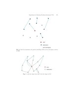
Microtubes can be made straight or curved (Fig. 7),
or they can be coiled (Fig. 8). Coiled tubes whose coils
are as small as 20 µm can be used, for example, as flex-
ible connectors or solenoid coils. For the latter applica-
tion, the coils could be of metal or of a high temperature
superconductor where liquid nitrogen flows through the
(a)
(b)
Figure 5. (a) Sapphire tube that has a silver liner. (b) Nickel tube
that has a silver liner.
Figure 6. Solid nickel structure that has oriented microchannels.
tube. Another application for coils is for force or pres-
sure measurement. No longer are we limited to quartz mi-
crosprings. Using microtube technology, the diameter and
wall thickness of the tube, the diameter of the coil, the
tube material, and the coil spacing can be very precisely
(a)
(b)
Figure 7. Examples of curved silver tubes: (a) single tube;
(b) multiple tubes.
P1: FCH/FYX P2: FCH/FYX QC: FCH/UKS T1: FCH
PB091-M-drv January 12, 2002 1:4
MICROTUBES 651
(a)
(b)
Figure 8. (a) Section of “large” coiled tube. (b) Open end of coiled tube.
controlled to give whatever spring constant is needed for
the specific application. In addition, these microcoils can
be made from a variety of smart materials and used as
actuators or sensors. For example, the length of a spring
made from Nitinol
® can easily be changed by applying
heat. It is also possible to wrap one or more coiled spring
tubes around a core tube (Fig. 9). Applications for this kind
of device range from a counterflow heat exchanger to a
screwdrive for micromachines. (For the screw application,
the wrapped coil cross section could be made rectangular.)
Like coiled spring tubes, bellows can be used as microin-
terconnects, sensors, and actuators and can be made in
practically any shape imaginable. Figure 10a shows a bel-
lows that has a circular cross section, and the bellows in
Fig. 10b has a square cross section and aligned bellows
segments. The bellows in Fig. 10c is square and has a
twist. A slightly more complex bellows shown in Fig. 10d
is a tapered-square camera bellows that has a sunshade
to demonstrate the unique capability of this technology. It
demonstrates the ability to control cross section and ax-
ial shape and to decrease and increase the cross-sectional
Figure 9. A coiled tube wrapped around a tube or fiber that can
be used as a heat exchanger or as a microscopic screwdrive.
dimension in the same device. Bellows fabricated by mi-
crotube technology can have a variety of shaped ends for
connections to systems for use, for example, as finned heat
exchangers, hydrauliccouplings forgas and liquid, or static
mixers for multiple fluids. The bellows in Fig. 10e has a
thicker transitional region and a dovetail on the end for
connection to a device machined on a silicon wafer. The fe-
male dovetail to mate with this bellows is a commercially
available trench design (68) on a silicon wafer that pro-
vides a way to attach the bellows to the wafer, which can be
pressurized by using proper sealing. (No other technology
available can join a fluidic coupling to a wafer for pressur-
ization to relatively high pressures.)
If one end of the bellows is sealed, an entirely new group
of applications becomes possible. For example, if a bellows
end is sealed, the bellows can be extended hydraulically
or pneumatically. In this configuration, a bellows could be
used as a positive displacement pump, a valve actuator, or
for micromanipulation. As a manipulator, a single bellows
could be used for linear motion, three bellows could be or-
thogonally placed for 3-D motion, or three bellows could
be attached at several places externally along their axes
(Fig. 11) and differentially pressurized to produce a bend-
ing motion. This bending motion would produce a microfin-
ger, andseveral of thesefingers would make up a hand. The
large forces and displacements possible by using this tech-
nique far surpass those currently possible by electrostatic
or piezoelectric means and fulfill the need expressed
by Wise and Najafi (18) when they stated that “In the
area of micro-actuators, we badly need drive mechanisms
capable of producing high force and high displacement
simultaneously.”
For most applications, it is necessary to interface mi-
crotubes and the macroworld. This is possible in a num-
ber of ways. For example, a tapering process can be used
in which the diameter is gradually decreased to micron di-
mensions. Alternatively, the tubes and the macroworld can
be interfacedby telescopingor numerous types of manifold-
ing schemes (Fig. 12). An example of a thin-walled 5-µm i.d.
tube telescoped to a 250-µm o.d. tube is shown in Fig. 13.
A tube of this type could be used as a micropitottube and, of
course, could be made more robust by thickening the walls.
P1: FCH/FYX P2: FCH/FYX QC: FCH/UKS T1: FCH
PB091-M-drv January 12, 2002 1:4
652 MICROTUBES
(a)
(b)
(c)
(d)
(e)
Figure 10. (a) A conventional round bellows. (b) A straight bellows that has a square cross section
(c) A square bellows that has a twist. (d) A tapered square camera bellows that has a sun shade to
demonstrate the versatility of the technique. (e) A round bellows that has a dovetail connector.
Although microtube technology has unique capabilities,
it should be obvious that no single technology can fill all of
the requirements imposed by diverse applications. Thus,
microtube technology cannot easily compete with other
technologies in certain applications. One of these involves
gas and liquid separation such as in chromatography. For
example, quartz tubing that can be extruded and drawn
in very long lengths is inexpensive and available in mi-
cron dimensions. However, note that even in areas such
as separation, there are niches for microtubes that in-
volve the composition of the tube material, the cross-
sectional shape, or the inner wall coating. For example,
Fig. 14 shows microtubes manifolded to a tubular frame
for a specific gas separation that requires microtubes
P1: FCH/FYX P2: FCH/FYX QC: FCH/UKS T1: FCH
PB091-M-drv January 12, 2002 1:4
MICROTUBES 653
P
1
= P
2
= P
3
P
1
P
2
P
3
(a)
P
1
P
2
P
3
P
1
> P
2
> P
3
(b)
Figure 11. Microtube bellows finger: (a) unpressurized; (b) pressurized.
of a specific composition, precise diameter, and wall
thickness.
Currently, these tubes have been made by a batch pro-
cess in the laboratory, but the technique is equally suited
to a continuous process which would be more efficient and
also much easier in some cases. Obviously, a continuous
process would reduce costs. For most materials, costs are
already rather low because, unlike some other processes,
expensive tooling is not required. For many materials such
as quartz, aluminum, and copper, the anticipated cost is
(a)
(b)
(c)
(d)
Figure 12. Different ways of transitioning microtubes to the real world: (a) taper, (b) telescope,
(c) bundle, and (d) manifold.
∼$0.01/cm for thin-walled tubes. For precious metals such
as gold or platinum, the cost would be significantly higher
due to the cost of raw materials.
Microtubes have almost universal application in ar-
eas as diverse as optics, electronics, medical technology,
and microelectromechanical devices. Specific applications
for microtubes are as diverse as chromatography, encap-
sulation, cross- and counterflow heat exchange, injectors,
micropipettes, dies, composite reinforcement, detectors,
micropore filters, hollow insulation, displays, sensors,
P1: FCH/FYX P2: FCH/FYX QC: FCH/UKS T1: FCH
PB091-M-drv January 12, 2002 1:4
654 MICROTUBES
(a)
(b)
Figure 13. (a) A thin-walled 5-µm i.d. tube telescoped to a 250-µm o.d. tube. (b) View of the small
open end of the telescope.
optical waveguides, flow control, pinpoint lubrication, mi-
crosponges, heat pipes, microprobes, and plumbing for mi-
cromotors and refrigerators. The technology works equally
well for high- and low-temperature materials and appears
feasible for all applications that have been conceived to
date. As can be seen, there are numerous types of devices
that have become possible as a result of microtube tech-
nology. One category of devices that is highlighted is that
based on surface tension and wettability.
MICROTUBE DEVICES BASED ON SURFACE TENSION
AND WETTABILITY
Now, there is great interest in developing microfluidic sys-
tems to decrease the size of current devices, increase their
speed and efficiency, and decrease their cost because mi-
crofluidic systems have the potential, for example, for dras-
tically decreasing the cost of certain health tests, allowing
implantable drug delivery systems, and very significantly
reducing the time needed to complete the Humane Genome
Project. Microtube technology based on surface tension and
wettability is unique in its capabilities and is truly an en-
abling technology in the microfluidic field.
Figure 14. Microtubes are manifolded to a tubular frame for gas
separation.
As miniaturization of mechanical, electrical, and fluidic
systems occurs, the role of physical and chemical effects
and parameters has to be reappraised. Some effects, such
as those due to gravity or ambient atmospheric pressure,
are relegated to minor roles or can even be disregarded
entirely as miniaturization progresses. Meanwhile, other
effects become elevated in importance or, in some cases,
actually become the dominating variables. This “downsiz-
ing reappraisal” is vital to successful miniaturization. In
a very real manner of speaking, new worlds are entered
into in which design considerations and forces that are
normally negligible in real-world applications become es-
sential to successful use and application of miniaturized
technology.
Surface tension and wettability are closely related phe-
nomena that are greatly elevated in importance as minia-
turization proceeds. Surface tension involves only the
strength of attraction of droplet molecules for one an-
other (cohesive forces), but wettability also includes the
strength of attraction of droplet molecules to molecules
of the wall material (adhesive forces). It is important
to realize that surface tension and wettability are usu-
ally not comparable in effect to normal physical forces at
macroscopic levels. For example, surface tension is usually
ignored when determining fluid flow through a pump or
tube. Its effect is many orders of magnitude smaller than
pressure drop caused by viscosity because the difference
in pressure P between the inside of a droplet and the
outside is given by the Young and Laplace equation of
capillary pressure (69,70):
P = 2γ/r. (1)
In this equal-radii form of the capillary pressure law
used for a spherical droplet, γ is surface tension and r
is droplet radius. The pressure inside the droplet can be
thought ofas causedby asurface “skin,” similar to a balloon
that holds air in. Instead of a thin membrane of rubber as
in the case of balloons, however, confining forces in surface
tension are caused by the affinity of molecules of droplet
material for one another. Because molecules are missing a
P1: FCH/FYX P2: FCH/FYX QC: FCH/UKS T1: FCH
PB091-M-drv January 12, 2002 1:4
MICROTUBES 655
binding partner looking outward on the surface of a drop,
they pull on their nearest neighbors.
Normally, droplet dimensions in most macroscopic ap-
plications are measured in thousands of microns. There-
fore, pressure differences due to surface tension are incon-
sequential andtypically measure far less than atmospheric
pressure. For comparison, pressure drops resulting from
viscous flow are typically of the order of magnitude of tens
of atmospheres. When r is of the order of microns, however,
pressure differences due to surface tension become enor-
mous and frequently surpass tens of atmospheres. This is
precisely the reason that fine aerosol droplets are so diffi-
cult to form. However, the formation of tiny droplets is not
specifically the focus of discussion here, but rather their
behavior in miniature voids, such as cavities, capillaries,
and channels that are shaped so that they partially confine
the droplet. The position of droplets withinsuch microvoids
is governed by the surface tension of the droplet fluid, the
wettability of the fluid with respect to microvoid walls con-
tacted during displacement, the geometric configuration of
the walls that confine the fluid droplets, and any pressure
external to the droplet. Microdevices fabricated from these
microvoids can be made to operate when wettabilities are
greater than or less than 90
◦
, but not exactly 90
◦
. They
can operate using either nonwetting or wetting fluids. The
difference between wetting and nonwetting fluids in capil-
laries can be explained by using Fig. 15.
In Fig. 15a, a nonwetting fluid droplet is forced into a
single microtube. An insertion pressure has to push the
nonwetting droplet inside the microtube because of the re-
pulsion between the droplet and the walls. Once it is inside,
however, no further pressure is necessary. In fact, any pres-
sure simply moves the nonwetting droplet along the micro-
tube at a velocity determined by the applied pressure and
the frictional forces between the droplet and the microtube
wall. Note that the nonwetting droplet becomes elongated
when it is constrained in the capillary and has a convex-
shaped interface along the axis of the capillary. In addition,
it can be seen that the radius of the nonwetting droplet is
now greater than the radius of the microdevice tube and
that the contact angle θ with the capillary surface is be-
tween 90
◦
and 180
◦
, which is the contact angle for a totally
nonwetting droplet. In contrast, the situation is very differ-
ent if the fluid totally wets the microtube surface, as seen
Droplet
radius
Non-wetting
droplet
P
ent
Tube
diameter
(a)
Press.
Droplet
radius
Wetting
droplet
Press.
(b)
Figure 15. Behavior of fluid droplets in capillaries: (a) nonwet-
ting droplet; ( b) wetting droplet.
in Fig. 15b. In this case, the fluid is sucked into the micro-
tube, and fluid flow is governed only by frictional forces.
This is the situation in normal macroscopic applications.
For wetting fluids, the ends of the droplets are concave be-
cause the walls of the microdevice are wet by the droplet
and attract the droplet molecules. The contact angle for
wetting fluids is between 0 and 90
◦
,0
◦
indicates a totally
wetting fluid. In this article, the term nonwetting refers
to a contact angle greater than 90
◦
, and the term wetting
means a contact angle less than 90
◦
.
The behavior of a microtube device that employs non-
wetting droplets is easily understood if one compares it to
the mercury intrusion method (71–73) of measuring the
pore-size distribution within porous solids. This technique
is based on the understanding that the pressure needed to
force a nonwetting fluid into a capillary or a pore in a solid
is given by the relationship proposed by Washburn (71):
P = 2γ cos θ/r (2)
where θ is the contact angle of the fluid with the material
under test, P is the external pressure applied to the non-
wetting fluid, and r is the radius of the capillary or pore
which, act is assumed for simplicity, is spherical and has
a constant diameter. This equation is valid for any fluid in
contact with a capillary or porous solid whose contact an-
gle is greater than 90
◦
. Once the external applied pressure
exceeds that needed to insert the nonwetting fluid into a
constant-diameter capillary or pore, the nonwetting fluid
flows into that particular diameter capillary or pore until
it fills it. Then, the volume of the intruded fluid is a direct
measure of that particular capillary’s or pore’s void volume.
If a smaller capillary or pore branches off the larger dia-
meter void, it remains unfilled until the insertion pressure
is raised sufficiently high that Eq. (2) is again satisfied,
and the process repeats itself.
In contrast to the mercury intrusion method of deter-
mining pore volume, instead of determining the pore vol-
ume, the emphasis in devices based on microtube tech-
nology is placed on the movement and the position of the
droplet in the confining voids. These droplets can be wet-
ting or nonwetting. As will be apparent later, a myriad of
smart microdevices are based on surface tension and wet-
tability.
Because these microdevices have no moving mechani-
cal parts, they are very reliable, can be used in both static
and dynamic applications, and are very rugged. They can
experience pressures or forces far beyond their normal op-
erating range and still return to theiroriginal accuracy and
precision. In addition, unlike technology built up on a sili-
con wafer, these microdevices can be made from practically
any material. Thus, high-temperature microdevices can
be fabricated by properly choosing the device and droplet
material.
Devices That Use the Interaction of Nonwetting Droplets
and Gases and Wetting Fluids
This group of devices uses the surface properties of materi-
als, primarily surface tension and wettability, as the prin-
cipal means of actuating and controlling motion by and
P1: FCH/FYX P2: FCH/FYX QC: FCH/UKS T1: FCH
PB091-M-drv January 12, 2002 1:4
656 MICROTUBES
(a)
Non-wetting droplet
Microtube
Wetting fluid
Intersection
of tubes
Non-wetting
droplet
(b)
Figure 16. Nonwetting droplet inserted into a microtube under
pressure. (a) Constant diameter tube. (b) Tube that has a transi-
tion to a smaller diameter.
within microtube devices. These devices, which have no
moving mechanical parts, can perform mechanical tasks
whose scale of motion is measured in microns.
These devices, similar to other microdevices based on
surface tension and wettability, are composed of various
sizes of nonwetting droplets inserted into microscopic voids
of various shapes and sizes. These voids can be in the form
of cavities, capillaries, and channels that are shaped so
that they partially confine the droplet. Gas or wetting fluid
is placed in the microcavities along with the nonwetting
fluid. During operation, the nonwetting droplets move in
response to fluid or gas pressure or vice versa. Specifically,
these nonwetting droplets may translate within a void of
the microtube device that is filled with the gas or wetting
fluid, translate from one void space to another, or rotate
in a fixed position. Microtube devices of this type can stop
fluid flow or act as a check valve, a flow restricter, a flow
regulator, or a gate, for example. The minimum dimension
of the voids in these devices typically ranges from about
20 nm to about 1000 µm.
In Fig. 16a, a non-wetting fluid droplet is forced through
a single microtube. An initial insertion pressure has to
push the nonwetting droplet inside the microtube. If the
diameter of the microtube in Fig. 16a decreases at a cer-
tain point to form a telescoping microtube (Fig. 16b), a
considerably higher pressure must be applied by a gas
or wetting fluid to squeeze the nonwetting drop into the
smaller section of the microtube. In contrast, if a wetting
fluid is employed instead ofa gas, as before, it is also sucked
into the smaller diameter section, completely filling all the
available space in the microcavity. By inserting an appro-
priately sized nonwetting droplet into a tapered microtube
or a microtube that has a transition to a smaller dimen-
sion that is filled by a second fluid that wets the tube walls,
all flow of the wetting fluid can be stopped by applying a
pressure that forces the nonwetting droplet to block the
Non-wetting
droplet
Bypass
tube
Bypass
tube
(a)
Non-wetting
droplet
Bypass
tube
Bypass
tube
(b)
Figure 17. Microtube check valve: (a) flow possible through by-
pass tubes; (b) flow is blocked.
entrance to the smaller section of the cavity. This is the
situation in Fig. 16b where the nonwetting droplet has
been forced to the intersection of the larger and smaller
microtube sections by the flowing gas or wetting fluid.
Figure 17a,b illustrates an extension of this concept. By
adding additional small-diameter bypass-flow paths to one
end of a doubly constricted tube, flow is possible only in
the direction of the end that has the added flow paths at-
tached to the cavity. Of course, these bypass tubes must be
properly sized to prevent nonwetting droplets from squeez-
ing into them. This microtube device in Fig. 17 acts as a
check valve and has no solid moving parts. This cannot
be achieved at the macroscopic level because forces that
arise from surface tensions of fluids are too small due to
the much larger geometries employed.
Figures 18 and 19 are further extensions of this same
concept. In Fig. 18, bypass tubes are left off the microtube
check valve and convert it to either a microtube flow limiter
(Fig. 18) or a microtube flow restricter (Fig. 19). In Fig. 18,
because the nonwetting droplet and the larger tube wall
form a seal, the only wetting fluid flow that can occur in
either direction when the nonwetting droplet travels back
and forth is equal to the volume of the larger tube section
minus the volume of the nonwetting droplet. In Fig. 19, the
diameter of the nonwetting droplet is now smaller than the
diameter of the larger microtube section but larger than
Non-wetting
droplet
Figure 18. Microtube flow limiter.
P1: FCH/FYX P2: FCH/FYX QC: FCH/UKS T1: FCH
PB091-M-drv January 12, 2002 1:4
MICROTUBES 657
Non-wetting droplet
Figure 19. Microtube flow restricter.
the diameter of the smaller microtube. Thus, flow can take
place around the nonwetting droplet. However, fluid flow
is not merely restricted, but is entirely stopped if there is
enough flow to push the drop to one end that blocks the
smaller tube.
Figure 20 illustrates a microtube pressure/flow regu-
lator. In this device, bypass tubes have openings or are
open along their entire lengths to a conically shaped tran-
sitional region placed between the larger and smaller dia-
meter tubes. Furthermore, the lengths of the joined bypass
tubes (now better described as bypass channels) up to the
conical transitional region can be varied. Increased pres-
sure or flow forces the nonwetting droplet farther into the
conical transitional region and exposes more flow channel
openings to wetting fluid. The result is increased flow of the
gas or wetting fluid as a function of pressure. By suitably
sizing the nonwetting droplet, properly orienting the de-
vice, correctly shaping the transitional cone, and precisely
positioning bypass channels, this device can also function
as a microtube pressure-relief valve; no flow occurs un-
til some predetermined pressure is exceeded. Then, flow
takes place as long as pressure is maintained. Note that
only two bypass flow channels are shown in Fig. 20. This
was done to simplify the drawing. Any convenient num-
ber, one or more, of channels can be employed. Finally, by
making bypass-flow channels vary in cross-sectional area,
uniformly increasing or decreasing flow can be produced
as a function of pressure.
In addition to a check valve, it is possible to use nonwet-
ting fluids to make a positive closure valve that has zero
dead space to control a gas or wetting fluid. Figure 21a,b
Wetting
fluid
Non-wetting
droplet
Conical
transition
Bypass
tube
Bypass
tube
Figure 20. Microtube flow or pressure regulator.
Non-wetting
fluid
Inlet
duct
Inlet fluid Outlet fluid
Fill
tube
Heater
End
bulb
Outlet
duct
Micro-channel
(a)
Inlet fluid
Heater
Non-wetting
fluid
Micro-channel
Inlet
duct
(b)
Figure 21. Positive closure microtube valve that has zero dead
space: (a) top view; (b) side view.
illustrates a microvalve composed of a fill tube joined to
an end bulb, where two microchannels are attached to the
fill tube. In this example, the nonwetting droplet controls
the flow of a wetting fluid or gas through a microchannel
whose thickness is less than that of the fill tube. In this mi-
crovalve, an inlet fluid flows through an inlet duct and then
into one of the microchannels. If the fill tube is not blocked
by the nonwetting droplet, the inlet fluid traverses the un-
blocked fill tube at the point where both microchannels at-
tach to it. Then, the fluid exits the microvalve through an
outlet duct as outlet fluid. In Figure 21a,b, the nonwetting
P1: FCH/FYX P2: FCH/FYX QC: FCH/UKS T1: FCH
PB091-M-drv January 12, 2002 1:4
658 MICROTUBES
A OUTB
0
1
0
1
01
0
1
1
0
0
1
Non-wetting
droplet 1
Non-wetting
droplet 2
A
B
Out
(a)
AB
Out
(b)
Figure 22. Microfluidic logic circuit that acts as comparator:
(a) output; (b) no output.
droplet is activated by a heater and only partially fills the
fill tube. Obviously, many other forms of activation are pos-
sible, and it is possible to assemble these microvalves in
parallel to control large flows of liquids or gases.
A final categoryof microfluidicdevices in which one fluid
controls another can be understood by the more complex
examples given in Fig. 22. These figures present microtube
devices that use surface tension and wettability in fluidic
logic circuits that are fully digital, not analog. The device
in Fig. 22 functions as a comparator; there is an output
only if the inputs are equal. Thus, if pressure is applied
to either branch A or B, the gate (nonwetting droplet 2)
closes, as in Fig. 22b, and no flow occurs (and no pressure
is transmitted) between branches C and D. If equal pres-
sure is applied to A and B or no pressure is applied to A
and B, the gate remains open as in Fig. 22a, and flow occurs
(and pressure is transmitted) between C and D. Nonwet-
ting droplet 1 is returned to the center position when-
ever pressure is removed because surface tension always
minimizes droplet surface area and a sphere has the low-
est surface area per unit volume of any object. Only at the
center position can it be a sphere, and unless placed under
unbalanced force by pressure from A or B, it remains at
the center. Numerous other types of logic circuits, such as
OR, NOR, AND, and NAND gates, can also be fabricated in
this manner. By combining a number of these logic compo-
nents in a suitable arrangement, digital operations can be
performed identically to those of electrical devices. Instead
of electricity being on or off in a circuit, pressure is applied
or not applied, and fluid flow does or does not occur.
Microdevices Based on the Positions and
Shapes of Nonwetting Droplets
In this group of microdevices, the basic principle of op-
eration is the movement or shape change of nonwetting
droplets in tubes, channels, or voids that have at least one
microscopic dimension. This movement on shape change
results from external or internal stimuli. The change in
droplet shape depends on the cavity shape and always
minimizes the surface free energy ofthe droplet. The cavity
that constrains the droplet in these devices can be sealed
or can have one or more openings. The shape of this cav-
ity determines the reaction of the droplet to a stimulus,
as well as the use of the microdevice, and the output that
can be obtained from it. Uses for these microdevices are as
diverse as sensors, detectors, shutters, and valves.
As just stated, microtube sensors based on surface ten-
sion and wettability are one type of device in this group.
Some ofthese sensorsrespond to one or more external stim-
uli such as pressure, temperature, and gravity or acceler-
ation by changes in the displacement or shape of liquid
interfaces contained within microtubes and/or microchan-
nels that have either fixed or variable axial geometries and
circular or noncircular cross-sectional profiles. Other sen-
sors respondto internal stimuli, such as achange in surface
tension of the liquid droplet or a change in the wettability
of the microdevice’s internal walls. Some of these sensors
can quantify the displacement or change in shape of the
constrained droplet that is results from external or inter-
nal forces acting on it.
An example of one of the simplest microdevices in this
group of devices is a microtube pressure sensor (Fig. 23)
that uses a nonwetting fluid in the form of a droplet. Fig-
ure 23a illustrates the position of the droplet when the
entrance pressure P
ent
is equal to the device pressure P
dev
.
Figure 23b illustrates the position of the droplet when the
entrance pressure is greater than the device pressure P
dev
,
and Fig. 23c illustrates the position of the droplet when
there is a much higher entrance pressure. This sensor
demonstrates the reaction of such a device to an outside
stimulus which in this case is an increase in externally ap-
plied pressure P
ent
. As can easily be seen, the shape of the
nonwetting droplet changes in reaction to increases in the
applied external pressure P
ent
. More precisely, increasing
the external pressure P
ent
, that acts through an entrance
microtube squeezes the droplet into ever smaller diameter
locations within a microcavity, which results in displacing
the nonwetting interface toward the smaller diameter end
of the device. For this type of sensor, this microcavity may
be tear shaped, circular, or have practically any shape, as
long as there is a change in at least one dimension and
this dimension is from 0.003–1000 µm. For simplicity, the
pressure on the smaller side of the microdevice P
dev
, which
P1: FCH/FYX P2: FCH/FYX QC: FCH/UKS T1: FCH
PB091-M-drv January 12, 2002 1:4
MICROTUBES 659
(a)
P
ent
P
dev
P
ent
= P
dev
P
ent
P
dev
P
ent
> P
dev
(b)
P
ent
P
dev
P
ent
>> P
dev
(c)
Figure 23. Microtube pressure sensor based on surface tension
and wettability.
opposes the external pressure P
ent
, is set at zero in this fig-
ure. P
dev
is most easily thought ofas a residual gas pressure
left over inside the device from the actual fabrication pro-
cess. It does not have to be zero, as shown later. The only
requirement for this type of sensor is that P
dev
be less than
P
ent
and that both pressures be smaller than the burst-
ing strength of the walls of the microtube pressure sensor.
It should be apparent from Fig. 23 that an overpressure of
the device will push the droplet further into the device tube
than designed for, but when the pressure is released, the
droplet will return to its equilibrium position. As long as
the walls of the device have not been damaged and main-
tain their original shape, the sensitivity and accuracy of
this device and the others that are described following will
be unaffected by overpressure.
The reaction of the droplet to external pressure is eas-
ily calculable from surface tension theory (the change in
radius of the smaller end of the droplet is inversely pro-
portional to applied the external pressure), but the ac-
tual decrease in radius and resulting displacement of the
nonwetting interface can be understood only intuitively or
observed visually by microscope, as presented in Fig. 23.
Figure 24 illustrates a modification of this microtube pres-
sure sensor based on surface tension/wettability which
enables nonvisual determination of the displaced inter-
face. This nonvisual response to the reaction (movement
or shape change) of the droplet interface caused by a stim-
ulus can take many forms. One of these is a change in
electrical resistance. A center contact, which has a mea-
surable electrical resistance, is inserted through the mi-
crotube device and establishes electrical contact with the
nonwetting droplet. This center contact can be a wire, tube,
Meter
Resistance wire
Droplet
Side contact
P
ent
P
dev
Figure 24. Microtube pressure sensor that has a resistance wire
continuous readout.
tape, or any other elongated geometry desired. A second or
side contact is likewise placed in a position to make elec-
trical contact with the conductive droplet, but not make
direct contact with the center contact. These two contacts
are then connected to an apparatus that measures resis-
tance. If the nonwetting droplet material composition has
been selected so that it is electrically conductive as well as
nonwetting, any displacement of the nonwetting interface
that reduces the length of the center contact not touching
the droplet thereby results in reducing the center contact’s
resistance measured by the resistance measuring appara-
tus. To maximize this effect, the center contact should have
a very high resistance per unit length compared to the side
contact, the actual droplet itself, and compared to the re-
mainder of the circuit that connects both contacts to the
resistance measuring apparatus.
As stated previously, the opposing pressure P
dev
need
not be zero. It has been set at zero thus far for simplicity.
For this type of sensor, it merely needs to be less than the
externally applied pressure P
ent
; otherwise, thenonwetting
droplet could be expelled from the microtube pressure
sensor.
Note here that the devices shown schematically can
measure a variety of external or internal stimuli. The pres-
sure sensor in Fig. 24, for example, could also measure ac-
celeration and oscillation along the device axis as well as
rotation and temperature, which affect both the thermal
expansion and the surface tension of the droplet. If another
center contact is also placed in the device on the end op-
posite the present center contact, the device can measure
acceleration in two directions. In addition, it should be ap-
parent that to measure parameters such as temperature,
rotation, acceleration, or oscillation, it is not even neces-
sary for the entrance tube and the device tube to be open
to the atmosphere. Thus, to measure these external stim-
uli or some internal stimulus, a totally sealed cavity would
function as well as the open pressure sensor in Fig. 24.
For simplicity, only pressure sensors are shown sche-
matically, and it should be understood that the devices
work equally well in reaction to many other stimuli. A
partial list that includes vibration, acceleration, rotation,
temperature, electromagnetic fields, andionizing radiation
demonstrates the broad scope of this sensor technology.
When a wetting droplet is employed in place of a non-
wetting droplet, insteadof needing P
ent
to reach some value
given by Eq. (2) to force the droplet into the microtube, it
goes in automatically. This behavior is often referred to as
“wicking.” In contrast to the nonwetting droplet, no pres-
sure is needed to get the drop into the tube. The fact that
wetting dropletsbehavesimilarly tononwetting droplets in
P1: FCH/FYX P2: FCH/FYX QC: FCH/UKS T1: FCH
PB091-M-drv January 12, 2002 1:4
660 MICROTUBES
Non-wetting interface
P
ent
P
dev
Meter
(a)
Interface
P
ent
P
dev
Meter
(b)
Figure 25. Microtube pressure sensor that has a “Yes-No”
straight port.
some respects means that microdevice sensors can employ
either wetting or nonwetting fluids as the droplet mate-
rial and still serve the same function. For microtube pres-
sure sensors, this would require switching the side of the
droplet that actually “feels” the applied pressure. Microde-
vices thatsense other stimuli would also need similarkinds
of modification. These would be specific for the actual sens-
ing application.
Figure 25a,b illustrates the relationship between the
radius of curvature of the small end of the drop and the
various pressures involved for a microtube pressure sensor
that has a digital type of response; this will hereafter be
referred to as a “Yes-No” response. In Fig. 25a, the applied
pressure P
ent
is not sufficient, compared to P
dev
, to force
the nonwetting droplet into the straight port. Therefore,
the continuity apparatus registers an open circuit, or “No”
response. In Fig. 25b, the applied pressure P
ent
is sufficient
to force entry of the nonwetting droplet into the straight
port. Once the droplet has entered the straight port, it
completely fills it, and the continuity apparatus registers a
closed circuit, or “Yes” response. As mentioned previously,
this same kind of “Yes-No” response can be duplicated
by using wetting fluids. However, because a wetting fluid
would spontaneously wick into the smaller diameter tube,
the only difference would be that now an applied pressure
of sufficient magnitude would need to be directed to P
dev
to expel the wetting droplet from that same straight tube.
Therefore, for a wetting fluid, the continuity apparatus
would work in reverse to the “Yes-No” response for a non-
wetting droplet. In this case, P
dev
must be greater than P
ent
,
and therefore, an open circuit signifies “Yes,” and a closed
circuit signifies “No.” However, because a wetting droplet
adheres to the microdevice walls, including the straight
port, fluid remaining on these surfaces might compromise
the accuracy of the continuity apparatus. Therefore, it
is preferable to use nonwetting droplets in this kind of
sensor. This same logic applies to most microdevices based
on surface tension and wettability, and so in the discussion
that follows, only nonwetting behavior is illustrated.
There are obviously many other means for measur-
ing displacement of a nonwetting droplet. Other basic
electrical parametersthat can be employed are capacitance
and inductance. Note here that for all of the aforemen-
tioned techniques for measuring displacement of a nonwet-
ting dropletby using electricalmeans,the electricalproper-
ties of the nonwetting droplet must, of course, be suitable
for the measurement technique employed. For some ap-
plications, the resistance of the nonwetting droplet must
be sufficiently low to permit measuring the resistivity of
the center contact accurately enough for the application,
at hand. For other applications, the conductivity must be
high enough to enable measuring capacitance accurately.
For certain applications, permeability must be sufficiently
different between the nonwetting droplet and its surround-
ing medium in the microdevice to allow measuring induc-
tance accurately enough to satisfy the demands of the de-
sired application. These electrical property requirements
are most likely to be different, depending on the measuring
technique employed and the particular application being
developed. Note that it is also possible to combine two or
more readout techniques in a single device.
For either multirange or redundancy-driven applica-
tions, a great deal of variation is possible. These varia-
tions are in the form of identical or different devices, cavity,
and/or channel or tube configurations, as well as identical
or different types of readouts. Many different types of de-
vice channel or tube configurations are possible that will
give either linear or nonlinear responses, as well as analog
or digital responses to the stimuli being sensed. For ex-
ample, a gradual taper would produce a linear response,
whereas a very rapid taper would give a nonlinear re-
sponse. In another example, a device such as that shown in
Fig. 25 could be modified with a tapered section to follow
the constant dimension tube. This would result in a dig-
ital response followed by an analog response. In addition
to these differences in individual sensors, multiple sensors
could all be used together simultaneously or switched on
or off as needed.
As mentioned previously, the presence or absence of
nonwetting material in a straight tube (Fig. 25) enables
the pressure sensor or other microdevice that derives its
capabilities from surface properties of materials to func-
tion in a digital or a “Yes-No” mode of response. Figure 26
illustrates anothervery simplekind of“Yes-No” readout re-
sponse for a pressure sensor that does not have a straight
tube. Now, the center contact in Fig. 24 has been trun-
cated, so that it does not make contact with the non-
wetting droplet for low values of the pressure difference
between P
ent
and P
dev
. This lack of contact, or gap, is shown
in Fig. 26. The truncated center contact makes contact
only with the nonwetting droplet once a predetermined
Side contact
P
ent
P
dev
Central contact
Meter
Figure 26. Microtube pressure sensor that has a “Yes-No” central
contact.
P1: FCH/FYX P2: FCH/FYX QC: FCH/UKS T1: FCH
PB091-M-drv January 12, 2002 1:4
MICROTUBES 661
P
dev
P
ent
Side contact
Positioner
Droplet interface
Central contact
Meter
Figure 27. Microtube pressure sensor that has a variable “Yes-
No” central contact.
pressure difference exists (P
ent
greater than P
dev
). Once
this occurs, the continuity meter signals that contact has
been made, and the desired “Yes-No” readout response is
provided. Once sufficient pressure difference has been es-
tablished, the truncated center contact can then function
as a center resistance contact, center contact, some other
kind of readout implement, or some combination thereof.
The truncated center contact should not move relative to
the microdevice walls in this simple form of “Yes-No” read-
out microdevice. It should be apparent that devices of this
type that have a truncated center contact can also serve as
an electrical switch, based on surface tension and wettabi-
lity, that can be made to operate independently of gravity,
can be impervious to radiation, and can be activated by
numerous stimuli.
A more sophisticated “Yes-No” readout microdevice
pressure sensor is illustrated in Fig. 27. Now the truncated
center contact is attached to a positioner, which, in turn, is
attached to a positioner holder, which is itself held firmly
in place relative to the actual microdevice walls. In Fig. 27,
the positioner holder is shown attached to the microdevice
walls. The positioner isany type of device that can move the
truncated center contact relative to the microdevice walls
in a predetermined fashion. Examples of such positioning
devices are numerous. They can be the type where the op-
erator sets the gap and thereby controls the device’s sensi-
tivity, such as a pressurized microbellows and a piezoelec-
tric crystal. Alternatively, the positioning device can be the
type that is influenced by its environment, such as those
made from photostrictive, chemostrictive, electrostrictive,
or magnetostrictive materials, which change length due to
light, a chemical environment, or an electric or magnetic
field. In these types of “smart”materials, the positioner
can be controlled in real time by its environment, and
thus the device can respond to two stimuli simultaneously.
Moreover, using any such positioning devices, the gap can
be changed by a feedback circuit. By altering the size of the
gap either before or during actual operation of the microde-
vice, the amount of pressure difference needed between P
ent
and P
dev
to establish contact and thereby evoke the “Yes-
No” readout response or continuity, as measured by the
continuity apparatus, can be changed. Thus, the sensitivity
of this device can be changed by an operator, by its environ-
ment, or by a feedback circuit. As before, once continuity
has been established for the simple “Yes-No” readout re-
sponse microdevice of Fig. 27, the truncated center contact
Droplet interface
P
ent
Light
Optical fiber
Figure 28. Microtube pressure sensor that has an interferometer
readout.
can be used for other kinds of readout purposes. For exam-
ple, the continuity apparatus can be modified to function
as the resistance measuring apparatus shown in Fig. 24.
If this is done, both digital and analog readout responses
can be garnered from the same sensor. More than one cen-
ter contact of different lengths and/or more than one side
contact can also be employed in Fig. 27, thereby providing
multiple digital responses from one device.
Note that the sensing techniques mentioned thus far
have all been relatively simple and have employed prin-
ciples of physics that are intuitively easy to understand:
changes in resistance, capacitance, or inductance. Another
simple technique for detecting the position of a droplet in-
terface is using an electromagnetic beam impinging on a
detector that is blocked by the advancing surface of the
droplet. This type of arrangement can basically give only
a “Yes”-“No” response. Two other techniques that can also
be employed to monitor displacement of the nonwetting
droplet interface are optical interference and electron tun-
neling. These techniques are capable of much higher lev-
els of resolution of the nonwetting droplets’ displacement,
which results in greater levels of sensitivity.
Figure 28 illustrates the readout technique that em-
ploys optical interference. The only additional require-
ment that must be imposed to use this technique is that
the nonwetting droplet must reflect at least some of the
electromagnetic radiation input through the fiber-optics
input/output cable back through the same cable. If these
conditions are met, an interference pattern can then be
generated between the incoming and outgoing rays of ra-
diation thatcan bedetected bya suitableapparatus located
at the opposite end of the fiber-optics input/output cable.
This interference pattern will be highly dependent on the
position of the internal interface of the nonwetting droplet,
as well as on the wavelength of radiation employed. There-
fore, it is an extremely accurate technique for monitoring
any displacement of that interface.
Figure 29 illustrates the readout technique for elec-
tron tunneling. There are two primary differences between
this readout technique and the previous readout tech-
nique that employs a truncated center contact, as illus-
trated in Fig. 27. In this apparatus, the truncated center
contact is replaced by a very sharp needle-shaped elec-
trode. In addition, the continuity apparatus is replaced by
a much more sensitive electron tunneling current detec-
tor that can measure the tiny electrical currents gener-
ated when the needle-shaped electrode moves very close
to the internal interface and creates gaps of the order of
atomic dimensions. As in optical interference, tunneling
current measurements are many times more sensitive to
P1: FCH/FYX P2: FCH/FYX QC: FCH/UKS T1: FCH
PB091-M-drv January 12, 2002 1:4
662 MICROTUBES
Meter
Droplet interface
Tunneling tip
(Tunneling current)
Figure 29. Microtube pressure sensor that has a tunneling cur-
rent readout.
displacements of the internal interface than simpler read-
out techniques discussed initially. Obviously, any other de-
tecting technique used in scanning probe microscopy, such
as atomic force, magnetic force, or capacitance, can be used
in place of the needle-shaped electrode and the current-
detection circuit. In addition, the sensitivity of these de-
vices, as in the device in Fig. 27, can be changed by varying
the gap between the tip and the droplet.
At this point, it is well worth mentioning again that the
movement of a droplet in a microscopic tube, channel, or
void and the process of remote measurement of displace-
ments of the internal interface itself is of critical signifi-
cance to the devices shown, not the actual kind of remote
measurement technique employed. Whatever technique is
employed affects only the accuracy of the remote readout.
Thus, regardless of the measurement technique, displace-
ments of the internal interface in reaction to external stim-
ulus will be the same and will depend only on the surface
tension and wettability of the sensor components and on
sensor geometry.
Until now, it has been tacitly assumed that motion of
the internal interface during any remote readout of its
displacement is negligible. This is not necessarily so. Any
measurement of the position of the internal interface will
take some finite amount of time. If there is motion of the in-
ternal interface during this finite measurement time, the
position of the internal interface will be some sort of av-
erage readout. If this is acceptable to the designer of the
microdevice, all is well. If it is not, either the method of
remote readout or the level of precision of the analytical
instruments employed must be changed to increase the
speed of readout to the degree required. Once this has
been done, microdevices based on surface tension and wet-
tability that have remote readout capabilities can func-
tion either as static or dynamic analytical detectors or
sensors.
Until now, it has also been assumed that the shaped
or tapered microtubes or microchannels within which
droplets move or flow underthe influence of surface tension
and wettability and some external forcing agent such as
pressure or acceleration, had circular cross sections. This
does not have to be so. Figure 30a, b illustrates flow of
an elongated nonwetting mercury droplet constrained on
P
P
Non-wetting droplet
Square capillary wall
(a)
Non-wetting droplet
Open corner
Open corner
(b)
Figure 30. Nonwetting droplet in square channel: (a) side view;
(b) end view.
four sides by walls that form a square cross section. For
mercury and other high contact angle liquids whose con-
tact angles are greater than 135
◦
, there will always be open
corners in a channel that has right-angle corners. These
corners remain unfilled because infinite internal pressure
would be required in these high contact angle liquids, the
result of setting r equal to zero in the relationship given
in Eq. (2), to fill in all corners completely. This can never
be true for two reasons. First, there is no such entity as
infinitely high pressure. Second, in Fig. 30a,b, bypass flow
of externally applied pressure P
ent
will occur through all
open corners, thereby reducing the actual pressure applied
to the nonwetting droplet. An analogous situation occurs
when a child shoots an irregularly shaped pea through a
circular straw. Even though gaps equivalent to the open
corners in Fig. 30a,b exist around the pea, the child can
still expel the pea from the straw simply by blowing hard
enough, thereby producing a sufficiently effective pres-
sure on the pea to accomplish the purpose. This is exactly
the situation that exists for flow of nonwetting droplets
in noncircular microtubes or microchannels. Therefore, all
previous arguments for remote sensing of droplet inter-
faces in circular cross-sectioned microtubes or microchan-
nels apply equally well to remote sensing of droplet inter-
faces in microtubes, microchannels, or voids that have any
type of noncircular profile. Moreover, noncircular micro-
tubes or microchannels can certainly be used in conjunc-
tion with circular microtubes or microchannels in the same
microdevice. In fact, there is very good reason to do so.
Noncircular microtubes or microchannels can be fabricated
relatively easily by using techniques such as photolithog-
raphy and LIGA on a surface. This is currently done on
silicon wafers by a sequence of deposition and/or etching
techniques in a number of different ways, two of which will
be given. A noncircular channel can be formed, for exam-
ple, by etching the channel in the surface and then covering
the channel by sealing a glass plate over it. Alternatively,
for example, the noncircular channel can be formed by
etching a channel in the surface and then filling it with
P1: FCH/FYX P2: FCH/FYX QC: FCH/UKS T1: FCH
PB091-M-drv January 12, 2002 1:4
MICROTUBES 663
a sacrificial material. Another material is deposited over
the filled channel and then the sacrificial material is re-
moved to leave a microchannel. However, no matter how
the noncircular channel is formed in the surface, a bypass
flow of gases occurs through its open corners, as illustrated
in Fig. 30b, if the liquid has a high contact angle. As just
mentioned, this makes it difficult to apply pressure accu-
rately and reproducibly to some nonwetting droplets con-
tained within such microtubes or microchannels. This is
not true for circular microtubes or microchannels. Thus,
the presence of small circular microtubes or microchan-
nels at appropriate positions in any device fabricated from
noncircular microtubes or microchannels will allow either
gases or wetting fluids to apply hydrostatic pressure to
microdevices that contain nonwetting droplets at 100% ef-
ficiency. The reverse is also true. A circular cross section in
the device will also allow the nonwetting droplet to apply
force to the gas or wetting fluid at 100% efficiency. This also
means that it is possible to have wetting and nonwetting
fluids in the same microdevice. Finally, regardless of the
cross-sectional shape of the microtubes, microchannels, or
voids, all wetting fluids will have 100% efficiency.
It is extremely important to realize that the previous
discussion also illustrates that an elongated non-wetting
droplet confined within a microtube or microchannel that
has, for the sake of illustration, square walls can serve
purposes other than remote sensing. For example, it can be
used to act as a shutter in optical applications, where the
presence or absence of the droplet controls whether or not
light or other electromagnetic radiation is allowed to pass
through the square microchannel walls. In this instance,
the nonwetting droplets function in much the same fashion
as a window blind by controlling whether or not light is let
through a window depending on whether or not the blind is
up or down. It could also control particle beams in a similar
manner.
Figure 31 illustrates a much more familiar looking
shutter mechanism that could very easily function iden-
tically to traditional mechanical shutters. An end bulb is
connected to a fill tube, and both are filled by a nonwetting
liquid, which is called the working fluid and is opaque
for the particular application. A rectangular void is also
connected to the fill tube, but its thickness is less than
the diameter of the fill tube. (The thickness of the void
in this figure is exaggerated for clarity.) The shutter that
has constant void thickness is illustrated in the open
configuration in Fig. 31a,b, where the incident radiation
or particle beam passes through the shutter, and is closed
in Fig. 31c,d where the incident beam or radiation is
blocked by the shutter. The void width and void length
can be much greater than the void thickness and only
one void dimension has to be macroscopic to carry out a
shutter’s function. This illustrates an extremely important
point: although all of the dimensions of a device can be
microscopic, only one dimension of a device must be in
the range where surface tension and wettability become
dominant factors in the device’s reaction to internal or
external stimuli to consider the device a microdevice. The
rectangular shutter of constant void thickness illustrated
in Figure 31 must be considered a microdevice because of
the microscopic dimensions of its thickness, even though
Light
Light
End bulb
Working
fluid
Fill tube
Thickness
Void
Fluid interface
(a)
Non-wetting interface
Heater
Length
Width
End bulb
Fill tube
Void
Working
fluid
(b)
Light
Working fluid
interface
(c)
Working fluid
interface
(d)
Figure 31. Macroscopic microtube rectangular shutter: (a) side
view of open shutter; (b) top view of open shutter; (c) side view of
closed shutter; (d) top view of closed shutter.
it can have very macroscopic dimensions for one or more
of its other features. This is true for all microdevices based
on surface tension and wettability. In this example, the
method of actuation of the rectangular shutter shown in
Fig. 31 is derived by an externally generated electrical cur-
rent input through a heater contained within the working
fluid. As the working fluid expands due to this heat input,
P1: FCH/FYX P2: FCH/FYX QC: FCH/UKS T1: FCH
PB091-M-drv January 12, 2002 1:4
664 MICROTUBES
any gas bubbles or other gas-filled voids contained within
the working fluid become compressed, thereby raising
the internal pressure P
int
within the working fluid. This
thrusts the internal interface farther and farther into the
rectangular void. At some point, the radius will decrease
sufficiently, so that the internal interface will shoot across
the void length, providing that the volume of compressed
gas-filled voids is much larger than the volume of the
shutter. This will close the shutter in the same fashion
as the “Yes-No” devices described earlier in Fig. 25. If gas
bubbles or other gas-filled voids are not present in the
working fluid, then the heat input will not cause a “Yes-No”
type of reaction, but rather will enable the shutter to close
more gradually. In this way, a partially closed shutter can
be maintained by controlling the heat input appropriately.
The gradual closing capability can be obtained for a
pressure-activated shutter by employing a void thickness
that has a decreasing taper. A different tapered end is
shown at the end of the rectangular void where the work-
ing fluid stops in the closed position. This is to minimize
the water hammer effect and does not have to be present
for the shutter to work. Of course, external pressure or
some other external stimuli as well as an internal stimuli
could also be used in place of the heater, and the shutter
would still function. If pressure were employed, it would
then be a pressure sensor that has some macroscopic
dimensions that would be very easy to observe. Filling of
the void would signify that a certain pressure had been
reached. Obviously, there are numerous other applications
of this technology but only two others will be mentioned.
One involves using a reflective nonwetting fluid, so that a
mirror results when the void space is filled, and the second
application encompasses a much larger microscopic void
area. If the void space is made as large in area as a window
pane, solar energy acting on the reservoir could be used
to force liquid into a void of microscopic dimensions in the
window pane and thus block sunlight from going through
the window if an opaque nonwetting liquid is employed.
The void shown in Fig. 31 has constant thickness and
is rectangular. Neither parameter is necessary. Figure 32
illustrates a circular shutter, which has a straight top face
and a curved bottom face that make up the void. Now, de-
pending on the amount of expansion of the working fluid
caused by electric power supplied to the heater, the shutter
can be completely open when all of the working fluid is con-
tained within the outside bulb, completely shut and have
no circular gap in the center at all, or anywhere in between,
as Fig. 32 illustrates. Certainly, both the top face and bot-
tom face can be curved or straight, and virtually any shut-
ter geometry can be employed. Likewise, actuating tech-
niques other than heat input to the working fluid by an
internal heater can be used. External heat input by radia-
tion orconduction orchanges inthe internalpressure ofthe
working fluid by any other means can be used to achieve
the same resulting shutter behavior.
As mentioned earlier, surface tension and wettability
govern the position of droplets within microdevices. Thus,
in addition to the external stimuli already mentioned, any
external stimuli that changes either the surface tension
of the droplet or the wettability of the surface can be de-
tected by a suitably designedmicrodevice sensor. Some, but
(a)
Heater
Outside
bulb
Working
fluid
interface
Circular
gap
Light
Top
face
Bottom
face
Light
Outside
bulb
Heater
Interface
Working
fluid
(b)
Figure 32. Circular shutter or iris: (a) side view; (b) top view.
not all, such stimuli include the following: temperature,
magnetic field, electrical field, rotation, radiation, and
beams of particles.
Until now,all ofthe microdevice sensors illustrated have
been designedto respondto external stimuli. This is not the
only mechanism for displacing microdevice droplets. Any
compositional change that occurs within droplets them-
selves or on the walls of microdevices can also change sur-
face tension or wettability. These changes can be either
reversible or irreversible and can be caused by a gas or wet-
ting fluid in the device along with the nonwetting droplet.
In addition, the surface tension of the droplet increases
as both the temperature and rotation increase. If these
or any other internally induced change in a microdevice’s
surface tension or wettability occurs, it can be detected and
monitored remotely using any of the techniques described
previously. Obviously, these internally induced changes in
a microdevice’s surface tension or wettability can also be
used to move the droplet(s) to perform work.
In addition, no actual dimensions of either microtubes
or microchannels have yet been discussed. Assuming a
nonwetting fluid such as mercury, which has a surface ten-
sion at room temperature of approximately 470 dynes/cm
and a contact angle on glass microdevice walls of roughly
140
◦
, one can calculate the following droplet radii for the
indicated internalpressures using Laplace’s equation mod-
ified to include the effect of wettability (Table 1):
In this section, we have shown that the flow of droplets
within microtubes and microchannels that is controlled by
surface tension and wettability can be used to sense, quali-
tatively and quantitatively, any environmental factor that
acts on a droplet or affects either its surface tension or
P1: FCH/FYX P2: FCH/FYX QC: FCH/UKS T1: FCH
PB091-M-drv January 12, 2002 1:4
MICROTUBES 665
Table 1. Calculation of Droplet Radii
r
dev
(µm) P
int
(lb/in
2
) P
int
(kPa)
950 0.1 0.69
95 1.0 6.89
9.5 10 68.9
0.95 100 689
0.095 1,000 6890
0.003 100,000 689,000
wettability, or both. This sensing can be performed
remotely bya varietyof techniques. It has also been demon-
strated that wetting droplets can sometimes be used with
only minor device modifications. Static as well as dynamic
remote sensing can be performed, and microtubes or mi-
crochannels that have circular or noncircular cross sec-
tions and variable axial geometries can be employed either
individually or together. The reaction of these devices to
any stimuli can be tailored by the device geometry and the
method of sensing and result in linear and nonlinear ana-
log output, as well as digital output. The use of this tech-
nique in nonsensing applications that perform mechani-
cal functions was also demonstrated. Finally, whenever at
least one microdevice dimension lies between 1000 µm and
0.003 µm, it has been shown that it can perform all of the
various tasks that have been discussed.
Nonwetting Droplets That Perform Work
The preceding discussion has indicated that the movement
of nonwetting droplets within microtubes or microchan-
nels can be used for sensing and controlling fluids. In ad-
dition, microscopic nonwetting droplets can be used for
mechanical control and manipulation within microdevices,
including tasks such as position control, moving objects,
deforming objects, pumping fluids, circulating fluids, and
controlling their flow. Obviously, complex machines anden-
gines can be produced by properly joining actuator and
pumping elements.
An application of a microscopic nonwetting droplet for
low friction position control is a microtube liquid bearing
shown in Fig. 33. Referring to Fig. 33a, for example, the
bearing assembly is a microtube that has one or more cir-
cular channels on its circumference that actually join the
microtube’s interior void space in a narrow ring-shaped
opening. A center rod only slightly smaller in diameter
than thebearing assembly issupported bynonwetting fluid
that fills the circular channels. This fluid cannot leak out
around the center rod if the gap is small enough because
too much pressure (Table 1) is required to form the droplet
of smaller radius that would be able to leak. Therefore, the
center rod is free to either rotate or translate axially within
the bearing assembly. It is called an external bearing be-
cause of this outside configuration. The only restraining
forces involved are frictional forces between the center rod
and the non-wetting fluid.
Figure 33b illustrates a reciprocal situation called a
microtube internal bearing. A straight walled microtube
is used. A central rod has at least one groove about the
circumference, and the nonwetting fluid fills this groove,
which allows both rotational and translational motion.
(a)
Center rod
Circular channel
Non-wetting
fluid
Circular channel
Non-wetting
fluid
Central rod
(b)
(c)
Circular channels
Non-wetting
fluid
Central rod
Figure 33. Shaft supported by nonwetting fluidic bearings:
(a) rotating and translating outer bearing; (b) rotating and trans-
lating inner bearing; (c) inner/outer bearing that rotates but does
not translate.
Figure 33c is a mixed combination of internal and external
microtube liquid-bearing locations. In this configuration,
however, only rotational motion is easily achieved. For
translation to occur, shearing of a wetting droplet must
take place. Although this is not as difficult as forming a
small-radius annular droplet, it still involves generating
new droplet surface area and therefore requires more force
to produce translation than for either the purely internal
or purely external bearings.
Figure 34 illustrates a microtube liquid bearing that
will not allow significant translational motion. It is a
Non-wetting
bearings
Figure 34. Thrust bearing that incorporates four nonwetting
fluid bearings.
P1: FCH/FYX P2: FCH/FYX QC: FCH/UKS T1: FCH
PB091-M-drv January 12, 2002 1:4
666 MICROTUBES
Droplet
radius
Piston
Gap
Non-wetting
droplet
Figure 35. Piston actuated by nonwetting fluid.
thrust bearing that uses four separate microtube liquid
bearings in an external configuration. As before, an in-
ternal or mixed configuration is also possible, and ad-
ditional microtube liquid bearings that use surface ten-
sion/wettability effects can be employed.
Figure 35 illustrates how a nonwetting droplet can be
employed as an actuator; its motion down a microchannel
or microtube is used to move a loosely fitting piston. It is
important to note that as long as the droplet does not wet
the piston and walls, none of the droplet will squeeze by
the piston if the clearance is less than the radius of the
nonwetting droplet. The nonwetting droplet is deliberately
shown only in part in Fig. 35 to demonstrate that the
actual mechanism, external stimuli, or internal stimuli,
or wetting fluid, that causes it to push on the piston
is unimportant. Its ability to function to transmit force
mechanically and thereby perform work is all that matters.
CONCLUSIONS
Microtubes appear to have almost universal application in
areas as diverse as optics, electronics, medical technology,
and microelectromechanical devices. Specific applications
for microtubes are as wide ranging as chromatography, en-
capsulation, cross- and counterflow heat exchange, injec-
tors, micropipettes, dies, composite reinforcement, detec-
tors, micropore filters, hollow insulation, displays, sensors,
optical waveguides, flow control, pinpoint lubrication, mi-
crosponges, heat pipes, microprobes, and plumbing for mi-
cromotors and refrigerators. The technology works equally
well for high- and low-temperature materials and appears
feasible for all applications that have been conceived to
date.
The advantage of microtube technology is that tubes
can be fabricated inexpensively from practically any mate-
rial in a variety of cross-sectional and axial shapes in very
precise diameters, compositions, and wall thicknesses of
orders of magnitude smaller than is now possible. In con-
trast to the other micro- and nanotube technologies cur-
rently being developed, microtubes can be made from a
greater range of materials in a greater range of lengths and
diameters and far greater control over the cross-sectional
shape. These tubes will provide the opportunity to minia-
turize (even to nanoscale dimensions) numerous products
and devices that currently exist, as well as allowing the
fabrication of innovative new products that have to date
been impossible to produce.
Space only allowed presenting one application of micro-
tube technology to new innovative products in greater de-
tail. This one application comprised those devices that are
based on surface tension and wettability. The few devices
that were shown as examples demonstrated the breadth of
this technology only in one field. The application of micro-
tube technology to other fields is considered equally rich
and limited only by a designer’s imagination.
ACKNOWLEDGMENTS
The invaluable help provided by Hong Phan in fabrica-
tion, Marietta Fernandez in microscopy, and Tom Duffey
in artwork is greatly appreciated. Financial support from
Dr. Alex Pechenik of the Chemistry and Materials Science
Directorate, Air Force Office of Scientific Research was re-
sponsible for much of this work.
BIBLIOGRAPHY
1. G. Stix, Sci. Am. 267: 106–117 (1992).
2. W. Menz, W. Bacher, M. Harmening, and A. Michel, 1990 Int.
Workshop on Micro Electro Mechanical Syst.(MEMS 90), 1990,
pp. 69–75.
3. C.G. Keller and R.T. Howe, Transducers 95, Stockholm,
Sweden, 1995, pp. 376–381.
4. W. Hofmann, C.S. Lee, and N.C. MacDonald, Sensors and
Materials 10: 337–350 (1998).
5. S.Y. Chou, P.R. Krauss, and P.J. Renstrom, Science 272:85–87
(1996).
6. S. Weiss, Photonics Spectra 108 (Oct. 1995).
7. M. Mullenborn, H. Dirac, and J.W. Peterson, Appl. Phys. Lett.
66: 3001–3003 (1995).
8. D.Y. Kim, S.K. Tripathy. L. Li, and J. Kumar, Appl. Phys. Lett.
66: 1166–1168 (1995).
9. K.H. Schlereth and H. Bottner, J. Vac. Soc. Technol., B10: 114–
117 (1992)I.
10. B.D. Terris, H.J. Mamin, M.E. Best, J.A. Logan, D. Rugar, and
S.A. Rishton, Appl. Phys. Lett. 69: 4262–4264 (1996).
11. Y. Xia and G.M. Whiteside, Angew. Chem. Int. Ed. 37: 550–575
(1998).
12. M. Ishibashi, S. Heike, H. Kajayama, Y. Wada, and
T. Hashizume, J. Surf. Anal. 4: 324–327 (1998).
13. H.J. Mamin and D. Rugar, Appl. Phys. Lett. 61: 1003–1005
(1992).
14. W. Li, A. Virtanen, and R.M. Penner, J. Phys. Chem. 96:6529–
6532 (1992).
15. E.E. Ehrichs and A.L. de Lozanne, Nanostructured Physics
and Fabrication. Academic Press, NY, 1989, pp. 441–445.
16. J.C. Harley, M.S. Thesis, University of Pennsylvania, 1991.
17. D.J. Harrison, K. Fluri, K. Seiler, Z. Fan, C.S. Effenhauser, and
A. Manz, Science 261: 895–897 (1993).
18. K.D. Wise and K. Najafi, Science 254:1335–1342 (1991).
19. P.C. Hidber, W. Helbig, E. Kim, and G.M. Whitesides,
Langmuir 12:1375–1380 (1996).
20. E. Kim, Y. Xia, and G.M. Whitesides, Nature 581–584
(1995).
21. O.J.A. Schueller, S.T. Brittain, and G.M. Whitesides, Sensors
and Actuators A72: 125–139 (1999).