The Materials Science of Thin Films 2011 Part 4 ppt
Bạn đang xem bản rút gọn của tài liệu. Xem và tải ngay bản đầy đủ của tài liệu tại đây (1.7 MB, 50 trang )
128
Physical
Vapor
Deposition
sputtering of Ta. Now consider what happens when reactive
N,
gas is
introduced into the system. As
Q,
increases from Q,(O), the system pressure
essentially remains at the initial value
Po
because
N,
reacts with Ta and is
removed from the gas phase. But beyond a critical flow rate
QF,
the system
pressure jumps to the new value
P,.
If no reactive sputtering took place,
P
would be somewhat higher (i.e.,
P3).
Once the equilibrium value of
P
is
established, subsequent changes in
Q,
cause
P
to increase or decrease linearly
as shown. As
Q,
decreases sufficiently,
P
again reaches the initial pressure.
The hysteresis behavior represents two stable states of the system with a
rapid transition between them. In state A there is little change in pressure,
while for state
B
the pressure varies linearly with
Q,.
Clearly, all of the
reactive gas is incorporated into the deposited film in state A-the doped metal
and the atomic ratio
of
reactive gas dopant to sputtered metal increases with
Q,.
The transition from state A to state
B
is triggered by compound formation
on the metal target. Since ion-induced secondary electron emission is usually
much higher for compounds than for metals, Ohm’s law suggests that the
plasma
impedance is effectively lower in state
B
than in state A. This effect is
reflected in the hysteresis of the target voltage with reactive gas flow rate, as
schematically depicted in Fig. 3-22b.
The choice of whether to employ compound targets and sputter directly or
sputter reactively is not always clear.
If
reactive sputtering is selected, then
there is the option of using simple dc diode, RF, or magnetron configurations.
Many considerations go into making these choices. and we will address some
of them in turn.
3.7.4.1. Target Purity.
It is easier to manufacture high-purity metal targets
than to make high-purity compound targets. Since hot pressed and sintered
compound powders cannot be consolidated to theoretical bulk densities, incor-
poration of gases, porosity, and impurities is unavoidable. Film purity using
elemental targets is high, particularly since high-purity reactive gases are
commercially available.
3.7.4.2. Deposition Rates.
Sputter rates
of
metals drop dramatically when
compounds form on the targets. Decreases in deposition rate well in excess of
50%
occur because of the lower sputter yield of compounds relative to metals.
The effect is very much dependent on reactive gas pressure.
In
dc discharges,
sputtering is effectively halted at very high gas pressures, but the limits are
also influenced by the applied power. Conditioning of the target in pure Ar is
required to restore
the
pure metal surface and desired deposition rates. Where
high deposition rates are a necessity, the reactive sputtering mode of choice is
either dc or RF magnetron.
3.7
SpuHerlng
Processes
129
W
a
0-
'
11,
1I
'
1111
I
'1"-
-800
5
5xlO*
5
x
1Q4
W
10-6
1
o*
10-~
10-3
5
u
PARTIAL PRESSURE
OF
NITROGEN (Torr)
g
Figure
3-23.
Influence
of
nitrogen on composition, resistivity,
and
coefficient
of
resistivity
of
Ta films. (From Ref.
26).
w
I-
3
d:
200-
2
100-
ti
W
W
a
0-
'
11,
1I
'
1111
I
'1"
l-800
5
10-6
1
o*
10-~
10-3
5
u
5xlO*
5
x
1Q4
W
PARTIAL PRESSURE
OF
NITROGEN (Torr)
g
Figure
3-23.
Influence
of
nitrogen on composition, resistivity,
and
coefficient
of
resistivity
of
Ta films. (From Ref.
26).
w
I-
temperature
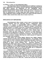
3.7.4.3.
Stoichiometry
and
Properties.
Considerable variation
in
the
composition and properties of reactively sputtered films is possible, depending
on operating conditions. The case of tantalum nitride is worth considering
in
this regard. One
of
the first electronic applications of reactive sputtering
involved deposition of TaN resistors employing dc diode sputtering at voltages
of
3-5
kV,
and pressures of about
30
x
torr.
The dependence
of
the
resistivity
of
"tantalum nitride" films is shown in Fig.
3-23,
where either Ta,
Ta,N, TaN,
or
combinations of these form as a function of N, partial
pressure. Color changes accompany the varied film stoichiometries. For
example, in the case of titanium nitride films, the metallic color
of
Ti gives
way to a light gold, then a rose, and finally a brown color with increasing
nitrogen partial pressure.
3.7.5.
Bias
Sputtering
In
bias sputtering, electric fields near the substrate are modified
in
order to
vary the flux and energy of incident charged species. This is achieved by
applying either a negative dc
or
RF bias to the substrate. With target voltages
of
-
lo00
to
-3OOO
V,
bias voltages of
-50
to
-300
V
are typically used.
Due to charge exchange processes in the anode dark space, very few discharge
ions strike the substrate with full bias voltage. Rather a broad low energy
distribution of ions and neutrals bombard the growing film. The technique has
been utilized in all sputtering configurations (dc, RF, magnetron, and reactive).
130
Physical
Vapor Deposition
(1
7pRcrn)
100
-
b
0
100
200
300
SUBSTRATE BIAS (-VOLTS)
0
Figure
3-24.
thick). (From
Ref.
27).
RF
bias
(1600
A
thick).
(From
Ref.
28).
Resistivity of Ta filmsDvs. substrate bias voltage;
dc
bias
(3000
A
Bias sputtering has been effective
in
altering a broad range of properties
in
deposited films.
As
specific examples we cite (Refs.
4-6).
a.
Resistivity-
A
significant reduction in resistivity has been observed in
metal films such as Ta,
W,
Ni,
Au,
and Cr. The similar variation
in
Ta
film resistivity with dc
or
RF bias shown in Fig.
3-24
suggests that a
common mechanism, independent of sputtering mode, is operative.
b. Hardness and Residual Stress-The hardness of sputtered
Cr
has been
shown to increase (or decrease) with magnitude of negative bias voltage
applied. Residual stress is similarly affected by bias sputtering.
c. Dielectric Properties-Increasing RF bias during RF sputtering of SiO,
films has resulted in decreases in relative dielectric constant, but increases
in resistivity.
d.
Etch
Rate-The wet chemical etch rate of reactively sputtered silicon
nitride films is reduced with increasing negative bias.
e.
Optical Reflectivity-Unbiased films of
W,
Ni, and Fe appear dark gray
or black, whereas bias-sputtered films display metallic luster.
f.
Step Coverage-Substantial improvement in step coverage
of
A1
accompa-
nies application of dc substrate bias.
3.7
Sputtering
Processes
131
g. Film morphology-The columnar microstructure of RF-sputtered Cr is
totally disrupted by ion bombardment and replaced instead by a compacted,
fine-grained structure (Ref.
18).
h. Density-Increased film density has been observed in bias-sputtered Cr
(Ref.
18).
Lower pinhole porosity and corrosion resistance are manifesta-
tions of the enhanced density.
i. Adhesion-Film adhesion is normally improved with ion bombardment
of
substrates during initial stages of film formation.
Although the details are not always clearly understood, there is little doubt
that bias controls the film gas content. For example, chamber gases (e.g., Ar,
O,,
N,,
etc.) sorbed on the growing film surface may be resputtered during
low-energy ion bombardment. In such cases both weakly bound physisorbed
gases (e.g., Ar) or strongly attached chemisorbed species (e.g.,
0
or N on Ta)
apparently have large sputtering yields and low sputter threshold voltages. In
other cases, sorbed gases may have anomalously low sputter yields and will be
incorporated within the growing film. In addition, energetic particle bombard-
ment prior to and during film formation and growth promotes numerous
changes and processes at a microscopic level, including removal of contami-
nants, alteration of surface chemistry, enhancement of nucleation and renucle-
ation (due to generation of nucleation sites via defects, implanted, and recoil-
implanted species), higher surface mobility of adatoms, and elevated film
temperatures with attendant acceleration of atomic reaction and interdiffusion
rates. Film properties are then modified through roughening
of
the surface,
elimination
of
interfacial voids and subsurface porosity, creation
of a finer, more isotropic grain morphology, and elimination
of
columnar
grains-in a way that strongly dramatizes structure-property relationships in
practice.
There are few ways to broadly influence such a wide variety
of thin-film
properties, in
so simple and cheap a manner, than by application of substrate
bias.
3.7.6.
Evaporation versus Sputtering
Now that the details of evaporation and sputtering have been presented, we
compare their characteristics with respect to process variables and resulting
film properties. Distinctions in the stages of vapor species production, trans-
port
through the gas phase, and condensation on substrate surfaces for the two
PVD processes
are
reviewed in tabular
form
in Table
3-7.
132
Physical
Vapor
Deposition
Table
3-7.
Evaporation versus Sputtering
Evaporation Sputtering
A.
Production of Vapor Species
1.
Thermal evaporation mechanism
2.
Low kinetic energy
of
evaporant
atoms (at
1200
K,
E
=
0.1
eV)
3.
Evaporation rate
(Q.
3-2)
(for
M
=
50,
T
=
1500
K,
and
P,
=
=
1.3
x
10'7atoms/cmz-sec.
4.
Directional evaporation according
to cosine law
5.
Fractionation of multicomponent
alloys, decomposition,
and
dissociation of compounds
6.
Availability of high evaporation
source purities
1.
Ion bombardment and collisional
2.
High kinetic energy
of
sputtered
3.
Sputter rate (at
1
mA/cm2 and
momentum transfer
atoms
(E
=
2-30
eV)
s
=
2)
=
3
x
loi6
atoms/cm2-sec
4.
Directional sputtering according to
cosine law at high sputter rates
5.
Generally good maintenance
of
target
stoichiometry, but some
dissociation of compounds.
6.
Sputter targets of all materials
are available; purity varies with
material
B.
The Gas Phase
1.
Evaporant atoms travel in high
or
1.
Sputtered atoms encounter high-
ultrahigh vacuum
(-
10-6-10-10
torr) ambient
(-
100
mtorr)
2.
Thermal velocity of evaporant
io5
cm/sec cm/sec
3.
Mean-free path is larger than
evaporant
-
substrate spacing.
Evaporant atoms undergo no
collisions in vacuum discharge
pressure discharge region
2.
Neutral atom velocity
-
5
x
lo4
3.
Mean-free path is less than target-
substrate spacing. Sputtered atoms
undergo many collisions in the
C.
The Condensed Film
1.
Condensing atoms have relatively
2.
Low gas incorporation
3.
Grain size generally larger than
4.
Few grain orientations (textured
1.
Condensing atoms have high energy
2.
Some gas incorporation
3.
Good
adhesion to substrate
4.
Many grain orientations
low energy
for sputtered
film
films)
3.8.
HYBRiD AND
MODIFIED
PVD
PROCESSES
This chapter concludes with a discussion
of
several
PVD
processes that are
more complex than the conventional ones considered up to this point. They
demonstrate the diversity
of
process hybridization and modification possible in
3.8
Hybrid and Modified
PVD Processes
133
producing films with unusual properties. Ion plating, reactive evaporation, and
ion-beam-assisted deposition will be the processes considered first. In the first
two, the material deposited usually originates from a heated evaporation
source. In
the
third, well-characterized ion beams bombard films deposited by
evaporation or sputtering. The chapter closes with a discussion of ionized
cluster-beam deposition. This process is different from others considered in
this chapter in that film formation occurs through impingement of collective
groups of atoms from the gas phase rather than individual atoms.
3.8.1.
Ion
Plating
Ion plating, developed by Mattox (Ref.
29),
refers to evaporated film deposi-
tion processes in which the substrate
is
exposed to a flux of high-energy ions
capable of causing appreciable sputtering before and during film formation.
A
schematic representation of a diode-type batch, ion-plating system is shown in
Fig. 3-25a. Since it is a hybrid system, provision must be made to sustain the
plasma, cause sputtering, and heat the vapor source. Prior to deposition, the
substrate, negatively biased from
2
to
5
kV,
is subjected to inert-gas ion
bombardment at a pressure in the millitorr range for a time sufficient to
sputter-clean the surface and remove contaminants. Source evaporation is then
begun without interrupting the sputtering, whose rate must obviously be less
than that
of
the deposition rate. Once the interface between film and substrate
has formed, ion bombardment may or may not
be
continued. To circumvent
the relatively high system pressures associated with glow discharges, high-
vacuum ion-plating systems have also been constructed. They rely on directed
ion beams targeted at the substrate. Such systems, which have been limited
thus far to research applications, are discussed in Section
3.8.3.
Perhaps the chief advantage
of
ion plating is the ability to promote extremely
good adhesion between the film and substrate by the ion and particle bombard-
ment mechanisms discussed in Section
3.7.5.
A
second important advantage is
the high “throwing power” when compared with vacuum evaporation. This
results from gas scattering, entrainment, and sputtering of the film, and
enables deposition in recesses and on areas remote from the source-substrate
line of sight. Relatively uniform coating of substrates with complex shapes is
thus achieved. Lastly, the quality of deposited films is frequently enhanced.
The continual bombardment of the growing film by high-energy ions or neutral
atoms and molecules serves to peen and compact it to near bulk densities.
Sputtering of loosely adhering film material, increased surface diffusion, and
reduced shadowing effects serve to suppress undesirable columnar growth.
CATHODE DARK SPACE
SUBSTRATE
SUBSTRATE HOLDER
WORKING
GAS
I
-V
I,
\
MOVEABLE
'
SHUTTER
I
I
ELECTRON BEAM
PRESSURE/
I
v~~l~~
I
'
EVAPORATOR
BARRIER
I
VACUUM
CHAMBER
(a)
SUBSTRATE(S)
ELECTRODE
GAS INJECT1
'1
-0
3
Y
g.
VACUUM
0
PUMPS VACUUM
4
E
<
m
ELECTRON BEAM
EVAPORATOR
CHAMBER
2.
BARR
I
ER
(b)
6
a
Figure
3-25.
Ion-beam-assisted deposition. (From Ref.
3
1).
Hybrid
PVD
process: (a) Ion plating. (From Ref.
29).
(b)
Activated reactive evaporation. (From Ref.
30).
(c)
3.8
-
-
Hybrid and Modified
PVD
Processes
135
(C)
Figure
3-25.
Continued.
A
major use
of
ion plating has been to coat steel and other metals with very
hard films
for
use in tools and wear-resistant applications.
For
this purpose,
metals like Ti,
Zr,
Cr,
and Si are electron-beam-evaporated through an
Ar
plasma in the presence
of
reactive gases such as
N,
,
0,
,
and
CH,
,
which are
simultaneously introduced into the system. This variant
of
the process is
known as reactive ion plating
(RIP),
and coatings
of
nitrides, oxides, and
carbides have been deposited in this manner.
3.8.2.
Reactive Evaporation Processes
In
reactive evaporation the evaporant metal vapor
flux
passes through and
reacts with a gas (at
1-30
X
torr) introduced into the system to produce
compound deposits. The process has a history
of
evolution in which evapora-
tion was first carried out without ionization
of
the reactive gas.
In
the more
recent activated reactive evaporation
(ARE)
processes developed by Bunshah
136
Physical
Vapor
Deposition
and co-workers (Ref.
30),
a plasma discharge is maintained directly within the
reaction zone between the metal source and substrate. Both the metal vapor
and reactive gases, such as
0,,
N,,
CH,, C,H,,
etc., are, therefore, ionized
increasing their reactivity
on
the surface of the growing film or coating,
promoting stoichiometric compound formation. One of the process configura-
tions is illustrated in Fig. 3-25b, where the metal is melted by an electron
beam.
A
thin plasma sheath develops
on
top of the molten pool. Low-energy
secondary electrons from this source are drawn upward into the reaction zone
by a circular wire electrode placed above the melt biased to a positive dc
potential
(20-100
V),
creating a plasma-filled region extending from the
electron-beam gun to near the substrate. The ARE process is endowed with
considerable flexibility, since the substrates can be grounded, allowed to float
electrically, or biased positively or negatively.
In
the latter variant
ARE
is
quite similar
to
RIP. Other modifications of
ARE
include resistance-heated
evaporant sources coupled with a low-voltage cathode (electron) emitter-anode
assembly. Activation by dc and RF excitation has also been employed
to
sustain the plasma, and transverse magnetic fields have been applied
to
effectively extend plasma electron lifetimes.
Before considering the variety of compounds produced by
ARE,
we recall
that thermodynamic and kinetic factors are involved in their formation. The
high negative enthalpies of compound formation of oxides, nitrides, carbides,
and borides indicate
no
thermodynamic obstacles to chemical reaction. The
rate-controlling step in simple reactive evaporation is frequently the speed of
the chemical reaction at the reaction interface. The actual physical location of
the latter may
be
the substrate surface, the gas phase, the surface of the metal
evaporant pool, or a combination of these. Plasma activation generally lowers
the energy barrier for reaction by creating many excited chemical species. By
eliminating the major impediment to reaction,
ARE
processes are thus capable
of deposition rates of a few thousand angstroms per minute.
A
partial list of compounds synthesized by
ARE
methods includes the oxides
aAl,O,,
V,O,, TiO,, indium-tin oxide; the carbides Tic,
ZrC,
NbC, Ta,C,
W2C, VC, HfC; and the nitrides TiN, MoN,
HfN,
and cubic boron nitride.
The extremely hard TiN, Tic,
A120,,
and
HfN
compounds have found
extensive use as coatings for sintered carbide cutting tools, high-speed drills,
and gear cutters.
As
a result, they considerably increase wear resistance and
extend tool life.
In
these applications
ARE
processing competes with the CVD
methods discussed in Chapters
4
and
12.
The fact that no volatile metal-bearing
compound is required as in CVD is an attractive advantage of
ARE.
Most
significantly, these complex compound films are synthesized at relatively low
temperatures; this is a unique feature of plasma-assisted deposition processes.
3.8
Hybrid and Modified
PVD
Processes
137
3.8.3. Ion-Beam-Assisted Deposition Processes (Ref.
31)
We noted in Section
3.7.5
that ion bombardment of biased substrates during
sputtering is a particularly effective way to modify film properties. Process
control in plasmas is somewhat haphazard, however, because the direction,
energy, and flux of the ions incident
on
the growing film cannot be regulated.
Ion-beam-assisted processes were invented to provide independent control
of
the deposition parameters and, particularly, the characteristics of the ions
bombarding the substrate. Two main ion source configurations are employed.
In the dual-ion-beam system, one source provides the inert
or
reactive ion
beam to
sputter
a target in order to yield a flux of atoms for deposition onto
the substrate. Simultaneously, the second ion source, aimed at the substrate,
supplies the inert
or
reactive ion beam that bombards the depositing film.
Separate film-thickness-rate and ion-current monitors, fixed to the substrate
holder, enable the two incident beam fluxes to be independently controlled.
In the second configuration (Fig. 3-25c), an ion source is used in conjunc-
tion with an
evaporation
source. The process, known as ion-assisted deposi-
tion (IAD), combines the benefits of high film deposition rate and ion
bombardment. The energy
flux
and direction of the ion beam can be regulated
independently of the evaporation flux. In both configurations the ion-beam
angle of incidence is not normal to the substrate and can lead to anisotropic
film properties. Substrate rotation is, therefore, recommended if isotropy is
desired.
Broad-beam (Kaufman) ion sources, the heart of ion-beam-assisted deposi-
tion systems, were first used as ion thrusters for space propulsion (Ref.
32).
Their efficiency has been optimized to yield high-ion-beam fluxes for given
power inputs and gas flows. They contain a discharge chamber that is raised to
a potential corresponding to the desired ion energy. Gases fed into the chamber
become ionized in the plasma, and a beam of ions is extracted and accelerated
through matching apertures in a pair of grids. Current densities of several
mA/cm2 are achieved. (Note that
1
mA/cm2 is equivalent to
6.25
x
1015
ions/cm2-sec or several monolayers per second.) The resulting beams have a
low-energy spread (typically
10
eV) and are well collimated, with divergence
angles of only a few degrees. Furthermore, the background pressure is quite
low
(-
Examples of thin-film property modification as a result of
IAD
are given in
Table
3-8.
The reader should appreciate the applicability to all classes of solids
and to a broad spectrum of properties.
For
the most part, ion energies are
lower than those typically involved in sputtering. Bombarding ion fluxes are
generally smaller than depositing atom fluxes. Perhaps the most promising
torr) compared with typical sputtering or etching plasmas.
138
Physical Vapor Deposition
Table
3-8.
Property Modification
by
Ion Bombardment during Film Deposition
Ion Ion/Atom
Film
Ion
property
energy Arrival
material species modified (eV) Rate Ratio
Ge
Nb
Cr
Cr
SiO,
SiO,
AlN
Au
GdCoMo
cu
BN
za2
I
SiO,
,
TiO,
SO2,
TiO,
SO,, TiO,
cu
Ni on Fe
Arf
Ar+
Arf,
Xe+
Ar+
Ar+
Ar+
N:
Ar+
Ar+
cu
+
(B
-
N-H)
+
Ar+,
0:
0:
0:
N+, Ar+
Ar+
Stress,
adhesion
Stress
Stress
Stress
Step
coverage
Step
coverge
Preferred
orientation
Coverage at
50
thickness
Magnetic
anisotropy
Improved
epitaxy
Cubic
structure
Refractive
index,
amor
+
crys
Refractive
index
Optical
transmission
Adhesion
Hardness
65
-
3000
100-400
3,400-11,500
200-800
500
-
1-80
300-500
400
-
1-150
50-400
200-
1000
600
300
30-500
50,000
10,000-20,000
2
x
10-~
to
10-1
3
x
10-2
8
x
to
4
x
10-2
-
7
x
to
2
x
10-2
0.3
-
4.0
0.96
to
1.5
0.1
-
0.1
10-2
-
1.0
2.5
x
lO-’to
10-I
0.12
0.05
to
0.25
-
0.25
From
Ref.
32.
application of ion bombardment is the enhancement of the density and index of
refraction of optical coatings. This subject is treated again in Chapter
11.
3.8.4.
Ionized Cluster Beam (ICB) Deposition (Ref.
33)
The idea of employing energetic ionized clusters of atoms to deposit thin films
is due to
T.
Takagi. In this novel technique, vapor-phase aggregates or
clusters, thought to contain a few hundred to a few thousand atoms, are
3.8
Hybrid and Modified
PVD
Processes
139
SUBSTRATE
I?
!
@
1
@+
:I
\
\
\
I
I
I
I
'\
\
@
\
a++
IONIZED
\
\
I
CLUSTERS
NEUTRAL
ACCELERATING
\
ELECTRODE
\
E
L
ECTRONS
FOR IMPACT
IONIZATION
MATERIAL
I
-NEUTRAL
CLUSTERS
0-10
kV
Figure
3-26.
Schematic diagram of ICB system. (Courtesy
of
W.
L.
Brown,
AT&T
Bell Laboratories. Reprinted
with
permission of the publisher from Ref.
34).
created, ionized, and accelerated toward the substrate as depicted schematically
in Fig.
3-26.
As
a result of impact with the substrate, the cluster breaks apart,
releasing atoms to spread across the surface. Cluster production is, of course,
the critical step and begins with evaporation from a crucible containing a small
aperture or nozzle. The evaporant vapor pressure is much higher
(10-*-10
torr) than in conventional vacuum evaporation. For cluster formation the
nozzle diameter must exceed the mean-free path of vapor atoms in the crucible.
Viscous flow of atoms escaping the nozzle then results in an adiabatic
supersonic expansion and the formation of stable cluster nuclei. Optimum
expansion further requires that the ratio of the vapor pressure in the crucible to
that in the vacuum chamber exceed
lo4
to
10'.
The arrival of ionized clusters with
the
kinetic energy of the acceleration
voltage
(0-10
kV), and neutral clusters with the kinetic energy of the nozzle
ejection velocity, affects film nucleation and growth processes in
the
following
ways:
1.
The
local
temperature at the point
of
impact increases.
2.
Surface diffusion of atoms is enhanced.
140
Physical
Vapor
Deposition
3.
Activated centers for nucleation are created.
4.
Coalescence of nuclei is fostered.
5.
At
high enough energies, the surface is sputter-cleaned, and shallow
implantation of ions may occur.
6.
Chemical reactions between condensing atoms and the substrate
or
gas-phase
atoms are favored.
Moreover, the magnitude of these effects can
be
modified by altering the
extent of electron impact ionization and the accelerating voltage.
Virtually all classes of film materials have been deposited by ICB (and
variant reactive process versions), including pure metals, alloys, intermetallic
compounds, semiconductors, oxides, nitrides, carbides, halides, and organic
compounds. Special attributes of ICB-prepared films
worth
noting are strong
adhesion to the substrate, smooth surfaces, elimination of columnar growth
morphology, low-temperature growth, controllable crystal structures, and,
importantly, very high quality single-crystal growth (epitaxial films). Large Au
film mirrors for CO, lasers, ohmic metal contacts to Si and Gap, electromigra-
tion- (Section
8.4)
resistant A1 films, and epitaxial Si, GaAs, Gap, and InSb
films deposited at low temperatures are some examples indicative of the
excellent properties of ICB films. Among the advantages of ICB deposition are
vacuum cleanliness
(-
lo-’
torr in the chamber) of evaporation and energetic
ion bombardment of the substrate, two normally mutually exclusive features.
In addition, the interaction of slowly moving clusters with the substrate is
confined, limiting the amount of damage to both the growing film and
substrate. Despite the attractive features of ICB, the formation of clusters and
their role in film formation are not well understood. Recent research (Ref.
34),
however, clearly indicates that the total number of atoms agglomerated
in
large
metal clusters is actually very small (only
1
in lo4) and that only a fraction of
large clusters is ionized. The
total
energy brought to the film surface by
ionized clusters is, therefore, quite small. Rather, it appears that individual
atomic ions, which are present in much greater profusion than are ionized
clusters, are the dominant vehicle for transporting energy and momentum to
the growing film. In this respect, ICB deposition belongs to the class of
processes deriving benefits from the ion-beam-assisted film growth mecha-
nisms previously discussed.
EXERCISES
1.
Employing Figs.
3-1
and
3-2,
calculate values for
the
molar heat of
vaporization
of
Si and Ga.
Exercises
141
2.
Design a laboratory experiment to determine a working value of the heat
of vaporization of a metal employing common thin-film deposition and
characterization equipment.
3.
Suppose Fe satisfactorily evaporates from a surface source,
1
cm2 in
area, which is maintained at
1550
"C.
Higher desired evaporation rates
are achieved by raising the temperature
100
"C. But doing this will bum
out the source. Instead, the melt area is increased without raising its
temperature. By what factor should the source area be enlarged?
4.
A molecular-beam epitaxy system contains separate A1 and As effusion
evaporation sources of
4
cm2 area, located
10
cm from a
(100)
GaAs
substrate. The A1 source is heated to
10oO
"C,
and the As source is
heated to
300
"C.
What is the growth rate of the AlAs film in Alsec?
[Note: AlAs basically has the same crystal structure and lattice parameter
(5.661
A)
as
GaAs.]
5. How far from the substrate, in illustrative problem on p.
90,
would a
single surface source have to
be
located to maintain the same deposited
film thickness tolerance?
6. An A1 film was deposited at a rate of
1
pmlmin in vacuum at
25
'C,
and
What was
it was estimated that the oxygen content of the film was
the partial pressure of oxygen in the system?
7.
Alloy films of Ti-W, used as diffusion barriers
in
integrated circuits, are
usually sputtered. The Ti-W, phase diagram resembles that
of
Ge-Si
(Fig.
1
-
13)
at elevated temperatures.
a. Comment on the ease
or
feasibility
of
evaporating a
15
wt% Ti-W
b.
During sputtering with 0.5-keV Ar, what composition will the target
alloy.
surface assume in the steady state?
8.
In order to deposit films of the alloy YBa,Cu,
,
the metals Y, Ba, and
Cu
are evaporated from three point sources. The latter are situated at the
comers
of
an equilateral triangle whose side
is
20
cm. Directly above the
centroid of the source array, and parallel to it, lies a small substrate; the
deposition system geometry is thus a tetrahedron, each side being
20
cm
long.
a.
If the
Y
source is heated to
1740
K
to produce a vapor pressure of
torr, to what temperature must the
Cu
source be heated to
maintain film stoichiometry?
142
Physical
Vapor
Deposition
b. Rather than a point source, a surface source is used to evaporate Cu.
How must the Cu source temperature
be
changed to ensure deposit
stoichiometry?
c. If
the
source configuration in part (a) is employed, what
minimum
0,
partial pressure is required to deposit stoichiometric YBa,Cu,O,
superconducting films by a reactive evaporation process? The atomic
weights are Y
=
89,
Cu
=
63.5,
Ba
=
137,
and
0
=
16.
9.
One way to deposit a thin metal film of known thickness is to heat an
evaporation source to dryness (i.e., until no metal remains in the crucible).
Suppose it is desired to deposit
5000
of Au on the internal spherical
surface of a hemispherical shell measuring
30
cm in diameter.
a. Suggest two different evaporation source configurations (source type
b. What weight of Au would be required for each configuration, assum-
10.
Suppose the processes of electron impact ionization and secondary emis-
sion
of
electrons by ions control the current
J
in a sputtering system
according to the Townsend equation (Ref.
19)
and placement) that would yield uniform coatings.
ing evaporation to dryness?
J,exp
ad
1
-
y[exp(ad)
-
11
'
J=
where
J,
=
primary electron current density from external source
CY
=
number of ions per unit length produced by electrons
y
=
number of secondary electrons emitted
per
incident ion
d
=
interelectrode spacing.
a. If the film deposition rate during sputtering is proportional to the
product of
J
and
S,
calculate the proportionality constant for Cu
in
this system
if
the deposition rate is
200
i/min for 0.5-keV Ar ions.
Assume
CY
=
0.1
ion/cm,
y
=
0.08
electron/ion,
d
=
10
cm, and
J,,
=
100
mA/cm2.
b.
What deposition rate can be expected for 1-keV
Ar
if
a
=
0.15
ion/cm and
y
=
0.1
electron/ion.
11.
In a dc planar magnetron system operating at
lo00
V,
the anode-cathode
spacing
is
10
cm. What magnetic field should be applied to trap electrons
within
1
cm
of
the target?
12.
At what sputter deposition rate of In on a Si substrate will the film melt
within
1
min? The melting point
of
In is
155
"C.
Exercises
143
13.
a. During magnetron sputtering of Au at
1
keV, suppose there are two
collisions with Ar atoms prior to deposition. What is the energy of the
depositing Au atoms? (Assume Ar is stationary in a collision.)
b. The probability that gas-phase atoms will travel a distance
x
without
collision is exp
-
x/X,
where
X
is the mean-free path between
collisions. Assume
X
for Au in Ar is
5
cm at a pressure of
1
mtorr. If
the target-anode spacing is 12 cm, at what operating pressure will
99%
of the sputtered Au atoms undergo gas-phase collisions prior to
deposition?
14.
For a new application it is desired to continuously coat a 1-m-wide steel
strip with a 2-pm-thick coating of Al. The
x-y
dimensions of the steel are
such that an array of electron-beam gun evaporators lies along the
y
direction and maintains a uniform coating thickness across the strip width.
How fast should the steel be fed in the
x
direction past the surface
sources, which can evaporate
20
g of A1 per second? Assume that
Eq.
3-18 holds for the coating thickness along the
x
direction, that the
source-strip distance is
30
cm, and that the steel sheet is essentially a
horizontal substrate
40 cm long on either side of the source before it
is
coiled.
1
5.
Select the appropriate film deposition process (evaporation, sputtering,
etc., sources, targets, etc.) for the following applications:
a. Coating a large telescope mirror with
Rh
b. Web coating
of
potato chip bags with A1 films
c. Deposition of AI-Cu-Si thin-film interconnections for integrated cir-
d. Deposition of Ti0,-SO, multilayers on artificial gems to enhance
cuits
color and reflectivity
1
6.
Theory indicates that the kinetic energy
(E)
and angular spread of neutral
atoms sputtered from a surface are given by the distribution function
E
(E
+
U)’
F(E,
e)
=
cs cos
e,
where
U
=
binding energy of surface atoms
C
=
constant
0
=
angle between sputtered atoms and the surface normal.
a.
Sketch the dependence of
f(
E,
e)
vs.
E
for two values of
U.
b. Show that the maximum in the energy distribution occurs at
E
=
U/2.
144
Physical
Vapor
Deposition
17.
a.
To
better visualize the nucleation of clusters in the ICB process,
schematically indicate the free energy of cluster formation vs. cluster
size as a function
of
vapor supersaturation (see Section 1.7).
b. What vapor supersaturation is required to create a 1000-atom cluster
of Au if the surface tension is 1000 ergs/cm*?
c.
If
such a cluster is ionized and accelerated to an energy
of
10 keV,
how much energy is imparted to the substrate by each cluster atom?
REFERENCES
1. W.
R.
Grove,
Phil. Trans. Roy. Soc., London
A
142,
87 (1852).
2.
M. Faraday,
Phil. Trans.
147,
145 (1857).
3.*
R.
Glang, in
Handbook
of
Thin Film Technology,
eds.
L.
I. Maissel
and
R.
Glang, McGraw-Hill, New York (1970).
4.*
J.
L. Vossen and
J. J.
Cuomo, in
Thin Film Processes,
eds.
J.
L.
Vossen and W. Kern, Academic Press, New York (1978).
5.*
W.
D. Westwood, in
Microelectronic Materials and Processes,
ed.
R.
A. Levy, Kluwer Academic, Dordrecht (1989).
6.*
B.
N. Chapman,
Glow Discharge Processes,
Wiley, New York (1980).
7. C. H. P. Lupis,
Chemical Thermodynamics
of
Materials,
North-Hol-
land, Amsterdam (1983).
8.
R.
E. Honig,
RCA Rev.
23,
567 (1962).
9.* H. K. Pulker,
Coatings on Glass,
Elsevier, New York, (1984).
10.
11.
12.
13.
14.
15.
16.
Examples taken from
Physical Vapor Deposition,
Airco-Temescal
(1976).
L. Holland,
Vacuum Deposition
of
Thin Films,
Wiley, New York
(1956).
C. H. Ting and A.
R.
Neureuther,
Solid State Technol.
25(2),
115
(1982).
H. L. Caswell, in
Physics
of
Thin Films,
Vol. 1, ed. G. Hass,
Academic Press, New York (1963).
L. D. Hartsough and D.
R.
Denison,
Solid State Technology
22(12),
66 (1979).
Handbook- The Optical Industry and Systems Directory,
H-1 1
(1979).
E.
B.
Grapper,
J.
Vac. Sci. Technol.
5A(4),
2718 (1987);
8,
333
(1971).
*Recommended texts
or
reviews.
References
145
17. P. Archibald and E. Parent,
Solid State Technol.
19(7),
32 (1976).
18.
D.
M. Mattox,
J.
Vac. Sci. Technol.
A7(3),
1105 (1989).
19.*
A. B. Glaser and G.
E.
Subak-Sharpe,
Integrated Circuit Engineering,
Addison-Wesley
,
Reading, MA
(
1979).
20. P. Sigmund, Phys.
Rev.
184,
383 (1969).
21.
L.
T. Lamont,
Solid Stale Technol.
22(9),
107 (1979).
22. J. A. Thornton,
Thin Solid Films
54,
23 (1978).
23. J. A. Thornton, in
Thin Film Processes,
eds. J.
L.
Vossen and W.
Kern, Academic Press, New York (1978).
24. H. R. Koenig and
L.
I.
Maissel,
IBM
J.
Res. Dev.
14,
168 (1970).
25.* W.
D.
Westwood, in
Physics
of
Thin Films,
Vol. 14, eds. M. H.
Francombe and J.
L.
Vossen, Academic Press, New York (1989).
26.*
L.
I.
Maissel and M. H. Francombe,
An
Introduction to Thin Films,
Gordon and Breach, New York, (1973).
27.
L.
I.
Maissel and P. M. Schaible,
J.
Appl.
Plzys.
36,
237 (1965).
28. J.
L.
Vossen and J. J. O’Neill,
RCA
Rev.
29,
566 (1968).
29. D. M. Mattox,
J.
Vac. Sci. Technol.
10,
47 (1973).
30.*
R.
F. Bunshah and
C.
Deshpandey, in
Physics of Thin Films,
Vol. 13,
eds.
M.
H.
Francombe and J.
L.
Vossen, Academic Press, New York
(1987).
J.
M.
E.
Harper and
J.
J.
Cuomo,
J.
Vuc.
Sci.
Technol.
21(3),
737 (1982).
J. M. E. Harper, J. J. Cuomo, R. J. Gambino, and
H.
R. Kaufman, in
Ion Beam Modification of Surfaces,
eds.
0.
Auciello and R. Kelly,
Elsevier, Amsterdam (1984).
33.* T. Takagi, in
Physics of Thin Films,
Vol. 13, eds. M.
H.
Francombe
and J.
L.
Vossen, Academic Press, New York (1987).
34. W.
L.
Brown, M. F. Jarrold, R.
L.
McEachern,
M.
Ssnowski, G.
Takaoka, H. Usui and
I.
Yamada,
Nuclear Instruments and Methods
in Physics Research,
to
be
published (1991).
31.
32.
Chapter
4
w
Chemical Vapor Deposition
4.1.
INTRODUCTION
Chemical vapor deposition
(CVD)
is the process of chemically reacting a
volatile compound of a material to be deposited, with other gases, to produce a
nonvolatile solid that deposits atomistically on a suitably placed substrate.
High-temperature
CVD
processes for producing thin films and coatings have
found increasing applications in such diverse technologies as the fabrication
of
solid-state electronic devices, the manufacture of ball bearings and cutting
tools, and the production
of
rocket engine and nuclear reactor components. In
particular, the need for high-quality epitaxial semiconductor films for both
Si
bipolar and
MOS
transistors, coupled with the necessity to deposit various
insulating and passivating films at low temperatures, has served as a powerful
impetus to spur development and implementation of
CVD
processing methods.
A
schematic view
of
the
MOS
field effect transistor structure
in
Fig.
4-1
indicates the extent to which the technology is employed. Above the plane of
the base P-Si wafer, all
of
the films with the exception
of
the gate oxide and
A1 metallization are deposited by some variant
of
CVD
processing. The films
include polysilicon, dielectric SO,, and SIN.
Among the reasons for the growing adoption of
CVD
methods
is
the ability
to produce a large variety of films and coatings of metals, semiconductors, and
147
148
Chemical
Vapor
Deposition
DIELECTRIC
SIN
WAFER
Figure
4-1.
Schematic view
of
MOS
field effect transistor cross section
compounds in either a crystalline
or
vitreous form, possessing high purity and
desirable properties. Furthermore, the capability of controllably creating films
of
widely varying stoichiometry makes CVD unique among deposition tech-
niques. Other advantages include relatively low cost
of
the equipment and
operating expenses, suitability for both batch and semicontinuous operation,
and compatibility with other processing steps. Hence, many variants
of
CVD
processing have been researched and developed in recent years, including
low-pressure (LPCVD), plasma-enhanced (PECVD), and laser-enhanced
(LECVD) chemical vapor deposition. Hybrid processes combining features
of
both physical and chemical vapor deposition have also emerged.
In this chapter, a number of topics related to the basic chemistry, physics,
engineering, and materials science involved in CVD are explored. Practical
concerns
of
chemical vapor transport, deposition processes, and equipment
involved are discussed. The chapter is divided into the following sections:
4.2.
Reaction Types
4.3.
Thermodynamics
of
CVD
4.4.
Gas Transport
4.5.
Growth Kinetics
4.6.
CVD Processes and Systems
Recommended review articles and books dealing with these aspects
of
CVD
can be found
in
Refs.
1
-7.
To gain an appreciation of the scope
of
the subject, we first briefly
categorize the various types
of
chemical reactions that have been employed to
deposit films and coatings (Refs.
1-3).
Corresponding examples are given for
each by indicating the essential overall chemical equation and approximate
reaction temperature.
4.2.
Reaction
Types
149
4.2.
REACTION
TYPES
4.2.1.
Pyrolysis
Pyrolysis involves the thermal decomposition of such gaseous species as
hydrides, carbonyls, and organometallic compounds on hot substrates. Com-
mercially important examples include the high-temperature pyrolysis of silane
to produce polycrystalline
or
amorphous silicon films, and the low-temperature
decomposition of nickel carbonyl to deposit nickel films.
SiH,(,,
-+
Si,,,
+
2H,(,,
(650
"C), (4-1)
Ni(CO)qyg,
+
Ni,,,
+
4CO(,,
(180
"C).
(4-2)
Interestingly, the latter reaction is the basis of the Mond process, which has
been employed for over a century in the metallurgical refining of Ni.
4.2.2.
Reduction
These reactions commonly employ hydrogen gas as the reducing agent to effect
the reduction of such gaseous species as halides, carbonyl halides, oxyhalides,
or
other oxygen-containing compounds. An important example is the reduction
of SiCl, on single-crystal Si wafers to produce epitaxial Si films according to
the reaction
SiCl,(,)
+
2H2(,,
+
Si,,,
+
4HC1(,, (1200 "C). (4-3)
Refractory metal films such as
W
and Mo have been deposited by reducing the
corresponding hexafluorides, e.g.,
wF6(g)
+
3H2(g)
-+
w(s)
+
6HF(g)
(300
"C), (4-4)
M°F6(g)
+
3H2(g)
-b
Mo(5)
+
6HF(g)
(300 "C). (4-5)
Tungsten films deposited at low temperatures have been actively investigated
as a potential replacement for aluminum contacts and interconnections
in
integrated circuits. Interestingly,
WF,
gas reacts directly with exposed silicon
surfaces, depositing thin
W
films while releasing the volatile
SiF,
by-product.
In this way silicon contact holes can
be
selectively filled with tungsten while
leaving neighboring insulator surfaces uncoated.
150
Chemical
Vapor
Deposition
4.2.3.
Oxidation
Two examples of important oxidation reactions are
SiH4,,,
+
o,,,,
-+
sio2,,,
+
2H2(,, (450 "C), (4-6)
4PH,(,,
+
50,,,,
+
2P,O,,,,
+
6H,(,,
(450
"C).
(4-7)
The deposition of SiO, by Eq. 4-6 is often carried out at a stage in the
processing of integrated circuits where higher substrate temperatures cannot be
tolerated. Frequently, about
7
%
phosphorous is simultaneously incorporated in
the Si02 film by the reaction of Eq. 4-7 in order to produce a glass film that
flows readily to produce a planar insulating surface, i.e., "planarization."
In another process of technological significance, SiO, is
also
produced by
the oxidation reaction
(1500 "C). (4-8)
The eventual application here is the production of optical fiber for communica-
tions purposes. Rather than a thin film, the
SiO,
forms a cotton-candy-like
deposit consisting of soot particles less than
loo0
in size. These are then
consolidated by elevated temperature sintering to produce a fully dense silica
rod for subsequent drawing into fiber. Whether silica film deposition
or
soot
formation occurs is governed by process variables favorable to heterogeneous
or
homogeneous nucleation, respectively. Homogeneous soot formation is
essentially the result of a high SiCl, concentration in the gas phase.
SiCl,,,,
+
2H,,,,
+
O,,,,
-+
SiO,(,,
+
4HC1,,,
4.2.4.
Compound Formation
A
variety
of
carbide, nitride, boride, etc., films and coatings can be readily
produced by CVD techniques. What is required is that the compound elements
exist
in
a volatile form and be sufficiently reactive in the gas phase. Examples
of commercially important reactions include
SiCl,(,,
+
CH,(,,
-P
Sic,,,
+
4HC1,,,
(4-9)
TiCl,,,,
+
CH,,,,
-+
TIC,,,
+
4HC1,,,
(loo0
"C), (4-10)
(1400
"C)
,
BF,,,,
+
NH,,,, BN,,,
+
3%)
(1
100
"C)
(4-1
1)
for the deposition of hard, wear-resistant surface coatings. Films and coatings
of
compounds can generally be produced through a variety of precursor gases
and reactions. For example, in the much studied Sic system, layers were first
4.2.
Reaction
Types
151
produced in
1909
through reaction of SiC1,
+
C,H, (Ref.
8).
Subsequent
reactant combinations over the years have included SiCI,
+
C,H,
,
SiBr,
+
C,H,, SiC1,
+
C6H,,
,
SiHCl,
+
CCI,, and SiC1,
+
C,H,CH,, to name a
few, as well as volatile organic compounds containing both silicon and carbon
in the same molecule (e.g., CH,SiCl,, CH,SiH,, (CH3)2SiC12, etc.). Al-
though the deposit is nominally Sic in
all
cases, resultant properties generally
differ because of structural, compositional, and processing differences.
Impermeable insulating and passivating films of Si,N, that are used in
integrated circuits can
be
deposited at
750
"C by the reaction
3SiC1,H2(,,
+
4NH,(,,
-,
Si3N4(s,
+
6H,,,,
+
6HC1(,,
.
(4-12)
The necessity to deposit silicon nitride films at lower temperatures has led to
alternative processing involving the use
of
plasmas. Films can be deposited
below
300
"C with SiH, and NH, reactants, but considerable amounts of
hydrogen are incorporated into the deposits.
4.2.5. Disproportionation
Disproportionation reactions are possible when a nonvolatile metal can form
volatile compounds having different degrees of stability, depending on the
temperature. This manifests itself in compounds, typically halides, where the
metal exists in two valence states (e.g.,
GeI, and GeI,) such that the
lower-valent state is more stable at higher temperatures. As a result, the metal
can be transported into the vapor phase by reacting it with its volatile,
higher-valent halide to produce the more stable lower-valent halide. The latter
disproportionates at lower temperatures to produce a deposit of metal while
regenerating the higher-valent halide. This complex sequence can be simply
described by the reversible reaction
and realized in systems where provision is made
for
mass transport between
hot and cold ends. Elements that have lent themselves
to
this type of transport
reaction include aluminum, boron, gallium, indium, silicon, titanium, zirco-
nium, beryllium, and chromium. Single-crystal films
of
Si
and Ge were grown
by disproportionation reactions
in
the early days of
CVD
experimentation on
semiconductors employing reactors such as that shown in Fig.
4-2.
The
enormous progress made in this area is revealed here.
152
Chemical
Vapor
Deposition
THERMOCOUPLE
SUBSTRATE
SI
LEON
ASBESTOS WRAP
HEATER WlNDlN
REACTION TUBE
SUBSTRATE REG
I
ON
Si1
+
Si
c
2Si12
Si
+
21,
-
Si14
Sild
+
Si
-
2Si12
SOURCE REGION
TEMPERATURE
(OC)
Figure
4-2.
Experimental reactor
for
epitaxial
growth
of
Si
films.
(E.
S.
Wajda,
B.
W. Kippenhan, W.
H.
White,
ZBM
J.
Res.
Dev.
7,
288,
0
1960
by
International
Business Machines Corporation, reprinted with permission).
4.2.6.
Reversible Transfer
Chemical transfer or transport processes are characterized by a reversal in the
reaction equilibrium at source and deposition regions maintained at different
temperatures within a single reactor. An important example
is
the deposition of
single-crystal (epitaxial) GaAs films by the chloride process according to the
reaction
750
'C
I
As4(,)
+
Asz(,)
+
6GaC1(,,
+
3Hz(,)850+&jGaA~(S)
+
6HC1,,, .
(4-14)
Here AsC1, gas from a bubbler transports Ga toward the substrates in the form
of
GaCl vapor. Subsequent reaction with As, causes deposition
of
GaAs.