The Materials Science of Thin Films 2011 Part 14 doc
Bạn đang xem bản rút gọn của tài liệu. Xem và tải ngay bản đầy đủ của tài liệu tại đây (1.95 MB, 50 trang )
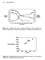
628
Modification
of
Surfaces and Films
24.
J.
K.
Hirvonen
and
C.
R.
Clayton,
in
Surface Modifcation and
Alloying,
eds.
J.
M.
Poate, G. Foti, and
D.
Jacobson, Plenum Press,
New York
(1983).
25.*
G.
K.
Wehner,
J.
Vac. Sci. Tech.
A3,
1821 (1985).
26.
P.
Auciello and
R.
Kelly,
Ion
Bombardment Modification
of
Surfaces
-Fundamentals and Applications,
Elsevier, Amsterdam
(1984).
27.
J.
L.
Whitton,
G.
Carter,
and
M.
J.
Nobes,
Radiation Effects
32,
129
(1977).
28.
G.
K.
Celler,
Solid State Technology
30(3),
69 (1987).
29.
A.
E.
White
and
K.
T.
Short,
Science
241(8),
930 (1988).
hapter
74
3Esk-
Emerging Thin-Film
Materials and Applications
In this final chapter an attempt is made to present a perspective of some
emerging thin-film materials and applications that promise to have a significant
impact on future technology. For this reason the discussion will be limited to
the following topics:
14.1.
Film-Patterning Techniques
14.2.
Diamond Films
14.3.
High
T,
Superconductor Films
14.4.
Films for Magnetic Recording
14.5.
Optical Recording
14.6.
Integrated Optics
14.7.
Superlattices
14.8.
Band-Gap Engineering and Quantum Devices
This potpourri
of
subjects encompasses covalent, metallic, and semiconduc-
tor film materials deposited by an assortment of PVD and
CVD
methods.
Represented are mechanical, electrical, magnetic, and optical properties, whose
optimization hinges on both processing and the ability to characterize struc-
ture-property relationships. Thus the spirit
of
materials science
of
thin
films-the theme and title
of
this book-is preserved in microcosm within this
chapter. For completeness however, it
is
necessary to
start
with Section
14.1,
629
630
Emerging Thin-Film Materials and Applications
which is devoted to the topic
of
thin-film patterning techniques. This subject is
crucial to the realization
of
the intricate lateral geometries and dimensions that
films must assume in varied applications, particularly some
of
those in this
chapter.
14.1.
FILM-PATTERNING TECHNIQUES
14.1
.l.
Lithography
Until now
the
only film dimension considered has been the thickness, which is
controlled by the
growth
or
deposition process. However, irrespective
of
eventual application, thin films must also
be
geometrically defined laterally
or
patterned in the film plane. The complexity
of
patterning processes depends on
the nature
of
the film, the feature dimensions, and the
spatial
tolerance of the
feature dimensions.
For
example, consider an evaporated metai film that must
$.
JJJJ$+J
ULTRAVIOLET RADIATION
MASK
"
I
POSITIVE RESIST
'
NEGATIVE RESIST
Figure
14-1.
Schematic
of
the
lithographic process for
pattern
transfer from mask
to
film.
Both
positive and negative resist behavior
is
illustrated.
14.1.
Filmpatterning Techniques
631
possess features 1 mm in size with a tolerance of
kO.05
mm. The desired
pattern could possibly
be
machined into a thin sheet stencil
or
mechanical
mask. Direct contact between this mask template and substrate ensures genera-
tion of the desired pattern in uncovered regions exposed to the evaporation
flux.
This method is obviously too crude to permit the patterning of features
100
to
loo0
times smaller in size that are employed in integrated circuits. Such
demanding applications require lithographic techniques.
The lithographic process shown schematically in Fig. 14-1 consists of four
steps.
74.7.7.7.
Generation
of
the
Mask.
The mask is essentially equivalent to
the negative in photography. It possesses the desired film geometry patterned
in Cr or FeO thin
films
predeposited
on
a glass
or
quartz plate. Masks for
integrated circuit use are generated employing computer-driven electron
beams
to precisely define regions that are either opaque
or
transparent to light.
Other processing steps to initially produce the patterned mask
film
parallel
those used
in
subsequent pattern transfer to the involved
film.
74.7.7.2.
Printing.
Printing of this negative mask requires the physical
transfer
of
the pattern to the film surface in question. This
is
accomplished by
first spin-coating the film-substrate with a thin photoresist layer
(<
1
pm
thick).
As
the name implies, photoresists are both sensitive to photons and
resistant to chemical attack after exposure and development. Photoresists are
complex photosensitive organic mixtures, usually consisting of a resin, photo-
sensitizer, and solvent. During exposure, light (usually
UV)
passes through the
mask and is imaged on the resist surface by appropriate exposure tools or
printers. Either full-scale or reduced latent images can be produced in the
photoresist layer. There are two types of photoresists and their behaviors are
distinguished in Fig. 14-1. The positive photoresist faithfully reproduces the
(opaque) mask film pattern; in
this
case light exposure causes scission
of
polymerized chains rendering the resist soluble in the developer. Alternatively,
negative resists reproduce
the
transparent portion of the mask pattern because
photon-induced polymerization leaves a chemically inert resist layer behind.
For yet greater feature resolution X-ray
and
electron-beam lithography tech-
niques are practiced.
14.1.1.3.
Etching.
After resist exposure and development, the underlying
film
is
etched. Wet etching in appropriate solutions dissolves away the exposed
632
Emerging Thin-Film Materials and Applications
film, leaving intact the film protected by resist. Equal rates
of
lateral and
vertical material removal (isotropic etching) however,
lead
to
loss of resolution
due to undercutting
of
film features. This presents a problem in VLSI
processing where
1
pm (or
so)
features must be defined. For this reason dry
etching
is
practiced. Material is removed in this
case
through exposure to
reactive plasmas that interact with film atoms to produce volatile by-products
that are pumped away. For example, typical dry etchants for Si, SiO, and Al
are
SF,
+
Cl,,
CF,
+
H,,
and BCl,
+
C1,
gas
mixtures, respectively (Ref.
1).
Alternatively, inert-gas plasmas are also employed
to
erode
the film surface
in a process that resembles the inverse
of
sputtering deposition. In both cases,
positive ion bombardment normal to the surface leads to greater vertical than
horizontal etching, i.e., anisotropic etching. Steep sidewall topography and high
aspect ratio features such
as
shown in Fig.
14-2
are the result
of
anisotropic
material removal.
An important issue in dry etching is the etchant selectivity or ability to
preferentially react with one film species relative to others that are present.
Simply changing the plasma gas composition can significantly alter etching
selectivity. For example, the SiO, etch rate exceeds that
of
poly-Si by only
25%
in a pure CF, plasma. In an equimolar mixture
of
H,
+
CF,
,
however,
Figure 14-2.
SEM
micrograph
of
reactive plasma-etched pattern in photoresist re-
vealing development
of
submicron features. (Courtesy
of
L.
F.
Thompson,
AT&T
Bell
Laboratories).
14.1.
Film-Patterning Techniques
633
the etch rate of poly-Si drops almost
to
zero; the selectivity or ratio of etch rate
of SiO, relative to poly-Si exceeds
45
(Ref. 1).
74.7.1.4.
Resist
Removal.
The final step requires removal of the resist.
Special resist stripper solutions or plasmas (e.g.,
0,
rich)
are
utilized for this
purpose. What remains is a high fidelity thin-film copy
of
the mask geometry.
Only the briefest summary of the basic steps comprising the very important
technology
of
lithography has been presented. For more detailed accounts
of
mask production (Ref.
2),
photoresists (Ref.
3),
printing (Ref.
4),
and etching
(Ref. 1) the reader is referred to the indicated references.
14.1.2.
Silicon Micromachining
Silicon micromachining can
be
defined as a high-precision shaping technique
that uses photolithographic and etching methods to
form
miniature three-di-
mensional shapes in Si (and SO,) such
as
holes, wells, pyramids, grooves,
hemispheres, needles, etc. In the same way that Si has revolutionized electron-
ics, this versatile material has altered conventional perceptions of miniature
mechanical components, devices and systems. Though small, micromachined
features are generally large compared to
VLSI
dimensions. Examples include
the microcantilever thin film beams discussed on p.
412,
tiny gears, valves,
springs and tweezers, X-ray Fresnel lenses, pressure and strain transducers,
ink jet nozzle arrays, electrochemical sensors, multisocket electrical connec-
tors, and force and acceleration transducers (Refs.
5,
6).
Among the recent
developments are the fabrication
of
a triode vacuum microelectronic device
(Ref.
7)
and an optical microassembly. The former shown in Fig. 14-3a
is
impervious to radiation damage, insensitive to heat with the potential for very
VACUUM SPACE
METAL ANODE
INSULATING LAYER
METAL GATE
OR
GRID
*-DIELECTRIC (SUCH
AS
Si021
METAL EMITTER
+-SILICON
SUBSTRATE
Figure
14-3a.
Schematic
structure
of
Si
triode vacuum microelectronic device.
(From
Ref.
7).
634
Emerging Thin-Film Materials and Applications
Figure
14-3b.
SEM
micrograph
of
optical microassembly. (Courtesy
of
K.
L.
Tai,
AT&T Bell Laboratories).
high frequency operation. The latter shown in Fig. 14-3b has been employed to
provide low-loss coupling between optical fibers and optoelectronic devices in
optical communications systems. Here the laser (or detector) rests beneath the
apex of the etched pyramid in which the optical fiber is precisely positioned.
This
microassembly package provides for low-loss electrical interconnection
between optoelectronic and other electronic devices on
a
common Si substrate.
Precise knowledge
of
etch rate anisotropies and selectivities for Si and SiO,
is required for designing successful micromachining etching treatments. In a
recent study (Ref.
8),
utilizing KOH/H,O etchants, the following etch rates
(R)
were measured
as
a function of temperature:
0.61 eV
kT
RSi(100)
=
6.19
x
108exp
-
-
(Ccm/min)
9
(14-1)
0.77 eV
kT
Rsi(lll)
=
3.19
x
l0’exp
-
-
(Ccm/min)
9
(14-2)
1.07 eV
kT
RSiO2
=
5.49
x
10”exp
-
-
(~cm/min),
(14-3)
14.2.
Diamond
Films
635
d
n100
=
T
(X
+
A@
sin
54.7"
Rlll
=
t
Figure
14-4. Etching geometry
of
Si-SiO,
structure.
The ratio Rsi(lOO)/Rsi(lll) defines the etch rate anisotropy
(
Aloo,,l,)
and
the ratio
Rsi(
100)/Rsio2 represents the selectivity.
As
an example in the use
of
these etch rates consider a (100) Si wafer
containing a 2 pm thermally grown SiO, film
so
patterned to open windows to
the Si surface (Fig. 14-4). After etching at 100
"C
for 15 min, how much does
the SiO, etch mask overhang the slanted Si wall? During etching, both the
(100) and (11 1) planes recede along their direction normals. The angle between
the
[
1001 and
[l
1 13 directions
is
54.7". Therefore geometric considerations
indicate that the net overhang length
x
at any time
t
is given by
x
=
(~~~(lll)/sin54.7
-
~,~~,)t,
04-41
where the isotropic etching
of
SiO, is accounted for. Direct substitution
of
RSi(lll)
=
0.126 pm/min, Rsi020.0191 pm/min,
t
=
15
min, and sin54.7
=
0.816, yields
x
=
2.03
pm. Depending on the width of the SiO, mask
window, V-shaped pits or flat-bottomed troughs can be etched into
Si.
14.2.
DIAMOND
FILMS
14.2.1.
Introduction
Derived from the Greek
01Bap01~
(adamas),
which means unconquerable,
diamond
is
indeed
an
invincible material. In addition to being the most costly
636
Emerging Thin-Film Materials and Applications
on a unit weight basis, and capable of unmatched beauty when polished,
diamond has a number of other remarkable properties. It is the hardest
substance known
(H,
>
8OOO
kg/mm2), and has a higher modulus
of
elasticity
(E
=
1050
GPa) than any other material. When free of impurities, it has one
of the highest resistivities
(p
>
1OI6
Q-cm). It also combines a very high
thermal conductivity
(
K
=
1100
W/m-K) that exceeds that of
Cu
and Ag, with
a low thermal expansion coefficient
(a
=
1.2
x
lop6
K-'
)
to yield high
resistance to thermal shock. Lastly, diamond is very resistant to chemical
attack. These facts, the first three, in particular, have spurred one of the most
exciting and competitive quests in the history of materials science-the synthe-
sis of diamond. Success was achieved in
1954
with the General Electric
Corp.
process for producing bulk diamond utilizing extremely high pressures and
temperatures. Interestingly, however, attempts to produce diamond from low-
pressure vapors date back at least to
1911
(Ref.
9).
P. D. Bridgeman, in a
1955
Scientific
American
article, speculated that diamond powders and films
should be attainable by vapor deposition at low pressures (Ref.
10).
By the
mid-
1970s
the Russian investigators Derjaguin and Fedeseev had apparently
grown epitaxial diamond films and whiskers during the pyrolysis of various
hydrocarbon-hydrogen gas mixtures (Ref.
11).
After a decade of relative
quiet, an explosive worldwide interest in the synthesis of diamond films and in
their properties erupted, which persists unabated to the present day.
Isolated
C atoms have distinct
2s
and
2p
atomic orbitals. When these atoms
condense
to
form diamond, electronic admixtures occur, resulting in four equal
hybridized sp3 molecular orbitals. Each
C atom is covalently attached to four
other atoms in tetragonal bonds
1.54
A long creating the well-known diamond
cubic structure (Fig.
1-2c).
Graphite, on the other hand, has a layered
structure. The
C atoms are arranged hexagonally with strong trigonal bonds
(sp2) and have an interatomic spacing
of
1.42
in the basal plane. A fourth
electron in the outer shell forms weak van der Waals bonds between planes that
account for such properties as good electrical conductivity, lubricity, lower
density, a grayish-black color and softness.
In addition,
C
exists in a variety of metastable and amorphous forms that
have been characterized as degenerate or imperfect graphitic structures. In
these, the layer planes are disoriented with respect to
the
common
axis
and
overlap each other irregularly. Beyond the short-range graphitic structure, the
matrix consists of amorphous
C. A complex picture now emerges of the
manifestations of
C
ranging from amorphous to crystalline forms in a contin-
uum of structural admixtures. Similarly, the proportions
of
sp2-sp3 (and even
sp') bonding is variable causing the different forms to have dramatically
different properties. Not surprisingly, this broad spectrum of metastable car-
0
14.2.
Diamond Films
637
bons have
been
realized in thin-film deposits. What now complicates matters
further is that the many techniques to produce
carbon
films use precursor
hydrocarbon gases. Hydrogen is, therefore, inevitably incorporated, and this
adds to the complexity of the deposit structure, morphology, and properties.
Given the structural and chemical diversity of carbon films, an understand-
able confusion has arisen with regard to the description of these materials.
Labels such as hard carbon, amorphous carbon (a-C), hydrogenated amor-
phous carbon (a-C:H), ion-beam-processed carbon (i-C), diamondlike carbon
(DLC),
as well as diamond have
all
been
used
in the recent literature. The
ensuing discussion will treat the deposition processes and properties of these
films with the hope of clarifying some of their distinguishing features.
14.2.2.
Film
Deposition
Processes
At the outset it is important to realize that synthesis of
bulk
diamond occurs in
the diamond stable region of the
P-
T
phase diagram (Fig.
1-1 1).
Thin
“diamond” films, on the other hand, clearly involve
metastable
synthesis in
the low-pressure graphite region of the phase diagram. The possibility of
synthesizing diamond in this region is based on the small free-energy differ-
ence
(500
cal/mole) between diamond and graphite under ambient conditions
(Ref.
12).
Therefore, a finite probability exists that both phases can nucleate
and grow simultaneously, especially under conditions where kinetic factors
dominate, such as high energy or supersaturation. In particular, the key is to
prevent graphite from forming or
to
remove it preferentially, leaving diamond
behind. The way this is done practically is to generate a supersaturation or
superequilibrium of atomic
H.
The latter can be produced utilizing
0.2-2%
CH,-H, mixtures in microwave plasmas or in CVD reactors containing hot
filaments. Under these conditions, atomic
H
is generated and, in turn, fosters
diamond growth either by inhibiting graphite formation, dissolving it if it does
form, stabilizing sp3 bonding, or by promoting some combination of these
factors. In general, hydrocarbon, e.g., CH,, C,H,
,
decomposition at sub-
strate temperatures of
800-900
“C in the presence of atomic H
is
conducive to
diamond growth on nondiamond substrates. Paradoxically the copious amounts
of atomic
H
result in very little hydrogen incorporation in
the
deposit. The
modem era of CVD synthesis is coincident with the beautiful
SEM
images of
diamond crystallites produced in the manner described. These have captured
the imagination of
the
world and examples of the small faceted “jewels,”
grown at high temperatures
on
nondiamond substrates,
are
shown in Fig.
14-5.
The a-C
:H
materials are formed when hydrocarbons impact relatively
low-temperature substrates with energies in the range of a few hundred eV.
638
Emerging Thin-Fllm Materials and Applications
Figure
14-5.
Diamond
crystals
grown by CVD employing combined microwave and
fdament methods. (Courtesy
of
T.
R. Anthony,
GE
Corporate Research and Develop-
ment).
Plasma CVD techniques employing rf and dc glow discharges in assorted
hydrocarbon gas mixtures commonly produce a-C:H deposits. The energetic
molecular ions disintegrate upon hitting the surface and this explains why the
resulting film properties are insensitive to the particular hydrocarbon em-
ployed. It
is
thought that the incident ions undergo rapid neutralization and
the
carbon atoms are inserted into C-H bonds to form acetylenic and olefinic
polymerlike structures, e.g., C
+
R-CH,
+
R-CH=CH,, where R is the
remainder of the hydrocarbon chain. The resultant films, therefore, contain
variable amounts of hydrogen with
H/C
ratios ranging anywhere from
-
0.2
to
-
0.8
or more. They may
be
thought of as glassy hydrocarbon ceramics
and can be even harder than Sic.
Amorphous carbon (a-C) diamondlike films are prepared at low tempera-
tures in the absence of hydrocarbons by ion-beam or sputter deposition
techniques. Both essentially involve deposition of carbon under the bombard-
ment of energetic ions. Simple thermal evaporation of carbon will, of course,
yield highly conductive,
soft
films that
are
quite remote in their properties
from the hard, very resistive, high-energy band-gap diamondlike materials.
14.2.
Diamond
Films
639
The ion impact energy, therefore, appears to be critical in establishing the
structure of the deposit. More diamondlike properties are produced at low
energy; microcrystalline diamond ceases to form when the ion energy exceeds
-
100
eV, in which case the amorphous structure prevails.
An important consideration in the eventual commercialization of deposition
processes is the growth rate. For both diamond and diamondlike films rates
generally range from less than
1
up
to a few pm per hour. These values should
be
compared with the
lo3
pm/h rate for the commercial process that produces
diamond abrasive grain.
14.2.3.
Properties
and Applications
The properties
of
CVD synthesized diamond, a-C and a-C:H film materials are
compared with those of bulk diamond and graphite in Table
14-1.
Basic
Table
14-1.
Properties
of
Carbon Materials
Thin Films
Bulk
CVD
Property Diamond a-C a-C:H Diamond Graphite
Crystal structure Cubic
0
a,
=
3.561
A
Form Faceted
Hardness,
H,
3,000-12,000
Density
2.8-3.5
Refractive index
-
crystals
Electrical
>
1013
resistivity (Q-cm)
Thermal
1100
conductivity
Chemical stability Inert
(inorganic
acids)
(Wlm-K)
Hydrogen content
-
(H/C)
Growth
rate
-1
(pmlh)
Amorphous,
mixed sp2-
sp3 bonds
Smooth
to
rough
1,200-3,OOo
1.6-2.2
1.5-3.1
>
10'0
-
Inert
(inorganic
acids)
-
2
Amorphous,
sp3 bonds
Smooth
900-3,000
1.2-2.6
1.6-3.1
mixed sp2-
io6-
1014
Inert
(inorganic
acids and
solvents)
0.25-1
5
Cubic
a,,
=
3.567
A
Faceted
0
crytals
7,000-10,000
3.51
2.42
>
1Ol6
2000
Inert
(inorganic
acids)
-
lo00
(synthetic)
Hexagonal
a
=
2.47
2.26
2.15
1.81
0.4
0.20
3500
150
Inert
(inorganic
acids)
-
-
From Refs.
12
and
13.
640
Emerging Thin-Film Materials and Applications
differences in structure and properties
of
diamond and diamondlike films
ultimately stem from the sp3-spz bond concentration ratios. Considerable
bond admixtures occur in both the a-C:H and a-C films and much experimental
effort has been expended in determining the bonding proportions. Techniques
such as Raman spectroscopy, nuclear magnetic resonance, and X-ray photo-
electron spectroscopy
(XPS)
are used to characterize films and bolster claims
for the presence
of
the elusive diamond crystals. Although there is a great deal
of scatter in many of the film properties due to differing deposition conditions,
it
is
clear that the films are extremely hard, chemically inert, and highly
insulating.
The attractive attributes of carbon film materials have already been commer-
cially exploited in a number
of
cases as indicated in Table
14-2.
Additional
applications have been suggested and
are
the subject
of
intense current research
and development activities. For many applications crystalline diamond is not
essential; diamondlike
films
will do. With improved film morphology and
Table
14-2.
Actual and Suggested Applications
of
Diamond and Diamondlike Films
Application Properties Required Commen ts
1.
2.
3.
4.
5.
6.
I.
8.
9.
10.
11.
12.
Resonator diaphragms
of
tweeter loud
speakers
Ultrahard tool
coatings
Sunglass lenses
Computer hard disk
coatings
Watch cases
Prosthetic devices
Optical coatings
Infrared laser window
Electronic devices-
traveling
wave
amplifiers
Semiconductor device
heat sinks
High-temperature
semiconductor devices
Abrasive grain
High modulus
of
elasticity
High hardness
High hardness, scratch
resistance, optical
transparency
High hardness, low wear
Frequency response up to
60,000
Hz
possible;
commercially available
Commercially available
Commercially available
Coatings minimize
head-disk contact weal
High hardness, scratch
resistance
High hardness, low wear
High hardness, high
index
of refraction
Transparency
to
IR
Heteroepitaxial films
required
High thermal conductivity
Large energy band gap
High hardness
Commercially available
14.3.
High
Tc
Superconductor
Fllms
641
properties that come with better control of deposition processes, the expanded
use of these films can certainly
be
anticipated.
14.3.
HIGH
T,
SUPERCONDUCTOR
THIN
FILMS
14.3.1.
lntroduction
The unexpected discovery of high
T,
superconductivity has fundamentally
challenged our previous understanding
of
the subject. Interestingly, critical
values of temperature, magnetic field, and current density together with the
Meissner effect still define and limit high-
T,
superconductivity. However,
almost everything about previous theories
of
superconductivity has been called
into question, including applicability of such concepts as band gaps, carrier
pairing, coherence length, etc., to high
T,
oxides. Therefore, the discussion
will focus on the composition and structure of these materials, film deposition
techniques, properties, and thin-film applications.
14.3.2.
Composition and Structure
The three most
actively
studied high-T, superconductors (as of
this
writing)
are listed
in
Table
10-3.
YBa,Cu,O,
was
discovered first, is the easiest to
prepare in bulk and thin-film form, and has been most extensively investigated.
A
unit cell of this material is shown in Fig.
14-6.
The structure is a variation of
the class of oxygen-defect perovskites involving a tripling of unit cells.
Perovskites have the property of reversibly absorbing or losing oxygen and are
therefore nonstoichiometric with respect to this element. Much effort has been
expended in correlating crystal structure and oxygen content with
T,
.
As
the
oxygen content increases from
6.3
to close to
7
atoms per cell T, is observed
to increase from
30
to
-
90
K.
Concurrently both the
a
and
c
lattice
constants decrease, whereas that for
b
increases-each by approximately 1
%
(Ref.
15).
Current transport is believed to occur along the Cu-0 ribbons
(b
axis). The pyramidal CuO, sheets perpendicular to the
c
axis reflect the
layered structure of this as well as other high-T, oxide materials. Tl.:ough its
effect on atomic spacing oxygen necessarily also modifies the valence
of
CU
as
well as the Cu-0 bond length; increasing
0
decreases the former and
increases the latter. Since
cu
appears to
be
an essential ingredient in high
T,
oxides, it has been argued that its valence state and nature
of
bonding to
0
critically influence superconducting properties.
In
fact, loss of oxygen with
642
Emerging Thin-Film Materials and Applications
OXYGEN
8
COPPER COPPER
11.688
a
I
0 0
4
a=3.893A
IC-
Figure
14-6.
Structural model of the
unit
cell for YBa,Cu,O,
.
Squares are vacant
sites. (From Ref.
14
with
permission
from
Kluwer Academic Publishers).
attendant lowering of
T,
is a major degradation mechanism in thin films.
An
overall oxygen stoichiometry of very nearly
7
is required for optimal
properties.
14.3.3.
Film Deposition
Techniques
Among the methods employed to prepare high-T, films
are
multisource
evaporation (electron
beam
and resistance heated), single and multigun sputter-
ing, MBE, pulsed laser (flash) evaporation, MOCVD as well as spin pyrolysis
and plasma spraying of powders (Ref.
16).
Since the vapor pressures of
Y,
Ba,
and Cu vary widely they
are
not amenable to single source evaporation; rather
three separately controlled elemental sources are used. Films prepared by
evaporation or sputtering from metallic melts or targets require a subsequent
high-temperature (e.g.,
850-950
"C) oxidation treatment in order to assure
that requisite levels of
0
are incorporated.
To
eliminate this step, in situ
14.3.
High
TE
Superconductor
Films
643
growth methods have been developed, utilizing reactive evaporation and
sputtering, oxygen rf plasmas, microwave generated atomic oxygen and ozone
production schemes. Regardless of deposition technique substrate heating
(from
300
to
800
"C)
appears
to
be
universal.
In achieving high-quality films the choice
of
substrate
is
critical. Substrates
must be resistant to high-temperature exposure, degradation in oxidizing
atmospheres and interdiffusion reactions
with
deposited films. Furthermore,
high-
T,
epitaxial films require crystalline substrates with small lattice mis-
match
and
similar thermal expansion coefficients. Substrates employed have
included
AI,O,
(sapphire), MgO,
ZrO,
stabilized
with
Y,
Si, LaGaO,,
NdGaO,
,
and SrTiO,
.
The influence
of
different substrates
on
the supercon-
ducting characteristics
of
e-beam evaporated films is shown in Fig.
14-7;
a
relatively small effect
on
T,
is
evident.
1.01
I
I
I
1
I
(a)
SrTiO,
(b)
NdGaO,
(c)
LaGaO,
0
50
100
150
200
250
300
TEMPERATURE
(K)
0.0
Figure
14-7.
Resistance-temperature characteristics
of
evaporated YBa,Cu,O,
films
on three different substrates. (Courtesy
of
R.
B.
Laibowitz,
IBM
T.
J.
Watson Research
Laboratory).
644
Emerging Thin-Film Materials and Applications
15
5i
f
0-10-
2
a
x
w
0
z
co
v)
UI
IT
0
[r
I-
1
W
0
14.3.4.
Properties
and
Applications
Typical resistance- temperature characteristics for YBa,Cu
,07
films prepared
by evaporation, sputtering and
MOCVD
are shown in Fig.
14-8
where values
of
T,
around
90
K
are evident. Superconducting transitions as narrow as
0.5
K
have been achieved together with critical currents in excess of
IO6
A/cm2 at
77
K,
and greater
than
107A/cm2 at
4
K.
Higher current densities
than the
critical
value cause the material to become normal.
One of the troublesome problems in high-T, superconductors is the very
short coherence length. Tunneling processes sample states very close
to
the
surface as a result. In films of these materials surfaces tend to be rough,
contain nonsuperconducting cuprates and lose oxygen. These effects adversely
affect the quality
of
interfaces in tunnel junctions.
Low-loss, low-dispersion microwave waveguide coatings appear to be the
thin-film application closest to being realized. Small electrical resistance at
high frequency
is
an
essential requirement and high-T, superconductors have a
considerably smaller surface
resistance
than
Cu. Problems related to high-tem-
perature deposition
and
processing of films, lithographic patterning of small
features, and compatibility with other materials and device structures have
served to hinder rapid development
of
microelectronic applications.
5-
I
I
I
I
I
50
100
150
200
250
TEMPERATURE
(K)
Figure
14-8.
Resistance-temperature characteristics
of
evaporated
and
sputtered
YBaCuO
films
on
LaGaO, substrates.
(Courtesy
of
R.
B.
Laibowitz,
IBM
T.
J.
Watson
Research
Laboratory).
MOCVD
results
courtesy
of
B.
Gallois.
14.4.
Films
for
Magnetic Recording
645
14.4.
FILMS
FOR
MAGNETIC
RECORDING
14.4.1.
Scope
(Ref.
17)
Ferromagnetic thin films already play and will continue to have a major role in
magnetic recording and storage technology. The needs of both professional and
consumer audio, video, and computer tapes and disks
are
currently met by an
assortment
of
magnetic particle and thin-film materials. However, the insa-
tiable appetite for
data
storage continues
to
push magnetic disk technology to
ever higher recording densities at lower cost. Currently the storage media
industry is dominated by the "brown disk" that contains fine Fe,O, magnetic
particles embedded in an organic binder.
A
basic reason for the
use
of
thin-film recording media is greater available signal amplitude relative to
particulate coatings. The latter are characterized by a linear recording density
of
10"
bits
per
inch of circular track with a track density of
lo3
tracks per
inch. Thin film media consisting
of
lo00
thick electroplated Co-P and
Co-Ni-P films, already used for computer data storage on rigid risks, offer
the capability of significantly extending these recording densities. The reason
is due to the combined effect of
100%
packing
of
magnetic material in
films-compared with 20-40% in particulate media-and the generally higher
magnetization possible with Co
base
alloys. Therefore, the same amount of
magnetic flux can
be
contained within a thinner coating enabling the storage
layer to
be
closer to the recording head for more efficient recording and
reading. Importantly, higher storage densities mean greater miniaturization.
Thus it is that thin-film media usage has largely been driven by the desire to
reduce the size of personal computers and portable video recording and
playback systems.
The basic conversion of the temporal electrical input signals (e.g., linear ac,
digital, FM, etc.) into spatial magnetic patterns occurs when the storage
medium translates relative to a recording head as schematically shown in Fig.
14-9. The medium is either a magnetic
tape
or flat disk while the head is a
gapped
soft
ferrite toroid with windings around the core portion located away
from the gap.
If
the input fringe field signal has a frequency
f
and the medium
is moving at a relative velocity
u,
the magnetization
pattern
will
be
recorded at
a fundamental wavelength of
X
=
u/
f,
which is twice the bit length (Ref.
19).
Video recording at wavelengths of
0.75
pm represents the highest density
recording in use today. The spatially varying magnetization pattern in the
medium produces directly proportional external magnetic fields. When the
646
Emerging Thin-Film
Malerlals
and Applications
WRITE
READ
SIGNAL SIGNAL
CURRENT VOLTAGE
MEDIUM MOTION
WRITE READ
SIGNAL SIGNAL
Figure
1
4-9.
(Above) Longitudinal magnetic recording process; (below) perpendicu-
lar magnetic recording process. (From
Ref.
18
0
1985
Annual Reviews Inc.).
medium
is
read by passing the recording past a reproduce or read head, these
fields generate
the
magnetic
flux
(9)
which circulates through the high-per-
meability
core.
By Faraday's law the flux that threads the windings generates
the temporal reproduce voltage
V,
:
d+
d9
-
-NU-
(14-5)
vo=
-z-
&'
where
x
=
ut
and
N
is the number of reproduce
turns.
From the foregoing, it
is apparent that magnetic recording systems require opposite but complemen-
tary
magnetic properties, i.e.,
soft
magnetic materials for the recording and
playback head components and hard magnetic materials for the storage media.
The magnetic properties
of
some
of
these materials are listed in Table
10-4.
In
14.4.
Films
for Magnetlc Recordlng
647
the next two sections we further explore their use in magnetic recording
applications.
14.4.2. Thin-Film Head Materials (Ref.
17)
The phenomena of magnetic induction and magnetoresistance are capitalized
on in the operation of heads. Inductive heads can be used both to record and
read. High-permeability,
soft
magnetic materials such as sintered ferrites and
Sendust (85 Fe-9 Si-5.4 A1 by weight) have traditionally been used in their
manufacture.
To
improve performance, Permalloy films ranging in thickness
from
2
to
10
pm have been deposited on the yoke structures. Permalloy, a
favored material for many
soft
magnetic film applications, has the following
properties:
4aMs
=
10
kG,
H,
=
0.5
Oe,
permeability
=
1500-2000
and
resistivity
-
18 pa-cm.
Many
deposition processes have been employed,
e.g., electroplating, sputtering (dc,
rf,
ion
beam)
and evaporation. Other film
materials which have been deposited for
this
purpose include Mu metal,
Sendust, and Co-Zr-based alloys. Amorphous magnetic glasses such as
Fe,,B,, Fe,B,&,
,
and Fe,,Si,,C, have also been used. They have values
of 47rMs in excess
of
15
kG
with
H,
less than
1
Oe.
Magnetoresistance head sensors
are
read only devices. Again, Permalloy
films have been used to detect magnetic fields through changes in electrical
resistivity. In general the fractional change in magnetoresistance
(A
p
/p)
varies as
H2.
It further depends on cos20, where
O
is the angle between the
film magnetization and current density vectors. Typically,
loo0
thick
Permalloy films experience changes in
A
p
/
p
of a few percent.
14.4.3. Thin-Film Recording Media
Two types
of
recording media can
be
distinguished,
i.e.,
longitudinal
and
perpendicular
(or
vertical), depending on whether the magnetization vector
lies
in
the
film
plane or is normal to it. For
longitudinal
media it is desirable
that films display square hysteresis loops with
M,
at least several hundred
Gauss and
H,
greater
than
500
Oe.
Magnetic properties, and
H,
in particular,
are
influenced by film composi-
tion, thickness, grain size, perfection, impurity content, surface roughness and
nature
of
the substrate. These factors in
turn
depend on the method of
deposition and
on
such variables as substrate temperature, deposition angle,
and
magnitude and orientation of applied magnetic fields. Combinations
of
deposition variables must
be
controlled to yield desired film anisotropies.
Oblique evaporation and application of external magnetic fields have proven
648
Emerging Thln-Film Materials
and
Applications
successful in yielding in plane oriented films with desirable magnetic proper-
ties. For example Fe-Co-Cr films are evaporated onto rotating rigid disks by
evaporation at a
60"
angle of incidence. A strong shape anisotropy develops
with easy
axis
in the film plane. Self-shadowing
of
grains is apparently
responsible.
One of
the
limitations of longitudinal media is that magnetization reversals
along the recording track tend to broaden
the
transition between neighboring
magnehd zones. This is due to
the
demagnetizing effects caused by the
mutual overlap of repulsive magnetic fields at the transition, an effect that
essentially limits the achievable linear density of storage. In general the
maximum packing density
is
proportional
to
Mrd/Hc,
where
M,
is
the
remanent magnetization and
d
is the film thickness (Ref.
17).
Thinner films
are
desired, but this reduces
M,
and the recording signal,
so
that trade-offs
must
be
struck. Large coercive fields help resist demagnetizing fields and their
effects.
Now
consider the possibility
of
perpendicular
rather than in-plane
anisotropy. The magnetization vector is now normal to the film plane and
points alternatively toward or away from the surface along the track, There are
no
demagnetizing fields at the points
of
magnetic reversal, thus sharpening the
transition and increasing the recording density. The discovery that CoCr alloy
films
(1
5
-20
at
%
Cr) exhibit an easy
axis
of magnetization normal to the
film
has made the concept of high-density perpendicular recording a reality.
In
these materials the tendency toward in-plane magnetization is countered by
additional perpendicular crystalline anisotropy, This results in hysteresis loops
displaying the behavior
H,(
1
)
>
H,(
11)
and
M,(
1)
>
M,(
I(),
where and
11
are the perpendicular and parallel components. Virtually all PVD processes
have been utilized to deposit CoCr, CoCrX
(X
=
Rh,
Pd, Ta), and GdTbFe
films for potential recording media. Additional essential requirements for these
materials
are
corrosion and wear resistance.
14.4.4.
Substrates, Undercoats, and Overcoats
The implementation of a viable thin-film recording technology necessitates
consideration
of
a host of additional materials issues concerned
with
substrates,
undercoats, and overcoats. These latter
two
layers sandwich the magnetic film
in between. Substrates may
be
rigid or flexible depending on application. Rigid
substrates
of
extremely fine surface finish
are
used for highdensity, rapid
direct access
disk
files.
They
are
presently fabricated
from
an AI-Mg alloy.
Substrates must
be
hard and this necessitates an underlayer, usually an
14.4.
Films
for
Magnetic Recording
649
I
i
COOLED
COATING
DRUM
ANGLE MASK
\
’,
-VAPOR CLOUD
CRUCIBLE
_-
CONTINUOUS
MATERIAL
SUPPLY
A
Figure
14-1
0.
Schematic arrangement for continuous oblique evaporation
of
mag-
netic
films
(also undercoats and overcoats) onto
a
continuous web for video
tape
applications.
The
Co-Ni
source
is
evaporated
by
an
electron beam. (Reprinted
with
permission
from
IEEE,
0
1986
IEEE,
from
Ref.
20).
electroless plated Ni deposit that is amorphous and nonmagnetic. Elimination
of all surface asperities is critical prior to the deposition
of
glue layers to
promote adhesion. Next the magnetic films, only a few thousand angstroms
thick, are deposited. Finally wear-resistant overcoats are required because the
read-write heads fly over the disc surface at very close proximity and actually
make contact during stopping and starting. These mechanical interactions cause
disk and head friction and wear, and even catstrophic head crash. Therefore,
hard carbon, diamondlike and other hard films have been deposited
to
mini-
mize these effects. Additionally, solid lubricants are used in conjunction with
these hard overcoats.
Tapes and flexible disks are composed of a polymer- polyethylene teraphtha-
late
(PET).
In the case of video
tape
the commercial system for oblique
deposition
of
CoNi onto a continuous web
of
PET
is schematically depicted in
Fig.
14-10.
As the
tape
moves around the
drum
it passes by
an
aperture mask
which controls the range
of
incident vapor angles intercepted. Higher coercivi-
ties and squareness ratios result when the tape is moved in the direction
of
decreasing rather than increasing angle. Critical to the development of desir-
able magnetic properties are the conditions for nucleation
of
a canted columnar
grain structure.
650
Emerging Thin-Film Materials and Applications
14.5.
OPTICAL
RECORDING
14.5.1.
Introduction
Over the past
15
years various systems for optical recording have been
developed. The best known are the video disk and the digital audio disk or
compact disk (CD). Both are intended to play back information stored on the
disk and therefore employ
read
on&
media. The information signal is
recorded by
the
manufacturer in the form of micron sized pits on the disk
surface.
A
laser beam
is
employed in the playback process, which is based
on
modulation of the light reflected by
the
pits (Refs.
21,
22).
Electronic signal
processing then yields the desired video or audio output.
There
are
also systems where
the
user
can
record information on a disk.
They rely on a focused laser
beam
of relatively high power, whose intensity is
modulated corresponding to the information being recorded. The disk contains
a film sensitive to the laser light. Upon irradiation, local property changes or
effects are produced that provide sufficient optical contrast when read out by a
much weaker laser beam. Laser-film interactions that have been exploited
include
1.
Formation of holes and pits by melting and
flow
of polymer materials
2.
Local changes of magnetization in magnetic films subjected to an external
3.
Amorphous to crystalline (and vice versa) phase transformation (phase-
magnetic field (magneto-optical recording)
change recording)
Only the latter two effects will be discussed at any length here. In both,
laser- film interactions exhibit the important feature of reversibility or erasabil-
ity. But it is the extremely high storage density capability, made possible by
the finely focussed laser beam, that is the primary attraction of magneto-optic
and phase change optical recording. Densities of
-
lo8
bits/cm2, some
10
times that of high-performance magnetic disk drives, and
50-100
times the
density of low-end disk drives has stimulated much interest in erasable optical
recording for computer data storage applications. The fact that catastrophic
headdisk crashes are eliminated
is
an added advantage. Unlike magnetic
recording where
heads
contact
the
disk,
lasers are located at least
-
1
mm
away.
14.5.2.
The
Magneto-Optical
Recording Process (Refs.
23,
24)
Magneto-optical recording relies on thermomagnetic effects. Information
is
stored in a magnetic film magnetized perpendicular to the surface, e.g., in the
14.5.
Optical
Recording
WRITING
DISK
L)
pLASER
-
MOTION
651
DISK
SUBSTRATE’
V
MAG
FlEL
READING
INCIDE>\
,
D
LECTIVE
Figure
14-1
1.
Schematic diagram illustrating
the
writing
and reading
processes
in
a
pregrooved multilayer magneto-optic disk.
(From Ref.
25
with
permission
from
Else-
vier Sequoia
S.A.).
upward direction. During writing, the modulated linearly polarized laser
beam,
with a diffraction limited diameter
of
-
1
pm, impinges on the recording
material as shown in Fig.
14-11.
In
Curie-point writing,
the film is locally
heated close to or above
the
Curie temperature
(T,),
where the net magnetiza-
tion rapidly declines
or
effectively vanishes, respectively. Under the influence
of
an opposing external magnetic field
(H),
the direction of magnetization
reverses relative to that
of
the nonirradiated neighboring region. This new
magnetization is frozen in as the material
cools
to room temperature. Alterna-
tively, in other materials, the magnetization direction can even be switched at
temperatures far below
T,.
In
this case we speak
of
compensation-point
writing,
an effect made possible because the coercive field
(H,)
of these
materials decreases rapidly with temperature. Therefore, as soon as
H
>
H,
652
Emerging Thin-Film
Materials
and
Applications
magnetization reversal occurs. The phenomenon of compensation is exhibited
by ferrimagnetic materials which consist of sublattices or subnetworks of
antiparallel aligned magnetic moments, each having a different temperature
dependence of magnetization. These materials, however, have a compensation
temperature
qOmp
(<
T,)
at which the sublattice magnetizations balance. The
net magnetization then vanishes but
Hc
is very large. Above
qomp,
H,
falls.
After writing there
are
regions of up and down magnetization in the
recording track corresponding to, for example,
1
and
0.
This information can
now be read back (Fig.
14-11)
using the polar Kerr magneto-optic effect.
Rotation
of
the plane
of
polarization
of
a linearly polarized light beam after
reflection from a vertically magnetized magnetic material is the basis of the
effect. The sense of rotation depends on the magnetization direction
in
the
recording film layer. Compared with the writing process, the laser beam
intensity for reading is much lower.
Finally the recorded information
can
be
erased by laser irradiation of the
written domains, but now with
N
in the direction of the original film
magnetization.
14.5.3.
Magneto-Optical Film Materials
Before addressing their actual properties and compositions the issue of why
films are used deserves brief mention. The primary reasons are the great speed
of heating and cooling that
is
possible in films of low thermal mass, and the
high-storage-density continuous films (rather than particles) afford. Coupled
with well-developed physical vapor deposition processes that enable economy
and efficiency of materials utilization (low cost per unit area), thin films are
universally employed. Desired materials properties include (Refs. 25,
26)
1.
Large value
of
the intrinsic uniaxial perpendicular anisotropy.
2.
Low
T,
or
camp
temperatures. During both Curie and compensation point
recording
a
temperature of
150
"C
is a desirable upper limit.
3.
High
Hc
values, e.g.,
1-2
kOe.
High
H,
values ensure domain stability at
room temperature and absence of growth
or
shrinkage of domains during
readout or erasure elsewhere
on
the
disk
layer.
4.
A large magneto-optic Kerr effect.
5.
A
large saturation magnetization
(M,).
This facilitates writing in weaker
external magnetic fields and formation of smaller stable domains.
Alloys of rare earth (RE) and transition metals
(TM)
are most commonly
used for magneto-optical recording applications. Thin films
of
RE-TM
alloys