Fundamentals of Engineering Electromagnetics - Chapter 6 pptx
Bạn đang xem bản rút gọn của tài liệu. Xem và tải ngay bản đầy đủ của tài liệu tại đây (1.51 MB, 42 trang )
6
Transmission Lines
Andreas Weisshaar
Oregon State University
6.1. INTRODUCTION
A transmission line is an electromagnetic guiding system for efficient point-to-point
transmission of electric signals (information) and power. Since its earliest use in telegraphy
by Samual Morse in the 1830s, transmission lines have been employed in various types of
electrical systems covering a wide range of frequencies and applications. Examples of
common transmission-line applications include TV cables, antenna feed lines, telephone
cables, computer network cables, printed circuit boards, and power lines. A transmission
line generally consists of two or more conductors embedded in a system of dielectric
composed of a set of parallel conductors.
The coaxial cab le (Fig. 6.1a) consists of two concentric cylindrical conductors
separated by a dielectric material, which is either air or an inert gas and spacers, or a foam-
filler material such as polyethylene. Owing to their self-shielding property, coaxial cables
are widely used throughout the radio frequency (RF) spectrum and in the microwave
frequency range. Typical applications of coaxial cables include antenna feed lines, RF
signal distribution networks (e.g., cable TV), interconnections between RF electronic
equipment, as well as input cables to high-frequency precision measurement equipment
such as oscilloscopes, spectrum analyzers, and network analyzers.
Another commonly used transmission-line type is the two-wire line illustrated in
Fig. 6.1b. Typical examples of two-wire lines include overhead power and telephone lines
and the flat twin-lead line as an inexpensive antenna lead-in line. Because the two-wire line
is an open transmission-line structure, it is susceptible to electromagnetic interference. To
reduce electromagnetic interference, the wires may be periodically twisted (twisted pair)
and/or shielded. As a result, unshielded twisted pair (UTP) cables, for example, have
become one of the most commonly used types of cable for high-speed local area networks
inside buildings.
Figure 6.1c–e shows several examples of the important class of planar-type
transmission lines. These types of transmission lines are used, for example, in printed
circuit boards to interconnect components, as interconnects in electronic packaging, and
as interconnects in integrated RF and microwave circuits on ceramic or semiconducting
substrates. The microstrip illustrated in Fig. 6.1c consists of a conducting strip and a
Corvallis, Oregon
185
© 2006 by Taylor & Francis Group, LLC
media. Fi gure 6.1 shows several examples of commonly used types of transmission lines
conducting plane (ground plane) separated by a dielectric substrate. It is a widely used
planar transmission line mainly because of its ease of fabrication and integration with
devices and components. To connect a shunt component, however, through-holes are
needed to provide access to the grou nd plane. On the other ha nd, in the coplanar stripline
and coplanar waveguide (CPW) transmission lines (Fig. 6.1d and e) the conducting signal
and ground strips are on the same side of the substrate. The single-sided conductor
configuration eliminates the need for through-holes and is preferable for making
connections to surface-mounted components.
In addition to their primary function as guiding system for signal and power
transmission, another important application of transmission lines is to realize capacitive
and inductive circuit elements, in particular at microwave frequencies ranging from a few
gigahertz to tens of gigahertz. At these frequencies, lumped reactive elements become
exceedingly small and difficult to realize and fabricate. On the other hand, transmission-
line sections of appropriate lengths on the order of a quarter wavelength can be
easily realized and integrated in planar transmission-line technology. Furthermore,
transmission-line circuits are used in various configurations for impedance matching. The
concept of functional transmission-line elements is further extended to realize a range of
microwave passive compo nents in planar transmission-line technology such as filters,
couplers and power dividers [1].
This chapter on transmission lines provides a summary of the fundamental
transmission-line theory and gives representative examples of important engineering
applications. The following sections summarize the fundamental mathematical
transmission-line equations and associated concepts, review the basic characteristics of
transmission lines, present the transient response due to a step voltage or voltage pulse
Figure 6.1 Examples of commonly used transmission lines: (a) coaxial cable, (b) two-wire line,
(c) microstrip, (d) coplanar stripline, (e) coplanar waveguide.
186 Weisshaar
© 2006 by Taylor & Francis Group, LLC
as well as the sinusoidal steady-state response of transmission lines, and give practical
application examples and solution techniques. The chapter concludes with a brief
summary of more advanced transmission-line concepts and gives a brief discussion of
current technological developments and future directions.
6.2. BASIC TRANSMISSION-LINE CHARACTERISTICS
A trans mission line is inherently a distributed system that supports propagating
electromagnetic waves for signal transmission. One of the main characteristics of a
transmission line is the delayed-time response due to the finite wave velocity.
The transmission characteristics of a transmission line can be rigorously determined
by solving Maxwell’s equations for the corresponding electromagnetic problem. For an
‘‘ideal’’ transmission line consisting of two parallel perfect conductors embedded in a
homogeneous dielectric medium, the fundamental transmission mode is a transverse
electromagnetic (TEM) wave, which is similar to a plane electromagnetic wave described
in the previous chapter [2]. The electromagnetic field formulation for TEM waves on a
transmission line can be converted to corresponding voltage and current circuit quantities
by integrating the electric field between the conductors and the magnetic field around a
conductor in a given plane transverse to the direction of wave propagation [3,4].
Alternatively, the transmission-line characteristics may be obtained by considering
the transmission line directly as a distributed-parameter circuit in an extension of the
traditional circuit theory [5]. The distributed circuit parameters, however, need to be
determined from electromagnetic field theory. The distributed-circuit approach is followed
in this chapter.
6.2.1. Transmission-line Parameters
A transmission line may be described in terms of the following distributed-circuit
parameters, also called line parameters : the inductance parameter L (in H/m), which
represents the seri es (loop) inductance per unit length of line, and the capacitance
parameter C (in F/m), which is the shunt capacitance per unit length between the two
conductors. To represent line losses, the resistance parameter R (in /m) is defined for the
series resistance per unit length due to the finite conductivity of both conductors, while the
conductance parameter G (in S/m) gives the shunt conductance per unit length of line due
to dielectric loss in the material surrounding the conductors.
The R, L, G, C transmission-line parameters can be derived in terms of the electric
and magnetic field quantities by relating the corresponding stored energy and dissipated
power. The resulting relationships are [1,2]
L ¼
jIj
2
ð
S
H H
ds
ð6:1Þ
C ¼
0
jVj
2
ð
S
E E
ds
ð6:2Þ
R ¼
R
s
jIj
2
ð
C
1
þC
2
H H
dl
ð6:3Þ
G ¼
!
0
tan
jVj
2
ð
S
E E
ds
ð6:4Þ
Tra n s m i s sion L i nes 187
© 2006 by Taylor & Francis Group, LLC
where E and H are the electric and magnetic field vectors in phasor form, ‘‘*’’ denotes
complex conjugate operation, R
s
is the surface resistance of the conductors,
y
0
is the
permittivity and tan is the loss tangent of the dielectric material surrounding the
conductors, and the line integration in Eq. (6.3) is along the contours enclosing the two
conductor surfaces.
In general, the line parameters of a lossy transmission line are frequency dependent
owing to the skin effect in the conductors and loss tangent of the dielectric medium.
z
In the
following, a lossless transmission line having constant L and C and zero R and G
parameters is considered. This model represents a good first-order approximation for
many practical transmission-line problems. The characteristics of lossy transmission lines
are discussed in Sec. 6.4.
6.2.2. Tran smission-line Equations for Lossless Lines
The fundamental equations that govern wave propagation on a lossless transmission line
can be derived from an equivalent circuit representation for a short section of transmis sion
line of length Áz illustr ated in Fig. 6.2. A mathematically more rigorous derivation of the
transmission-line equations is given in Ref. 5.
By considering the voltage drop across the series inductance LÁz and current
through the shunt capacitance CÁz, and taking Áz ! 0, the following fundamental
transmission-line equations (also known as telegrapher’s equations) are obtained.
@vðz, tÞ
@z
¼L
@iðz, tÞ
@t
ð6:5Þ
@iðz, tÞ
@z
¼C
@vðz, tÞ
@t
ð6:6Þ
y
For a good conductor the surface resistance is R
s
¼ 1=
s
, where the skin depth
s
¼ 1=
ffiffiffiffiffiffiffiffiffiffiffiffi
f
p
is assumed to be small compared to the cross-sectional dimensions of the conductor.
z
The skin effect describes the nonuniform current distribution inside the conductor caused by the
time-varying magnetic flux within the conductor. As a result the resistance per unit length increases
while the inductance per unit length decreases with increasing frequency. The loss tangent of the
dielectric medium tan ¼
00
=
0
typically results in an increase in shunt conductance with frequency,
while the change in capacitance is negligible in most practical cases.
Figure 6.2 Schematic representation of a two-conductor transmission line and associated
equivalent circuit model for a short section of lossless line.
188 Weisshaar
© 2006 by Taylor & Francis Group, LLC
The transmission-line equations, Eqs. (6.5) and (6.6), can be combined to obtain a one-
dimensional wave equation for voltage
@
2
vðz, tÞ
@z
2
¼ LC
@
2
vðz, tÞ
@t
2
ð6:7Þ
and likewise for current.
6.2.3. General Traveling- wave S olutions for Los sless Lines
The wave equation in Eq. (6.7) has the general solution
vðz, tÞ¼v
þ
t
z
v
p
þ v
t þ
z
v
p
ð6:8Þ
where v
þ
ðt z=v
p
Þ corresponds to a wave traveling in the positive z direction, and
v
ðt þ z=v
p
Þ to a wave traveling in the negative z direction with constant velocity of
propagation
v
p
¼
1
ffiffiffiffiffiffiffi
LC
p
ð6:9Þ
Figure 6.3 illustrates the progression of a single traveling wave as function of posit ion
along the line and as function of time.
Figure 6.3 Illustration of the space and time variation for a general voltage wave v
þ
ðt z=v
p
Þ:
(a) variation in time and (b) variation in space.
Tra n s m i s sion L i nes 189
© 2006 by Taylor & Francis Group, LLC
A corresponding solution for sinusoidal traveling waves is
vðz, tÞ¼v
þ
0
cos ! t
z
v
p
þ
þ
!
þ v
0
cos ! t þ
z
v
p
þ
!
¼ v
þ
0
cos ð!t z þ
þ
Þþv
0
cos ð!t þ z þ
Þ
ð6:10Þ
where
¼
!
v
p
¼
2
ð6:11Þ
is the phase constant and ¼ v
p
=f is the wavelength on the line. Since the spatial phase
change z depends on both the physical distance and the wave length on the line, it is
commonly expressed as electrical distance (or electrical length) with
¼ z ¼ 2
z
ð6:12Þ
The corresponding wave solut ions for current associated with voltage vðz, tÞ in
Eq. (6.8) are found with Eq. (6.5) or (6.6) as
iðz, tÞ¼
v
þ
ðt z=v
p
Þ
Z
0
v
ðt þz=v
p
Þ
Z
0
ð6:13Þ
The parame ter Z
0
is defined as the characteristic impedance of the transmission line and
is given in terms of the line parameters by
Z
0
¼
ffiffiffiffi
L
C
r
ð6:14Þ
The characteristic impedance Z
0
specifies the ratio of voltage to current of a single
traveling wave and, in general, is a function of both the conductor configuration
(dimensions) and the electric and magnetic properties of the material surrounding the
conductors. The negati ve sign in Eq. (6.13) for a wave traveling in the negative z direction
accounts for the definition of positive current in the positive z direction.
diameter d, outer conductor of diameter D, and dielectric medium of dielectric constant
r
.
The associated distributed inductance and capacitance parameters are
L ¼
0
2
ln
D
d
ð6:15Þ
C ¼
2
0
r
lnðD=dÞ
ð6:16Þ
where
0
¼ 4 10
7
H/m is the free-space permeability and
0
8:854 10
12
F/m is
the free-space permittivity. The characteristic impedance of the coaxial line is
Z
0
¼
ffiffiffiffi
L
C
r
¼
1
2
ffiffiffiffiffiffiffiffi
0
0
r
r
ln
D
d
¼
60
ffiffiffiffi
r
p
ln
D
d
ðÞð6:17Þ
19 0 Weisshaar
© 2006 by Taylor & Francis Group, LLC
As an example, consider the coaxial cable shown in Fig. 6.1a with inner conductor of
and the velocity of propagation is
v
p
¼
1
LC
¼
1
ffiffiffiffiffiffiffiffiffiffiffiffiffi
0
0
r
p
¼
c
ffiffiffiffi
r
p
ð6:18Þ
where c 30 cm/ns is the velocity of propag ation in free space.
In general, the velocity of propagation of a TEM wave on a lossless transmission line
embedded in a homogeneous dielectric medium is independent of the geometry of the line
and depends only on the material properties of the dielectric medium. The velocity of
propagation is reduced from the free-space velocity c by the factor 1=
ffiffiffiffi
r
p
, which is also
called the velocity factor and is typically given in percent.
For transmission lines with inhomogeneous or mixed dielectrics, such as the
sectional geometry of the line and the dielectric constants of the dielectric media. In this
case, the electromagnetic wave propagating on the line is not strictly TEM, but for many
practical applications can be approximated as a quasi-TEM wave. To extend Eq. (6.18) to
transmission lines with mixed dielectrics, the inhomogeneous dielectric is replaced with a
homogeneous dielectric of effective dielectric constant
eff
giving the same capacitance per
unit length as the actual structure. The effective dielectric constant is obtained as the ratio
of the actual distributed capacitance C of the line to the capacitance of the same structure
but with all dielectrics replaced with air:
eff
¼
C
C
air
ð6:19Þ
The velocity of propagation of the quasi-TEM wave can be expressed with Eq. (6.19) as
v
p
¼
1
ffiffiffiffiffiffiffiffiffiffiffiffiffiffiffiffi
0
0
eff
p
¼
c
ffiffiffiffiffiffiffi
eff
p
ð6:20Þ
In general, the effective dielectric constant needs to be computed numerically;
however, approximate closed-form expressions are available for many common
transmission-line structures. As an example, a simple approximate closed-form expression
for the effective dielectric constant of a microstrip of width w, substrate height h,and
dielectric constant
r
is given by [6]
eff
¼
r
þ 1
2
þ
r
1
2
1
ffiffiffiffiffiffiffiffiffiffiffiffiffiffiffiffiffiffiffiffiffi
1 þ 10h=w
p
ð6:21Þ
Various closed-form approximations of the transmission-line parameters for many
common planar trans mission lines have been developed and can be found in the literature
approximate closed form for several common types of transmission lines (assuming no
losses).
Tra n s m i s sion L i nes 191
© 2006 by Taylor & Francis Group, LLC
including Refs. 6 and 7. Table 6.1 gives the transmission-line parameters in exact or
microstrip shown in Fig. 6.1c, the velocity of propagation depends on both the cross-
6.3. TRANSIENT RESPONSE OF LOSSLESS TRANSMIS SION LINES
A practical transmission line is of finite length and is necessarily terminated. Consider a
transmission-line circuit consisting of a section of lossless transmission line that is
the transmission-line circuit depends on the transmission-line characteristics as well as the
characteristics of the source and terminating load. The ideal transmission line of finite
Table 6.1 Transmission-line Parameters for Several Common Types of Transmission
Lines
Transmission line Parameters
Coaxial line
L ¼
0
2
lnðD=dÞ
C ¼
2
0
r
lnðD=dÞ
Z
0
¼
1
2
ffiffiffiffiffiffiffiffi
0
0
r
r
lnðD=dÞ
eff
¼
r
Two-wire line
L ¼
0
cosh
1
ðD=dÞ
C ¼
0
r
cosh
1
ðD=dÞ
Z
0
¼
1
ffiffiffiffiffiffiffiffi
0
0
r
r
cosh
1
ðD=dÞ
eff
¼
r
Microstrip
eff
¼
r
þ 1
2
þ
r
1
2
1
ffiffiffiffiffiffiffiffiffiffiffiffiffiffiffiffiffiffiffiffiffi
1 þ 10h=w
p
Z
0
¼
60
ffiffiffiffiffiffiffi
eff
p
ln
8h
w
þ
w
4h
for w=h 1
120
F
ffiffiffiffiffiffiffi
eff
p
for w=h 1
8
>
>
>
<
>
>
>
:
F ¼ w=h þ2:42 0:44h=w þð1 h=wÞ
6
t ! 0 ½6
Coplanar waveguide
eff
¼ 1 þ
ð
r
1ÞKðk
0
1
ÞKðk
0
Þ
2Kðk
1
ÞKðkÞ
k
0
1
¼
ffiffiffiffiffiffiffiffiffiffiffiffiffi
1 k
2
1
q
¼
sinh½w=ð4hÞ
sinh½d=ð4hÞ
k
0
¼
ffiffiffiffiffiffiffiffiffiffiffiffiffi
1 k
2
p
¼
ffiffiffiffiffiffiffiffiffiffiffiffiffiffiffiffiffiffiffiffiffiffiffiffi
ð1 ðw=dÞ
2
q
Þ
Z
0
¼
30
ffiffiffiffiffiffiffi
eff
p
Kðk
0
Þ
KðkÞ
t ! 0 ½6
ðKðkÞ is the elliptical integral of the first kind)
192 Weisshaar
© 2006 by Taylor & Francis Group, LLC
connected to a source and terminated in a load, as illustrated in Fig. 6.4. The response of
length is completely specified by the distributed L and C parameters and line length l,
or, equivalently, by its characteristic impedance Z
0
¼
ffiffiffiffiffiffiffiffiffiffi
L=C
p
and delay time
t
d
¼
l
v
p
¼ l
ffiffiffiffiffiffiffi
LC
p
ð6:22Þ
of the line.* The termination imposes voltage and current boundary conditions at the end
of the line, which may give rise to wave reflections.
6.3.1. Reflection Coefficient
When a traveling wave reaches the end of the transmission line, a reflected wave is
generated unless the termination presents a load condition that is equal to the
characteristic impedance of the line. The ratio of reflected voltage to incident voltage at
the termination is defined as voltage reflection coefficient , which for linear resistive
terminations can be directly expressed in terms of the terminating resistance and the
characteristic impedance of the line. The corresp onding current reflection coefficient is
given by . For the transmission-line circuit shown in Fig. 6.4 with resistive terminations,
the voltage reflection coefficient at the termination with load resistance R
L
is
L
¼
R
L
Z
0
R
L
þ Z
0
ð6:23Þ
Similarly, the voltage reflection coefficient at the source end with source resistance R
S
is
S
¼
R
S
Z
0
R
S
þ Z
0
ð6:24Þ
The inverse relationship between reflection coefficient
L
and load resistance R
L
follows
directly from Eg. (6.23) and is
R
L
¼
1 þ
L
1
L
Z
0
ð6:25Þ
*The specification in terms of characteristic impedance and delay time is used, for example, in the
standard SPICE model for an ideal transmission line [8].
Figure 6.4 Lossless transmission line with resistive The
´
ve
´
nin equivalent source and resistive
termination.
Tra n s m i s sion L i nes 193
© 2006 by Taylor & Francis Group, LLC
It is seen from Eq. (6.23) or (6.24) that the reflection coefficient is positive for a
termination resistance greater than the characteristic impedance, and it is negative for a
termination resistance less than the characteristic impedance of the line. A termination
resistance equal to the characteristic impedance produces no reflection ( ¼0) and is called
matched termination. For the special case of an open-circuit termination the voltage
reflection coefficient is
oc
¼þ1, while for a short-circuit termination the voltage reflection
coefficient is
sc
¼1.
6.3.2. Step Response
To illustrate the wave reflection process, the step-voltage response of an ideal transmission
line connected to a The
´
ve
´
nin equivalent source and terminated in a resistive load, as
finite rise time can be obtained in a similar manner. The step-voltage response of a lossy
transmission line with constant or frequency-dependent line parameters is more complex
and can be determined using the Laplace transformation [5].
The source voltage v
S
(t) in the circuit in Fig. 6.4 is assumed to be a step- voltage
given by
v
S
ðtÞ¼V
0
UðtÞð6:26Þ
where
UðtÞ¼
1 for t 0
0 for t < 0
&
ð6:27Þ
The transient response due to a rectangular pulse v
pulse
ðtÞ of duration T can be obtained
as the superposition of two step responses given as v
pulse
ðtÞ¼V
0
UðtÞV
0
Uðt TÞ.
The step-voltage change launches a forward traveling wave at the input of the line at
time t ¼0. Assuming no initial charge or current on the line, this first wave component
presents a resistive load to the generator that is equal to the characteristic impedance of
the line. The voltage of the first traveling wave component is
v
þ
1
ðz, tÞ¼V
0
Z
0
R
S
þ Z
0
Ut
z
v
p
¼ V
þ
1
Ut
z
v
p
ð6:28Þ
where v
p
is the velocity of propagation on the line. For a nonzero reflection coefficient
L
at the termination, a reflected wave is generated when the first traveling wave arrives at the
termination at time t ¼ t
d
¼ l=v
p
. If the reflection coefficients at both the source and the
termination are nonzero, an infinite succession of reflected waves results. The total voltage
19 4 Weisshaar
© 2006 by Taylor & Francis Group, LLC
shown in Fig. 6.4, is considered. The transient response for a step-voltage change with
response on the line is the superposition of all traveling-wave components and is given by
vðz, tÞ¼
Z
0
R
S
þ Z
0
V
0
"
Ut
z
v
p
þ
L
Ut 2t
d
þ
z
v
p
þ
S
L
Ut 2t
d
z
v
p
þ
S
2
L
Ut 4 t
d
þ
z
v
p
þ
2
S
2
L
Ut 4t
d
z
v
p
þ
2
S
3
L
Ut 6 t
d
þ
z
v
p
þ
#
ð6:29Þ
Similarly, the total current on the line is given by
iðz, tÞ¼
V
0
R
S
þ Z
0
"
Ut
z
v
p
L
Ut 2 t
d
þ
z
v
p
þ
S
L
Ut 2 t
d
z
v
p
S
2
L
Ut 4t
d
þ
z
v
p
þ
2
S
2
L
Ut 4 t
d
z
v
p
2
S
3
L
Ut 6t
d
þ
z
v
p
þ
#
ð6:30Þ
The reflected wave components on the lossless transmission line are successively delayed
copies of the first traveling-wave component with amplitudes appropriately adjusted by
the reflection coefficients. Equations (6.29) and (6.30) show that at any given time and
location on the line only a finite number of wave components have been generated.
For example, for t ¼ 3t
d
three wave components exist at the input of the line (at z ¼0) and
four wave components exist at the load (at z ¼l).
Unless both reflection coefficients have unity magnitudes, the amplitudes of the
successive wave components become progressively smaller in magnitude and the infinite
summations in Eqs. (6.29) and (6.30) converge to the dc values for t !1. The steady-
state (dc) voltage V
1
is obtained by summing the amplitudes of all traveling-wave
components for t !1.
V
1
¼ vðz, t !1Þ¼
Z
0
R
S
þ Z
0
V
0
f1 þ
L
þ
S
L
þ
S
2
L
þ
2
S
2
L
þg
¼
Z
0
R
S
þ Z
0
V
0
1 þ
L
1
S
L
ð6:31Þ
The steady-state voltage can also be directly obtained as the dc voltage drop across the
load after removing the lossless line, that is
V
1
¼
R
L
R
S
þ R
L
V
0
ð6:32Þ
Tra n s m i s sion L i nes 195
© 2006 by Taylor & Francis Group, LLC
The steady-state current is
I
1
¼
V
0
R
S
þ R
L
ð6:33Þ
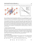
6.3.3. Lattice Diagram
The lattice diagram (also called bounce or reflection diagram) provides a convenient
graphical means for keeping track of the multiple wave reflections on the line. The general
lattice diagram is illustrated in Fig. 6.5. Each wave component is represented by a sloped
line segment that shows the time elapsed after the initial voltage change at the source as a
function of distance z on the line. For bookkeeping purposes, the value of the voltage
amplitude of each wave component is commonly written above the corresponding line
segment and the value of the accompanying current is added below. Starting with voltage
V
þ
1
¼ V
0
Z
0
=ðR
S
þ Z
0
Þ of the first wave component, the voltage amplitude of each
successive wave is obtained from the voltage of the preceding wave by multiplication with
the appropriate reflection coefficient
L
or
S
in accordance with Eq. (6.29). Successive
current values are obtained by multiplication with
L
or
S
, as shown in Eq. (6.30).
The lattice diagra m may be conveniently used to determine the voltage and current
distributions along the transmission line at any given time or to find the time response at
any given position. The variation of voltage and current as a function of time at a given
position z ¼ z
1
is found from the intersection of the vertical line through z
1
and the
sloped line segments representing the wave components. Figure 6.5 shows the first five
wave intersection times at position z
1
marked as t
1
, t
2
, t
3
, t
4
, and t
5
, respectively. At each
Figure 6.5 Lattice diagram for a lossless transmission line with unmatched terminations.
19 6 Weisshaar
© 2006 by Taylor & Francis Group, LLC
intersection time, the total voltage and current change by the amplitudes specified for the
intersecting wave component. The corresponding transient response for voltage and
current with R
S
¼ Z
0
=2 and R
L
¼ 5Z
0
corresponding to reflection coefficients
S
¼1=3
and
L
¼ 2=3, respectively, is shown in Fig. 6.6. The transient response converges to the
steady-state V
1
¼ 10=11 V
0
and I
1
¼ 2=11ðV
0
=Z
0
Þ, as indicated in Fig. 6.6.
6.3.4. A pplications
In many practical applications, one or both ends of a transmission line are matched to
avoid multiple reflections. If the source and/or the receiver do not provide a match,
multiple reflections can be avoided by adding an appropriate resistor at the input of the
line (source termination) or at the end of the line (end termination) [9,10]. Multiple
reflections on the line may lead to signal distortion including a slow voltage buildup or
signal overshoot and ringing.
Figure 6.6 Step response of a lossless transmission line at z ¼ z
1
¼ l=4 for R
S
¼ Z
0
=2 and
R
L
¼ 5Z
0
; (a) voltage response, (b) current response.
Tra n s m i s sion L i nes 197
© 2006 by Taylor & Francis Group, LLC
Over- and Under-driven Transmission Lines
In high-speed digital systems, the input of a receiver circuit typically presents a load to a
transmission line that is approximately an open circuit (unterminated). The step-voltage
response of an unterminated transmission line may exhibit a considerably different
behavior depending on the source resistance.
If the source resistance is larger than the characteristic impedance of the line, the
voltage across the load will build up monotonically to its final value since both reflection
coefficients are positive. This condition is refer red to as an underdriven transmission
line. The buildup time to reach a sufficiently converged voltage may correspond to
many round-trip times if the reflection coefficient at the source is close to þ1
(and
L
¼
oc
¼þ1), as illustrated in Fig. 6.7. As a result, the effective signal delay
may be several times longer than the delay time of the line.
If the source resistance is smaller than the characteristic impedance of the line, the
initial voltage at the unterminated end will exceed the final value (overshoot). Since the
source reflection coefficient is negative and the load reflection coefficient is positive,
the voltage response will exhibit ringing as the voltage converges to its final value. This
condition is referred to as an overdriven transmission line. It may take many round-trip
times to reach a sufficiently converged voltage (long settling time) if the reflection
coefficient at the source is close to 1 (and
L
¼
oc
An overdriven line can produce excessive noise and cause intersymbol interference.
Transmission-line Junctions
Wave reflections occur also at the junction of two tandem-connected transmission lines
encountered in practice. For an incident wave on line 1 with characteristic impedance Z
0,1
,
the second line with ch aracteristic impedance Z
0,2
presents a load resistance to line 1 that
is equal to Z
0,2
. At the junction, a reflected wave is generated on line 1 with voltage
reflection coefficient
11
given by
11
¼
Z
0,2
Z
0,1
Z
0,2
þ Z
0,1
ð6:34Þ
Figure 6.7 Step-voltage response at the termination of an open-circuited lossless transmission
line with R
S
¼ 5Z
0
ð
S
¼ 2=3Þ:
198 Weisshaar
© 2006 by Taylor & Francis Group, LLC
¼þ1Þ, as illustrated in Fig. 6.8.
having different characteristic impedances. This situation, illustrated in Fig. 6.9a, is often
Figure 6.9 Junction between transmission lines: (a) two tandem-connected lines and (b) three
parallel-connected lines.
Figure 6.8 Step-voltage response at the termination of an open-circuited lossless transmission line
with R
S
¼ Z
0
=5 ð
S
¼2=3Þ:
Tra n s m i s sion L i nes 199
© 2006 by Taylor & Francis Group, LLC
In addition, a wave is launched on the second line departing from the junction. The
voltage amplitude of the transmitted wave is the sum of the voltage amplitudes of
the incident and reflected waves on line 1. The ratio of the voltage amplitudes of the
transmitted wave on line 2 to the incident wave on line 1 is defined as the voltage
transmission coefficient
21
and is given by
21
¼ 1 þ
11
¼
2Z
0,2
Z
0,1
þ Z
0,2
ð6:35Þ
Similarly, for an incident wave from line 2, the reflection coefficient
22
at the junction is
22
¼
Z
0,1
Z
0,2
Z
0,1
þ Z
0,2
¼
11
ð6:36Þ
The voltage transmission coefficient
12
for a wave incident from line 2 and transmitted
into line 1 is
12
¼ 1 þ
22
¼
2Z
0,1
Z
0,1
þ Z
0,2
ð6:37Þ
If in addition lumped elements are connected at the junction or the transmission lines are
connected through a resistive network, the reflection and transmission coefficients will
change, and in general,
ij
1 þ
jj
[5].
For a parallel connection of multiple lines at a common junction, as illustrated in
characteristic impedances of all lines except for the line carrying the incident wave.
The reflection and transmission coefficients are then determined as for tandem connected
lines [5].
The wave reflection and transmission process for tandem and multiple parallel-
connected lines can be represented graphically with a lattice diagram for each line. The
complexity, however, is significantly increa sed over the single line case, in particular if
multiple reflections exist.
Reactive Terminations
In various transmission-line applications, the load is not purely resistive but has a reactive
component. Examples of reactive loads include the capacitive input of a CMOS gate, pad
capacitance, bond-wire inductance, as wel l as the reactance of vias, package pins, and
connectors [9,10]. When a transmission line is terminate d in a reactive element, the
reflected waveform will not have the same shape as the incident wave, i.e., the reflection
coefficient will not be a constant but be varying with time. For example, consider the step
response of a transmission line that is terminated in an uncharged capacitor C
L
. When the
incident wave reaches the termination, the initial response is that of a short circuit, and
the response after the capacitor is fully charged is an open circuit. Assuming the source
end is matched to avoid multiple reflections, the incident step-voltage wave is
v
þ
1
ðtÞ¼V
0
=2Uðt z=v
p
Þ. The voltage across the capacitor changes exponentially
from the initial voltage v
cap
¼ 0 (short circuit) at time t ¼t
d
to the final voltage
200 Weisshaar
© 2006 by Taylor & Francis Group, LLC
Fig. 6.9b, the effective load resistance is obtained as the parallel combination of the
v
cap
ðt !1Þ¼V
0
(open circuit) as
v
cap
ðtÞ¼V
0
1 e
ðtt
d
Þ=
ÂÃ
Uðt t
d
Þð6:38Þ
with time constant
¼ Z
0
C
L
ð6:39Þ
where Z
0
is the characteristic impedance of the line. Figure 6.10 shows the step-voltage
response across the capacitor and at the source end of the line for ¼ t
d
.
If the termination consists of a parallel combination of a capacitor C
L
and a resistor
R
L
, the time constant is obtained as the product of C
L
and the parallel combination of
R
L
and characteristic impedance Z
0
. For a purely inducti ve termination L
L
, the initial
response is an open circuit and the final response is a short circuit. The corresponding time
constant is ¼ L
L
=Z
0
.
In the general case of reactive terminations with mult iple reflections or with more
complicated source voltages, the boundary conditions for the reactive termination are
expressed in terms of a differential equation. The transient response can then be
determined mathematically, for example, using the Laplace transformation [11].
Nonlinear Terminations
For a nonlinear load or source, the reflected voltage and subsequently the reflection
coefficient are a function of the cumulative voltage and current at the termination
including the contribution of the reflected wave to be determined. Hence, the reflection
coefficient for a nonlinear termination cannot be found from only the termination
characteristics and the characteristic impedance of the line. The step-voltage response for
each reflection instance can be determined by matching the I–V characteristics of the
termination and the cumulative voltage and current characteristics at the end of the
transmission line. This solution process can be constructed using a graphical technique
known as the Bergeron method [5,12] and can be implemented in a computer program.
Figure 6.10 Step-voltage response of a transmission line that is matched at the source and
terminated in a capacitor C
L
with time constant ¼ Z
0
C
L
¼ t
d
.
Tra n s m i s sion L i nes 201
© 2006 by Taylor & Francis Group, LLC
Time-Domain Reflectometry
Time-domain reflectometry (TDR) is a measurement technique that utilizes the infor-
mation contained in the reflected waveform and observed at the source end to test,
characterize, and model a transmission-line circuit. The basic TDR principle is illustrated
in Fig. 6.11. A TDR instrument typically consists of a precision step-voltage generator
with a known source (reference) impedance to launch a step wave on the transmission-line
circuit under test and a high impedance probe and oscilloscope to sample and display the
voltage waveform at the source end. The source end is generally well matched to establish
a reflection-free reference. The voltage at the input changes from the initial incident
voltage when a reflected wave generated at an impedance discontinuity such as a change in
line impedance, a line break, an unwanted parasitic reactance, or an unmatched
termination reaches the source end of the transmission line-circuit.
The time elapsed between the initial launch of the step wave and the observation of
the reflected wave at the input corresponds to the round-trip delay 2t
d
from the input to
the location of the impedance mismatch and back. The round-trip delay time can be
converted to find the distance from the input of the line to the location of the impedance
discontinuity if the propagation velocity is known. The capability of measuring distance is
used in TDR cable testers to locate faults in cables. This measurement approach is
particularly useful for testing long, inaccessible lines such as underground or undersea
electrical cables.
The reflected waveform observed at the input also provides information on the type
for several common transmission-line discontinuities. As an example, the load resistance in
the circuit in Fig. 6.11 is extracted from the incident and reflected or total voltage observed
at the input as
R
L
¼ Z
0
1 þ
1
¼ Z
0
V
total
2V
incident
V
total
ð6:40Þ
where ¼ V
reflected
=V
incident
¼ðR
L
Z
0
Þ=ðR
L
þ Z
0
Þ and V
total
¼ V
incident
þ V
reflected
.
Figure 6.11 Illustration of the basic principle of time-domain reflectometry (TDR).
202 Weisshaar
© 2006 by Taylor & Francis Group, LLC
of discontinuity and the amount of impedance change. Table 6.2 shows the TDR response
The TDR principle can be used to profile impedance changes along a transmission
line circuit such as a trace on a printed-circuit board. In general, the effects of multiple
reflections arising from the impedance mismatches along the line need to be included to
extract the impedance profile. If the mismatches are small, higher-order reflections can be
ignored and the same extraction approach as for a single impedance discontinuity
can be applied for each discontinuity. The resolution of two closely spaced discontinuities,
however, is limited by the rise time of step voltage and the overall rise time of the
TDR system. Further information on using time-domain reflectometry for analyzing and
modeling transmission-line systems is given e.g. in Refs. 10,11,13–15.
Table 6.2 TDR Responses for Typical Transmission-line Discontinuities.
TDR response Circuit
Tra n s m i s sion L i nes 203
© 2006 by Taylor & Francis Group, LLC
6.4. SINUSOIDAL STEADY-STATE RESPONSE
OF TRANSMISSION LINES
The steady-state response of a transmission line to a sinusoidal excitation of a given
frequency serves as the fundamental solution for many practical transmission-line
applications including radio and television broadcast and transmission-line circuits
operating at microwave frequencies. The frequency-domain information also provides
physical insight into the signal propagation on the transmission line. In particular,
transmission-line losses and any frequency dependence in the R, L, G, C line parameters
can be readily taken into account in the frequency-domain analysis of transmission lines.
The time-domain response of a transmission-line circuit to an arbitrary time-varying
excitation can then be obtained from the frequency-domain solution by applying the
concepts of Fourier analysis [16].
As in standard circuit analysis, the time-harmonic voltage and current on the
transmission line are conveniently expressed in phasor form using Euler’s identity
e
j
¼ cos þj sin . For a cosine reference, the relations between the voltage and current
phasors, V(z) and I(z), and the time-harmonic space–time-depend ent quantities, vðz, tÞ and
i ðz, tÞ, are
vðz, tÞ¼RefVðzÞe
j!t
g
ð6:41Þ
i ðz, tÞ¼RefIðzÞe
j!t
g
ð6:42Þ
The voltage and current phasors are functions of position z on the transmission line and
are in general complex.
6.4.1. Characte rist ic s o f Lossy Tran s mission Line s
The transmission-line equations, (general telegrapher’s equations) in phasor form for a
general lossy transmission line can be derived directly from the equivalent circuit for a
short line section of length Áz ! 0 shown in Fig. 6.12. They are
dVðzÞ
dz
¼ðR þ j!LÞIðzÞ
ð6:43Þ
dIðzÞ
dz
¼ðG þj!CÞVðzÞ
ð6:44Þ
Figure 6.12 Equivalent circuit model for a short section of lossy transmission line of length Áz
with R, L, G, C line parameters.
204 Weisshaar
© 2006 by Taylor & Francis Group, LLC
The transmission-line equations, Eqs. (6.43) and (6.44) can be combined to the complex
wave equation for voltage (and likewise for current)
d
2
VðzÞ
dz
2
¼ðR þ j!LÞðG þj!CÞVðzÞ¼
2
VðzÞð6:45Þ
The general solution of Eq. (6.45) is
VðzÞ¼V
þ
ðzÞþV
ðzÞ¼V
þ
0
e
z
þ V
0
e
þz
ð6:46Þ
where is the propagation constant of the transmission line and is given by
¼ þj ¼
ffiffiffiffiffiffiffiffiffiffiffiffiffiffiffiffiffiffiffiffiffiffiffiffiffiffiffiffiffiffiffiffiffiffiffiffiffiffiffiffiffi
ðR þ j!LÞðG þj!CÞ
p
ð6:47Þ
and V
þ
0
¼jV
þ
0
je
j
þ
and V
0
¼jV
0
je
j
are complex constants. The real time-har monic
voltage waveforms vðz, tÞ corresponding to phasor V(z) are obtained with Eq. (6.41) as
vðz, tÞ¼v
þ
ðz, tÞþv
ðz, tÞ
¼jV
þ
0
je
z
cosð!t z þ
þ
ÞþjV
0
je
z
cosð!t þz þ
Þ
ð6:48Þ
The real part of the propagation constant in Eq. (6.47) is known as the attenuation
constant measured in nepers per unit length (Np/m) and gives the rate of exponential
attenuation of the voltage and current amplitudes of a traveling wave.* The imaginary
part of is the phase constant ¼ 2= measured in radians per unit length (rad/m), as in
the lossless line case. The corresponding phase velocity of the time-harmonic wave is
given by
v
p
¼
!
ð6:49Þ
which depends in general on frequency. Transmission lines with frequency-dependent
phase velocity are called dispersive lines. Dispersive transmission lines can lead to signal
distortion, in particular for broadband signals.
The current phasor I(z) associated with voltage V(z) in Eq. (6.46) is found with
Eq. (6.43) as
IðzÞ¼
V
þ
Z
0
e
z
V
Z
0
e
þz
ð6:50Þ
*The amplitude attenuation of a traveling wave V
þ
ðzÞ¼V
þ
0
e
z
¼ V
þ
0
e
z
e
jz
over a distance l can
be expressed in logarithmic form as ln jV
þ
ðzÞ=V
þ
ðz þ lÞj ¼ l (nepers). To convert from the
attenuation measured in nepers to the logarithmic measure 20 log
10
jV
þ
ðzÞ=V
þ
ðz þ lÞj in dB, the
attenuation in nepers is multiplied by 20 log
10
e 8:686 (1 Np corresponds to about 8.686 dB). For
coaxial cables the attenuation constant is typically specified in units of dB/100 ft. The conversion to
Np/m is 1 dB/100 ft 0.0038 Np/m.
Transmission Lines 205
© 2006 by Taylor & Francis Group, LLC
and are illustrated in Fig. 6.13.
The quantity Z
0
is defined as the characteristic impedance of the transmission line and is
given in terms of the line parameters by
Z
0
¼
ffiffiffiffiffiffiffiffiffiffiffiffiffiffiffiffiffiffi
R þ j!L
G þj!C
s
ð6:51Þ
As seen from Eq. (6.51), the characteristic impedance is in general complex and frequency
dependent.
The inverse expressions relating the R, L, G, C line parameters to the characteristic
impedance and propagation constant of a transmission line are found from Eqs. (6.47) and
(6.51) as
R þj!L ¼ Z
0
ð6:52Þ
G þj!C ¼ =Z
0
ð6:53Þ
Figure 6.13 Illustration of a traveling wave on a lossy transmission line: (a) wave traveling in þz
direction with
+
¼0 and ¼1/(2 ) and (b) wave traveling in z direction with
¼60
and
¼1/(2 ).
206 Weisshaar
© 2006 by Taylor & Francis Group, LLC
These inverse relationships are particularly useful for extracting the line parameters
from experimentally determined data for characteristic impedance and propagation
constant.
Special Cases
For a lossless line with R ¼0 and G ¼0, the propagation constant is ¼ j!
ffiffiffiffiffiffiffi
LC
p
.
The attenuation constant is zero and the phase velocity is v
p
¼ != ¼ 1=
ffiffiffiffiffiffiffi
LC
p
. The
characteristic impedance of a lossless line is Z
0
¼
ffiffiffiffiffiffiffiffiffiffi
L=C
p
, as in Eq. (6.14).
In general, for a lossy transmission line both the attenuation constant and the phase
velocity are frequency dependent, which can give rise to signal distortion.* However, in
many practical applica tions the losses along the trans mission line are small. For a low loss
line with R !L and G !C, useful approximate expressions can be derived for the
characteristic impedance Z
0
and propagation constant as
Z
0
ffiffiffiffi
L
C
r
1 j
1
2!
R
L
G
C
!
ð6:54Þ
and
R
2
ffiffiffiffi
C
L
r
þ
G
2
ffiffiffiffi
L
C
r
þ j!
ffiffiffiffiffiffiffi
LC
p
ð6:55Þ
The low-loss conditions R !L and G !C are more easily satisfied at higher
frequencies.
6.4.2. Terminated Transmission lines
If a transmission line is terminated with a load impedance that is different from the
characteristic impedance of the line, the total time-harmonic voltage and current on
the line will consist of two wave components traveling in opposite directions, as given
by the general phasor expressions in Eqs. (6.46) and (6.50). The presence of the two
wave components gives rise to standing waves on the line and affects the line’s input
impedance.
Impedance Transformation
L
In the steady-state an alysis of transmission-line circuits it is expedient to measure distance
on the line from the termination with known load impedance. The distance on the line
from the termination is given by z
0
. The line voltage and current at distance z
0
from the
*For the special case of a line satisfying the condition R =L ¼ G=C, the characteristic impedance
Z
0
¼
ffiffiffiffiffiffiffiffiffiffi
L=C
p
, the attenuation constant ¼ R=
ffiffiffiffiffiffiffiffiffiffi
L=C
p
, and the phase velocity v
p
¼ 1=
ffiffiffiffiffiffiffi
LC
p
are
frequency independent. This type of line is called a distortionless line. Except for a constant signal
attenuation, a distortionless line behaves like a lossless line.
Tra n s m i s sion L i nes 207
© 2006 by Taylor & Francis Group, LLC
Figure 6.14 shows a transmis sion line of finite length terminated with load impedance Z .
termination can be related to voltage V
L
¼ Vðz
0
¼ 0Þ and current I
L
¼ Iðz
0
¼ 0Þ at the
termination as
Vðz
0
Þ¼V
L
cosh z
0
þ I
L
Z
0
sinh z
0
ð6:56Þ
Iðz
0
Þ¼V
L
1
Z
0
sinh z
0
þ I
L
cosh z
0
ð6:57Þ
where V
L
=I
L
¼ Z
L
. These voltage and current transformations between the input and
output of a transmission line of lengt h z
0
can be conveniently expressed in ABCD matrix
form as*
Vðz
0
Þ
Iðz
0
Þ
!
¼
AB
CD
!
Vð0Þ
Ið0Þ
!
¼
coshðz
0
Þ Z
0
sinhðz
0
Þ
ð1=Z
0
Þsinhðz
0
Þ coshðz
0
Þ
!
Vð0Þ
Ið0Þ
!
ð6:58Þ
The ratio Vðz
0
Þ=Iðz
0
Þ defines the input impedance Z
in
ðz
0
Þ at distance z
0
looking toward
the load. The input impedance for a general lossy line with characteristic impedance Z
0
and terminated with load impedance Z
L
is
Z
in
ðz
0
Þ¼
Vðz
0
Þ
Iðz
0
Þ
¼ Z
0
Z
L
þ Z
0
tanh z
0
Z
0
þ Z
L
tanh z
0
ð6:60Þ
It is seen from Eq. (6.60) that for a line terminated in its characteristic impedance
(Z
L
¼ Z
0
), the input impedance is identical to the characteristic impedance, independent
of distance z
0
. This property serves as an alternate definition of the characteristic
impedance of a line and can be applied to experimentally determine the characteristic
impedance of a given line.
The input impedance of a transmission line can be used advantageously to determine
the voltage and current at the input terminals of a transmission-line circuit as well as the
average power delivered by the source and ultimately the average power dissipated in
the load. 6.15 shows the equivalent circuit at the input (source end) for the
in
and current I
in
are easily
*The ABCD matrix is a common representation for two-port networks and is particularly useful for
cascade connections of two or more two-port networks. The overall voltage and current
transformations for cascaded lines and lumped elements can be easily obtained by multiplying the
corresponding ABCD matrices of the individual sections [1]. For a lossless transmission line, the
ABCD parameters are
AB
CD
!
lossless line
¼
cos jZ
0
sin
ðj=Z
0
Þsin cos
!
ð6:59Þ
where ¼ z
0
is the electrical length of the line segment.
208 Weisshaar
© 2006 by Taylor & Francis Group, LLC
Figure
transmission-line circuit in Fig. 6.14. The input voltage V
determined from the voltage divider circuit. The average power delivered by the source to
the input terminals of the transmission line is
P
ave, in
¼
1
2
RefV
in
I
in
gð6:61Þ
The average power dissipated in the load impedance Z
L
¼ R
L
þ jX
L
is
P
ave, L
¼
1
2
RefV
L
I
L
g¼
1
2
jI
L
j
2
R
L
¼
1
2
V
L
Z
L
2
R
L
ð6:62Þ
where V
L
and I
L
can be determined from the inverse of the ABCD matrix transformation
Eq. (6.58).* In general, P
ave, L
< P
ave, in
for a lossy line and P
ave, L
¼ P
ave, in
for a lossless
line.
Example. Consider a 10 m long low-loss coaxial cable of nominal characteristic
impedance Z
0
¼ 75 , attenuation constant ¼ 2:2 dB per 100 ft at 100 MHz, and
velocity factor of 78%. The line is terminated in Z
L
¼ 100 , and the circuit is
operated at f ¼100 MHz. The ABCD parameters for the transmission line are
A ¼D ¼0:1477þj0:0823, B¼ð0:9181þj74:4399Þ, and C ¼ð0:0002þj0:0132Þ
1
.
The input impedance of the line is found as Z
in
¼ð59:3þj4:24Þ. For a so urce voltage
jV
S
j¼10V and source impedance Z
S
¼75, the average power delivered to the input of
the line is P
ave,in
¼164:2mW and the average power dissipated in the load impedance is
P
ave,L
¼138:3mW. The difference of 25.9mW (16% of the input power) is dissipated in
the transmission line.
Figure 6.14 Transmission line of finite length terminated in load impedance Z
L
.
Figure 6.15 Equivalent circuit at the input of the transmission line circuit shown in Fig. 6.14.
*The inverse of Eq. (6.58) expressing the voltage and current at the load in terms of the input voltage
and current is
V
L
I
L
!
¼
D B
CA
!
V
in
I
in
!
ð6:63Þ
Tra n s m i s sion L i nes 209
© 2006 by Taylor & Francis Group, LLC