MOSFET MODELING FOR VLSI SIMULATION - Theory and Practice Episode 5 ppsx
Bạn đang xem bản rút gọn của tài liệu. Xem và tải ngay bản đầy đủ của tài liệu tại đây (1.6 MB, 40 trang )
136
4
MOS
Capacitor
ACCUMULATION
METAL
OXIDE
HOLE
DENSITY
Ec
Ei
EfP
__
_____
00"
00
E"
(a)
L-4
fox
p-TYPE
SILICON
tg
X
INVERSION
Ef,
Fig.
4.10
Effect of applied voltage on a p-type
MOS
capacitor; (a) negative voltage
V,,
=
(V,
-_
yfb)
causes hole accumulation at the surface;
(b)
positive voltage depletes holes
from
the silicon surface; and (c) a large positive
V,,
causes inversion,
forming
an n-type
layer at the silicon surface
charged acceptor ions. In other words, a positive charge on the gate induces
a negative charge
Q,
at the silicon surface. Since holes are depleted at the
surface it is referred
to
as the
depletion
condition. This is analogous to the
depletion region in
pn
junctions discussed in section
2.5.
Since hole
concentration decreases at the surface, we see from
Eq.
(4.15)
that
(Ei
-
Ef)
4.2
MOS
Capacitor
at
Non-Zero
Bias
137
must decrease resulting in
Ei
coming closer to
E,
thereby bending the
bands downward near the surface (Figure 4.10b). Thus in
vg
’
vfb
depletion
4s
>O,
(4.22)
Let us now calculate the depletion layer charge. The band bending potential
4(x)
must satisfy Poisson’s equation (2.41) and is used to calculate the
induced charge
Q,
within the space charge region of width
X,
at the surface,
also called the depletion width. We refer to this induced charge in the
depletion region as the
bulk
charge
denoted by Qb. Applying Gauss’ law
we have [cf. Eq. (4.18)]
Q,
=
Q,(depletion)
=
-
E~E,~€,~
(F/cm2). (4.23)
Under the depletion approximation (cf. section 2.5.2)
n
=
p
=
0
(no free
carriers) and the assumption that the substrate is p-type (uniform concentra-
tion N, cm-
’)
so
that No(
=
Nb)
>>
N,, the Poisson equation (2.41) becomes
I
Q,
<O.
(4.24)
Integrating the above equation twice from the interface
(x
=
0) to the
depletion edge
(x
=
X,)
and using the boundary conditions
4=4,
and
-=-&si
d4
at
x=O
(4.25a)
dx
and
d4
dx
4=-=O
at
x=x,
we get
(4.2
5
b)
(4.26)
which gives a relationship between the band bending and the surface
potential. The depletion width
X,
in the above equation can easily be
calculated by substituting
Eq.
(4.26) in (4.24) giving
(4.27)
138
4
MOS
Capacitor
Note that the depletion width given by the equation above is the same as
that obtained for one sided step
pn
junction under the depletion approxima-
tion [cf. Eq. (2.53)]. This shows that
we can treat the silicon surface/silicon
bulk
system as
a
one sided step junction.
The depletion or bulk charge
Qb
can now be obtained from Eq. (4.23) using
Eqs. (4.26) and (4.27) giving
Q
b-
-
-
E
0
E
SI
.€
SI
.
=
E
0
E
sidch1
=
-
J-
(F/cm2). (4.28)
Alternatively,
Qb
can also be obtained by integrating the charge
qNb
under
the depletion width
X,
giving
dx
x=o
(4.29)
where we have made use of Eq. (4.27) for
X,.
For n-type silicon,
Qb,
given by
Eq. (4.29), is a positive quantity.
Note that Eq. (4.27) for
X,
is in terms of surface potential
$s.
Since
$s
itself
is a function of gate voltage
V,
[cf. Eq. (4.20)], one can also write
X,
in
terms
of
V,.
Thus, by substituting
$s
from Eq. (4.27) and
Qs(
=
Qb)
from
Eq. (4.29) in Eq. (4.20) and solving the resulting quadratic equation in
X,
we get, under the depletion approximation
:ox
\v
EOEsiqNb
(4.30)
Equation (4.30) shows that when
V,
=
Vfb,
the depletion width
X,
=
0,
consistent with the definition of the flat band voltage.
4.2.3
Inversion
If we continue to increase the positive gate voltage
V,,(
=
V,
-
V,,),
the
downward band bending would further increase. In fact, a sufficiently large
voltage can cause
so
much band bending that it may cause the midgap
energy
Ei
to cross over the constant Fermi level
E,
i.e.
E,
>
Ei.
When this
happens the surface behaves like n-type material with an electron concentra-
tion given by Eq.
(2.10a).
Note that this n-type surface is formed not by
doping but instead by
inversion
of the original p-type substrate due to the
applied gate voltage. This is referred to as the
inversion
condition and is
4.2
MOS
Capacitor at
Non-Zero
Bias
139
shown in Figure 4.10~. Thus in
Vg
>>
Vfbj
inversion
4,
>O,
(4.3
1)
The surface is inverted as
soon
as
E,
>
Ej.
This is called the weak inversion
regime
because the electron concentration remains small until
E,
is
considerably above
Ei.
If
we further increase
Vg,,
the concentration
of
electrons at the surface will equal, and then exceed, the concentration
of
the holes in the substrate. This
is
called the strong inversion regime.
One may ask, where these electrons (minority carriers) in the p-substrate
come from when inversion sets in. Physically speaking these electrons come
from the electron-hole generation, within the space charge (depletion)
region, caused by the thermal vibration
of
lattice phonons. The rate of
thermal generation depends upon the minority carrier life time
zo
which
is typically in pec (lO-%ec). This means that minority carriers are not
immediately available when an inverting gate voltage is applied. The time
tin"
required to form an inversion layer at the surface is approximated by
r
Q,
<O.
c141
(4.32)
where
ni
is the intrinsic carrier concentration. For a typical value
of
z,,
=
1
psec and
N,
=
lOI5
~m-~, tin"
-
0.2
sec. Thus the formation
of
the
inversion layer is a relatively
slow
process compared
to
the time required
for the holes (majority carriers) topow from
or
to the silicon surface which
is
of
the order of picoseconds (i.e. the dielectric relaxation time associated
with the substrate.)
The inversion layer is important from the
MOS
transistor operation point
of
view. It
is
the nature of the inversion layer, that is, number of carriers
in the inversion layer (i.e. inversion layer charge
Qi),
the mobility
of
the carriers in the layer etc. which determines the current in the transistor.
The inversion layer charge
Qi
can be calculated by including the electron
concentration
n
in Poisson's equation (4.24). Let us first calculate n.
Rewriting Eq. (4.4) as
ni
=
N,e-4flvt
and substituting
ni
in Eq.
(2.10)
we get
n
=
Nbe(@-2#'f)/Vc.
(4.33a)
and
p
=
N
e-6'lvt
(4.33b)
140 4
MOS
Capacitor
At the surface
4
=
4s
and therefore, from
Eq.
(4.33a), the electron concen-
tration
n,
at the surface
is
given by
(4.34)
When
4,
=
4f,
i.e.
Ei
=
E,,
we see that
n,
=
ni.
That is, the silicon becomes
intrinsic. ‘When
4s
>
g5f,
we have
E,
>
Ei and the surface is inverted. At
the onset
of
weak inversion the surface potential
4,
is slightly larger than
4f
and in this case the depletion width is given by
Eq.
(4.27). As we further
increase
4,
by increasing the gate voltage
V,,
the depletion width
X,
widens
and the electron concentration
n,
at the surface increases (see
Eq.
4.34).
When the gate voltage is such that 4,=24,,
n,=
N,,
i.e.,
the electron
concentration at the surface becomes equal to the hole concentration in
the bulk.
When this happens the surface is said to be strongly inverted, and
under this condition, the depletion width reaches its maximum value
Xdn,,
which can be obtained by replacing
$s
=
24,
in
Eq.
(4.27).
Thus,
n
sb
=
N
e(4”-24f)/vt.
(4.35)
The condition
4,
=
24,
is often referred to as the
classical condition
for
strong inversion.
When
4,
>
24,,
the depletion width increases but very
slowly. This is because the inversion charge immediately adjacent to the
oxide-silicon interface shields the interior (bulk) of the semiconductor from
any additional charge on the gate.
-
1.4
‘5
N~~~=Q~
/q=1~’3cm2
0-
N,
=to’5cm‘3
T
=L*2OK
Oo
0
10
20
30
DISTANCE
FROM
SURFACE,X
(A)
0
Fig.
4.11 Calculated electron concentration
in
silicon (100) and (111) surface as a
function of distance from the surface for classical and quantum case.
(From
Stern and
Howard
[IS])
4.2
MOS
Capacitor at Non-Zero
Bias
141
The thickness of the inversion layer has been calculated using both quantum
mechanical and classical approaches. These calculation show
[
15,161 that
theo average “inversion layer thickness” at room temperature is about
50
A,
depending on the substrate doping concentration and gate voltage.
Although not important from a circuit modeling point of view, it is
interesting to consider the differences in the charge distributions calculated
using the two approaches. The differences are, as shown in Figure 4.11, in
two aspects.
In the classical case, the electron density has its maximum value at the
oxide-silicon interface, and it decreases steadily as we move from the
surface into the bulk.
In
the quantum mechanical case, the electron
density is zero
at
the interface, increases to its maximum value, and then
decreases with the distance from the surface.
In the classical case, the electron distribution is independent
of
the crystal
orientation while it depends on the crystal orientation in the quantum
mechanical case.
Figure
4.1
1
also
shows that most
of
the electrons are confined in
a
layer 50
A
thick. For this reason, the motion of the electrons in the channel of
a
MOSFET
can be regarded
as
two-dimensional, provided device width and
length are not very small (cf. section 3.7.7).
We will now return to calculate the inversion layer charge density
Qi.
Including the electron concentration
n
from
Eq.
(4.33) in Poisson’s equation
(4.24) yields
(4.36)
Integrating once under the boundary conditions (4.25) we get7
’
Multiplying both sides
of
the Poisson’s equation
by Z(d+/dx)
and using the identity,
Eq. (4.36) becomes
which can easily be integrated to give (4.37).
142
4
MOS
Capacitor
Using Gauss’ theorem, we get the induced charge density
Q,
in the silicon
as
[cf.
Eq.
(4.18)]
Qs
=
-
EOEsigsi
=
-
Jm
~4,
+
Ke(4.
24f)/vt1
(C/cm’)
(4.38)
which could further be simplified to
Q,
=
-
JWr4,
+
~~e(+s-2~f)/~~1~/~ (C/cm’) (4.39)
where we have dropped
-
1
after the
e4s’vt
term because the exponential
term is
so
large in strong inversion that
-
1
makes no difference, and in
weak inversion the term
Vte(4sp24f)ivt
is
so
small that the entire minority
carrier term can be neglected. Note that this induce charge
Q,
is the sum
of
the inversion charge
Qi
and depletion charge
Qb,
that is
Qs
=
Qi
+
Qb.
21
I
I
I
I
I
to,
=
300
15
-3
Nb
=
5x10
cm
UI
dI
II
g
(4.40)
-
-
2
3
a:
W
-
n
(3
a
a
1
V
W
Qb
.
-
I
1
0.9
0
0
-3
0.4
0.5
0.6
0.7
0.8
SURFACE POTENTIAL, (V)
Fig. 4.12 Variation
of
inversion layer charge density
Qi
[Eq.
(4.41)],
bulk
charge density
Qh
[Eq.
(4.29)], and the total semiconductor charge density
Q,(
=
Qb
+
Qi)
[Eq.
(4.39)] versus
surface potential
ds
in all regimes
of
device operation
for
a p-type substrate,
N,
=
5.1015
cm-
’,
to,
=
300
A,
and
V,,
=
0
V
4.2
MOS
Capacitor at Non-Zero Bias
143
Using
Eq.
(4.29)
for
Qb
and
Eq.
(4.39)
for
Q,,
we get the inversion charge
Qi
from
Eq.
(4.40)
as
Qi
=
-
,/-[,/4,
+
Vte(4s-2$f)'"t
-
A]
(C/cm2).
(4.41)
This gives the relationship between the inversion charge density
Qi
and the
surface potential
4,.
Figure
4.12
shows various charges as a function
of
4,.
Note that the depletion charge
Qb
does not vary appreciably.
Also
note
that
Qi
and
Q,
have two distinct regions, which become more apparent when
plotted on a logarithmic scale as shown in Figure 4.13a, where
Qi
is plotted
as a function
of
4s.
These regions are (a)
weak inversion
and (b)
strong
inversion.
Classically, the condition
4,
=
24,.
separates the region between
the weak and strong inversion. Often, however, the inversion regime is
divided into three regions; the third region which lies between the weak
and strong inversion is called
moderate inversion,
defined as the region
between
24,.
and
24,.
+
6Vt
(see Figure 4.13b). In this scheme the region
beyond
24,.
+
67/,
is the strong inversion region
[IS].
Weak Inversion.
Weak inversion sets in when the surface band bending is
4,.
and it extends to
24r
(see Fig.
4.13).
Within this region, the inversion-
layer charge
Qi
is small compared to the depletion-layer charge
Qb,
that is
I
Qi
I
<<
I
Qb
I
(weak-inversion).
(4.42)
I
04r
5
Id"
>
0.5
0.7
0.9
1.1
SURFACE
POTENTIAL, ps(V 1
r
0.5
0.7
0.9
1.1
SURFACE
POTENTIAL,$,CV
1
(a)
(b)
Fig.
4.13
Variation
of
inversion layer charge density
Qi
versus surface potential
4s
for
p-type substrate. (a) showing weak and strong region
of
operation (b) three different
regimes
of
inversion; weak, moderate and strong inversion.
N,
=
5.1015
CIT-~,
to,
=
300A
and
V,,
=
OV
144 4
MOS
Capacitor
For a small
4s,
Eq.
(4.41) could be simplified* by assuming that the
exponential term is small compared to
4s,
resulting in the following
expression for
Qi
EE.
N
Vte(bs-
2bf)/“t (weak-inversion) (C/cm2).
(4.43)
Thus,
in the weak inversion regime
Qi
is essentially an exponential function
of
the surface potential
4,.
This is plotted as a dashed line in Figure 4.13a.
Strong Inversion.
Strong inversion is defined by the condition that the
inversion layer charge
Qi
is
large compared to the depletion region charge
Qb,
i.e.
1
Qi
I
>
I
Q,
I
(strong-inversion). (4.44)
Here the exponential term in
Eq.
(4.41) is large compared to
4s
and thus
Qi
in strong inversion becomes
Q~
=
.J2E,t,iqN,I:
e4JZVt
(strong-inversion) (C/cmZ)). (4.45)
The inversion layer charge is an exponential function of the surface potential
with a slope of
1/2V1
(on a log scale). Therefore,
a small increment of the
surface potential induces a large change in the inversion
layer
charge.
Using
Eq.
(4.39) for
Q,
in
Eq.
(4.20) we get a relationship between the gate
voltage and surface potential as
This is an implicit relation in
+s
and must be solved numerically (see
Appendix
E).
The result of such simulations are shown in Figure 4.14.
At
low gate voltage
(>
V,.,)
4s
increases reasonably rapidly with gate bias and
so
does the depletion width
X,
under the gate. This regime corresponds
to the depletion and weak inversion regions of the device operation. At
larger gate biases,
$s
hardly changes;
4s
has become pinned. The classical
condition for the pinning is
+,=24,
This pinning occurs when strong
inversion sets in. The condition when this happens is often called the
condition for
threshold
and the corresponding gate voltage is called
thre-
shold voltage
Vth.
It
is one of the important device parameter which will
be discussed in more details in Chapter
5.
Using the Binomial theorem
terms
we
have
fi
=
1
+
x/2
=
1
+
x/2
-
x2/8
+
and retaining the first two
4.2
MOS
Capacitor at Non-Zero Bias
145
1.0.
,
,
,
I
I
Ill1
to,
=
300
8
N,
=
i
x
10'6~m3
b
-
-
0.0
IIlI,IIII
0.0
0.L
0.8
1.2
1-6
2.0
GATE VOLTAGE,Vq
(V)
Fig. 4.14 Variation of surface potential
q5s
with gate voltage
V,
obtained using
Eq.
(4.46).
N,
=
1.0
x
lOI6
cm-
',
to,
=
300
A,
V,,
=
OV.
Cross indicates
dS
=
24,
point which separate
weak and strong inversion region
To
summarize, we have calculated separate expressions for the induced
charge
Q,
that are valid in the depletion
[Qb,
Eq.
(4.29)] and inversion
[Qi,
Eq.
(4.41)] regime
of
MOS
capacitor operation. However, one can easily
derive
a
general expression for
Q,
that is valid for all the regimes of device
operation by including both the holes and electrons and thus solving the
Poisson
Eq.
(2.41). Using
Eqs.
(4.33) for
n
and
p
and noting that in the
bulk charge neutrality dictates that
N,
-
N,
=
npo
-
ppo,
npo
and
ppo
being
the carrier density in the bulk
(ppo
%
Nb
and
npo
z
Nbe-2'fiVt),
the Poisson
Eq.
(2.41) becomes
dx2
E~E,(
d2Q,
-
qNb
[I
+
,(+-2+f)/Vr
-
e-4ivt
-
e-26fivtl
for
01
x
5
x,.
(4.47)
Integrating the above equation, under the boundary condition (4.25), results
in the following expression for
Q,
which includes both holes and electrons
1613
c121,
Q,
=
-
J2E,E,iqN,[4,
+
e-2$fiVt(Vre$JVt
-
Vr
-
4s)
+
Vre-@J"t
-
~~1''~
(C/cm2). (4.48)
The charge expression (4.48) is valid in all the regions
of
MOS
capacitor
operation-accumulation, depletion, and inversion. It should be pointed
out that in the literature
Eq.
(4.48) is also written in terms
of
npo
and
ppo
146
4
MOS
Capacitor
INVERSION
ACCUMULATION
'DEPLETION
-9
'-0:2
'
:O
012
'
0:4
'
d.6
'
Ol8
IlO
SURFACE POTENTIAL,
pSC
V
>
Fig. 4.15 Variation of the induced charge density
Q,
in silicon versus surface potential
q5s
for p-type substrate in all regimes
of
device operation obtained using
Eq.
(4.48).
N,
=
5
x
10'5cm-3,
to,
=
300A
and
Vfb
=
OV
where
L,
is the Debye length defined as
(4.50)
and the ratio
n,,/p,,
=
VIec24fi"t.
Equations (4.29) and (4.41) are special
cases
of
Eq.
(4.48).
The variation
of
the induced charge
Q,
as
a
function
of
4,
using Eq. (4.48) for p-type substrate is illustrated in Figure 4.15 which
clearly shows all the three regimes
of
operation. These regimes are easily
identified:
When
4s
<
0,
the
MOS
structure is in the accumulation mode. The term
that predominates in Eq. (4.48) is
e-4s/vt
and therefore in this regime
Q,
varies as
Q,
-
ec4s/2vt
(accumulation).
(4.5
1
a)
4.3
Capacitance
of
MOS
Structures
147
Table
4.2.
Definition of silicon surface parameters
-
+
P
Accumulation
-
Depletion/lnversion
+
n
Accumulation
+
Depletion/Inversion
-
+
+
-
-
-
+
b
When
4s
>
0
such that
0
<
4,
<
24
f,
the structure is in the depletion and
weak inversion regime. In this case the term that predominates in
Eq.
(4.48) is
6
and therefore
Q,
varies as
Q,
-
,,/& (depletion and weak inversion). (4.5 1 b)
b
When
4s
>
24
f,
the structure is in the strong inversion mode. The
Q,
-
e4s/2Vt
(strong inversion). (4.51~)
Note that the accumulation, depletion and inversion conditions described
by
Eqs.
(4.21), (4.22), and (4.31) are for p-type substrates. However, for
n-type substrates these conditions will be reversed as shown in Table 4.2.
predominant term in
Q,
varies as
4.3
Capacitance
of
MOS
Structures
In the previous section we developed relationships between the charge and
potential under different gate voltage conditions across a
MOS
capacitor.
Now we will see how the capacitance of the
MOS
system varies with the
applied voltage. The capacitance
of
any system is the ratio of the variation
in charge to the corresponding variation in the small-signal applied voltage.
Thus the capacitance
C,
of
a
MOS
structure is
Substituting the value of
V,,
from
Eq.
(4.19)
in
Eq.
(4.16) we get
Q
cox
v,
=
(Dms
+
4,
+
L.
Since
QmS
is a constant, it follows that
(4.52)
(4.53)
148
4
MOS
Capacitor
dQ
d4S
C,
=
-
2
Combining Eqs.
(4.52)
and
(4.53)
gives the capacitance of an
MOS
system as
(F/cm2)
(
F/cm2).
Rearranging
Eq.
(4.17)
and differentiating with respect to
4,
we get
11 1
C,
C,,
dQ,ld4,
__
dQ,
1
-
dQ, dQ,
d4s
d4s
d4s
+-
-
(4.54)
(4.55)
The quantity
-
dQs/d4, can be interpreted as the capacitance per unit area,
C,
associated with the silicon depletion or space charge region, i.e.
(4.56)
and, can easily be obtained by differentiating Eq.
(4.48)
giving the follow-
ing expression for
C,
mEOEsi
[1
-
e-4./vt
+
e-29f/Vc(,9./vt
-
I)]
2[l/,e-9s/vr
+
4s
-
v,
+
e-ZOl~/~r(vted~s/vl
-
4,
-
vt)1”2
c,
=
L,
(F/cm2).
(4.57)
Similarly, the capacitance per unit area
C,
associated with the interface
charge density
Qo
can be defined
as
dQ
&s
C,
=
-2
(F/cm2)
so
that we have from Eqs.
(4.55)-(4.58),
dQg
-
c,
+
c,.
d4S
Combining Eqs.
(4.54)
with
(4.59)
we get
11
1
+
-=-
c,
cox
c,+co
(4.58)
(4.59)
(4.60)
Thus the
MOS
capacitor
is
the series combination
of
the oxide capacitor
C,,
and the parallel combination
of
the silicon capacitor
C,
and interface charge
capacitance
Co.
For a given oxide thickness
to,,
the value
of
C,,
is
constant
and corresponds to the maximum capacitance
of
the system. This equivalent
circuit
of
the
MOS
capacitor
is
shown in Figure
4.16,
where
R,
is the
4.3
Capacitance of
MOS
Structures
149
Fig.
4.16
Equivalent circuit
of
an
MOS
capacitor.
R,
is the resistance associated with the
interface charge capacitance
Co
resistance associated with the interface charge capacitance C, and is in
parallel with the silicon capacitance
C,.
The fixed positive interface charge
density
Q,
is independent
of
the surface potential and if it is assumed that
no voltage dependent trapping mechanisms are occurring at the Si-SiO,
interface, then
C,
will be zero and C, will be given by
I
I
1
(4.61)
Combining
Eqs.
(4.20),
(4.57), and (4.61) gives a complete description
of
an
MOS
capacitor as
a
function
of
gate voltage
Vg.
Thus, to calculate the
MOS
Capacitance-Voltage (C-V) curve we first choose a set of
4,
values com-
patible with the silicon band gap. For each value
of
4,
we in turn
0
calculate
C,,
the space charge region capacitance, using
Eq.
(4.57),
0
calculate
C,,
the total
MOS
structure capacitance, using
Eq.
(4.61),
0
calculate
Q,,
the charge contained in the silicon space charge region,
0
finally determine the gate voltage
V,
using
Eq.
(4.20) for a given value
For each value
of
4,
chosen we can draw one point
of
coordinate
(V,,
CJ.
The set of chosen
4,
values allows us to plot the
C,-V,
curve point by point.
Note that if we assume
Vf!=0,
the resulting
C-V
curve is called
ideal
C-V
curve and is shown in Figure4.17. Depending upon the applied
voltage, the
MOS
capacitor will either be in accumulation, depletion or
inversion. Let us now consider these cases.
using
Eq.
(4.49),
of
Vfb.
Accumulation.
We
have already seen that for a p-type substrate in
accumulation there are excess carriers (majority holes) at the surface. In
this case, the applied voltage
V,
<
Iffb
and the surface potential
4s
is
150
4
MOS
Capacitor
GATE
VOLTAGE,Vg
Fig.
4.17
Capacitance-voltage (C-V) curve
of
a
MOS
capacitor under (A) accumulation,
(B)
depletion, and (C)-(E) inversion. Curve
(C)
is at
low
frequency and
(D)
at high frequency.
(After Sze
[4],
slightly modified.)
negative. Recall from Eq. (4.51a),
Q,
and hence C, in accumulation is
proportional to
e-$s'"t,
which means that for negative
+s,
C,
becomes very
large. Therefore, as can be seen from Eq. (4.61), the total
MOS
capacitance
C,
is approximately
Cox.
Thus, in accumulation
C,
Cox
(accumulation). (4.62)
I
I
This is plotted as curve
A
in Figure 4.17.
Depletion.
As
the negative voltage is reduced sufficiently
so
that
V,
>
Vsp,
a depletion region of width
X,
is formed near the silicon surface. This
depletion width acts as a dielectric in series with the oxide. Consequently
the silicon capacitance
C,
decreases and according to Eq. (4.61) the total
capacitance decreases resulting in the following expression for the capaci-
4.3
Capacitance
of
MOS
Structures
151
tance in depletion
(depletion)
(4.63)
where
C, is the capacitance per unit area associated with the depletion
region at the surface. General expression for
C, is given by
Eq.
(4.57).
However, a much simpler expression for
C,
can be obtained using the
depletion approximation.
As
was mentioned earlier, the silicon-surface/
silicon-bulk system may be approximated by a one sided step junction in
depletion or inversion. Therefore, from
Eq.
(2.70) we have
C,(depletion)
=
__
EoEsi
(F/cm2)
xd
(4.64)
where
Xd
is the depletion width at the surface and is given by
Eq.
(4.27) in
terms
of
+,
or
Eq.
(4.30) in terms of
V,.
Substituting
X,
from
Eq.
(4.30) in
Eq.
(4.64) we get space-charge capacitance
c,,d
in depletion mode as
so
that the gate capacitance
C,
in depletion becomes
(4.65)
(4.66)
This is plotted as curve
B
in Figure 4.17. The
MOS
capacitor follows this
curve until inversion sets in. From
Eq.
(4.66) it is clear that
for
a given
voltage
V,
-
Vfb,
the capacitance in the depletion region will be higher
for
higher
Nb
and/or low
Cox
(larger
tax).
Further, note that at
V,
=
vfb
(flat
band condition,
6
=
0),
we have
C,
=
Cox.
However, in a real
MOS
capacitor
at the flat band,
C,
is less than
Cox
(see Fig. 4.17). This is because the
transition between the accumulation and depletion regions is not abrupt
as is assumed in the depletion approximation on which
Eq.
(4.66) is
based.
To
solve for the
MOS
capacitance at flat band, called thepat
band capaci-
tance
Cfb,
we need to use Eq. (4.48) for
Q,
or
Eq.
(4.57) for C,. For
4
<
0
we have
e-+s
>>
eC2+f> e-2+f+6s
and therefore,
Eq.
(4.48) can be approxi-
mated as
(4.67)
152
4 MOS
Capacitor
which
on
differentiation gives’
C,(flat band)
=
-
(4.68)
Combining
Eqs.
(4.68)
and
(4.61)
we get the
MOS
capacitance at flat band
as
-1
(flat
band).
(4.69)
Inversion.
If the gate voltage
(V,
-
V,,)
is sufficiently positive such that
4,
>
df,
an inversion layer is formed at the surface of the silicon. Recall
that this inversion layer is formed from the generation of minority carriers
(electrons in our example of a p-type substrate). The concentration of
minority carriers can change only as fast as carriers can be generated within
the depletion region near the surface. This limitation causes the
MOS
capacitance in inversion to be a function of frequency of the AC signal
used to measure the capacitance. If the
AC
signal frequency is sufficiently
low (typically less than
10
Hz)
so
that the inversion charge carriers (minority
carriers) are able to follow the AC bias voltage and the
DC
sweeping
voltage, then the resulting
C-V
curve
is
know as a
low-frequency
(LF)
C-V
plot.” However, if the
AC
bias signal frequency is too high (typically above
Using the expansion
ex
=
1
+
x
+
x2/2
+
x3/6
+
x4/24 and retaining its first
5
terms we
get from Eq.
(4.67),
after some algebra,
which could further be simplified using Binomial expansion of
resulting in
z
1
+
x/2,
Above equation,
on
differentiation with respect to
f#Js,
in the limit
f#Js
tends to zero, leads
to Eq.
(4.68).
For
a typical value of
T~
=
1
psec and a dopant concentration
of
10’5cm-3, the time
required to form an inversion layer is
roughly
0.2sec [cf. Eq. (4.32)]. This explains why
the
AC
signal voltage must be changed very slowly to observe the low-frequency
C-V
curve.
4.3
Capacitance
of
MOS
Structures
153
lo5 Hz)
so
that the inversion charge carriers do not follow the
AC
voltage,
the measured
C-V
curve is called the
highfrequency
(HF)
C-V
plot.
It
is
worth noting here that the calculations leading to
MOS
capacitance
Eq.
(4.57) assumes that all charges in the depletion region follow the
variation of
4s.
This means that Eq. (4.57) is valid only for low frequency
C-V
curve. In order to derive a general expression for the high frequency
capacitance we first evaluate the charge contained in the space-charge layer
by neglecting the contribution of minority carriers in Eq.
(4.48). We then
determine the equivalent thickness of the depletion layer possessing the
same integrated charge and then calculate the corresponding capacitance
using Eq.
(4.64) [2,
p.
247, Pt. I].
Note that
in the accumulation and depletion mode the
MOS
capacitance
C,
is independent of the frequency for all frequencies
of
practical interest.
This is because in this region minority carriers are negligible and
so
do
not contribute to the total charge, which is governed by majority
carriers. The latter have transport time of the order of picoseconds (see
section
4.2.3).
Thus, depending
upon
the frequency of the
AC
signal and
measurement conditions, three types of
C-V
plots are generally obtained
as discussed below.
It should be pointed out that frequency dependence of capacitance in
inversion
is
true only for
MOS
capacitor and not
MOS
transistors.
In the case
of
MOS
transistors, the source and drain diffusions can supply minority
carriers
to
the inversion layer almost instantaneously.
4.3.1
Low
Frequency
C-V
Plots
In this case the
DC
gate voltage and the
AC
signal voltage are changed
very slowly
so
that the
MOS
capacitor always approaches equilibrium.
This means that the signal frequency is low enough
so
that the inversion
layer carriers can follow it. In this case the capacitance
C, is just that
associated with the charge storage
on either side of the oxide. Thus, in
inversion at low frequency
(LF)
C,
E
C,,
(inversion-LF signal). (4.70)
Under these conditions a plot of measured capacitance versus gate voltage
follows curve
C
in Figure 4.17. Starting from the value of C,, in accumula-
tion, the capacitance decreases (as the depletion region is formed) and goes
through the minimum and then increases moving back to
Cox
as the surface
becomes strongly inverted. Note that the increase in the capacitance
depends upon the ability of the minority carriers to follow the
AC
signal.
154
4
MOS
Capacitor
It can be shown that the space charge capacitance at low frequency
C,,,,
is''
1
Cs,,,(Min,
LF)
=
Ld
2Jm
(4.71)
where
Us(
=
+,/T/r)
is the normalized Fermi potential
so
that LF minimum
capacitance becomes
(4.72)
The discussion above assumed that the
MOS
system was in a dark enclosure
so
that no external source of minority carriers generation other than thermal
generation was available. However,
if
the surface is illuminated, the surface
carrier generation rate will increase resulting in an increase in the low
frequency capacitance.
4.3.2
High
Frequency
C-V
Plot
If the
AC
measuring signal frequency is
so
high that the inversion layer
charge density
Qi
cannot follow the high frequency
(HF)
variation in the
gate voltage,
Qi
can be assumed to be constant for a given
DC
bias. Under
this condition the depletion region charge density
Qb
and the width
X,
of
the depletion region will fluctuate around the quiescent value
Qbmax
and
Xdm
respectively. In this case the capacitance of the depletion region is
given by
Cs,,f(inversion)
=
~
-
(4.73)
The minimum
of
C,,,, can be obtained by differentiating
Eq.
(4.57)
with respect to
&,
equating the resulting equation to zero
and
then solving
for
cjs
=
&,,in.
The algebra
could be simplified
if
one writes Eq.
(4.57)
in terms
of
normalized potentials
U,(
=
$,/Vt)
and
Us(
=
$JK)
as
E&si
sinh(U,)+sinh(Ui,-
U,)
JZL,
[cosh(U,
-
U,)
+
U,sinh(U,)
-
~osh(U,)]'~"
C,=-
At
Us
=
Usmin,
dC,/d$,
=
0
which gives
Usmi"
x
2U,
-
In
(4U,
-
4).
Substituting value
of
Us
=
Usmin
in C, gives
Eq.
(4.71).
It should be pointed out that an approximate
expression for C,,, (min) is given as
[17]
&eOEsi
C,(Min,
LF)
x
5L'i
4.3
Capacitance
of
MOS
Structures
155
where we have made use of Eq. (4.35) for
Xdm.
Thus, the gate capacitance
in inversion at HF becomes
(inversion-HF)
(4.74)
and is constant independent of bias because
Xd,
is constant. This is shown
in Figure 4.17 as curve
D.
Note that C, given by the above equation is
also
Cmin
at HF.
Experimentally, at HF more rapid saturation of capacitance to its minimum
is observed than is predicted by the above equation. This would be expected
if minority carrier redistribution is taken into account. Since the inversion
layer is not infinitesimally thin, a redistribution of the carriers within the
inversion layer at the
AC
measurement frequency will cause capacitance
to
saturate more abruptly.
As
a further consequence, the saturation capaci-
tance will be larger than predicted by the above equation. Several authors
have taken into account the redistribution of minority carriers and have
used a more accurate estimation of the space charge layer. However, an
excellent approximation for the asymptotic behavior of C,,,, at inversion is
due to Berman and Kerr
[18] which gives
(4.75)
C,,,,(Min, HF)
=
J'
€0
EsiqNb
2Vt(2U,-
1
+1n[1.15(UJ-
l)])'
It should be reiterated that though the inversion layer
of
a MOS capacitor
cannot follow the high frequency signal, this is not the case with
MOS
transistors which are capable of operating at much higher frequencies. This
is because the heavily doped source region of the
MOS
transistor will
always be in contact with the inversion layer and thus can supply the
charge required to follow the high frequency gate signal.
4.3.3
Deep Depletion
C-V
Plot
If a
MOS
capacitor is swept from the accumulation to the inversion region
at a relatively fast rate (about
10
V/s
and higher)
so
that there is not enough
time for the thermal generation
of the inversion charge carriers (minority
carriers), the capacitance will continue to drop following the depletion
curve. This is a non-equilibrium situation in which the depletion width
widens (to balance the increased gate charge) past its maximum value
X,,
and
cd
does not reach a minimum. This is shown as curve
E
in Figure 4.17.
This expansion
of
the depletion region deep in the silicon bulk is referred
to
as
deep depletion.
The capacitance in the deep depletion is given by
Eq. (4.65). The deep depletion curve is obtained when the
DC
voltage
sweep rate
is
high, independent of the frequency of the
AC
signal voltage
156
4
MOS
Capacitor
Fig.
4.18
Typical C-V relationship for an
MOS
capacitor with (a) p-type silicon substrate,
and
(b) n-type silicon substrate
(HF) and no inversion charge can form.
The easiest way to obtain deep
depletion is to sweep the DC voltage by either applying a voltage step or
using a fast voltage ramp on the gate.
Deep depletion is a nonequilibrium condition.
The generation rate of minority
carriers increases as the depletion layer is widened, and the deep depletion
curve is frequently observed
to
relax
to
the high frequency curve at higher
biases.
A
fast relaxation time indicates an excessive generation rate and hence
excessive leakage in the device.
Thus the measurement of relaxation time
(minority carrier lifetime) provides a tool for the detection of defects near
the surface that may be induced during processing.
Which of the three curves (LF,
HF
or DD) are obtained during C-V
measurement depends upon the frequency of the applied
AC
signal and
the DC sweep rate. The shape of the low and high frequency curves vary
as a function of doping concentration
N,
and gate oxide thickness
to,
and
can easily be computed
as
discussed earlier. In
MOS
C-V plots the value
of gate-to-substrate capacitance
C,
is often normalized
to
gate oxide
capacitance
Cox.
It is this normalized capacitance
(Cg/Cox)
which is normally
plotted against the gate voltage
V,.
Figure
4.18
shows typical
C-V
relation-
ships for
MOS
capacitors for
p-
and n-type silicon substrate. Solid curves
are low frequency C-V plots while dashed curves indicates high frequency
behavior after inversion sets in. Note that the C-V plots for an n-type
substrate is obtained simply by changing the voltage axis of a p-type
substrate.
4.4
Deviation
from
Ideal
C-V
Curves
The
MOS
capacitance plots shown in the Figure
4.17
are for the ideal case,
wherein it was assumed that the gate oxide is a perfect insulator free of
4.4
Deviation from
u"
a
V
z
t-
Ideal C-V Curves
I
I
vf
b
0
-Vg
-GATE VOLTAGE
IV) C
+Vg
157
Fig.
4.19
Influence of the metal-semiconductor work function difference
Qms
and fixed
oxide charge
Q,
on HF C-V curve for an
MOS
capacitor. Curve
A
is for ideal case with
Qms
=
0
and
Q,
=
0,
while curve
B
is experimental curve. Parallel shift of curve
A
to curve
B
is
direct measure
of
V,,
charges
(Qo
=
0)
and
Oms
=
0,
so
that
V,,
=
0.
In reality, the gate oxide is
not a perfect insulator and contains various type of charges as was discussed
in section 4.1.2. Due to the nonideal nature of the real
MOS
structures,
experimental
C-V plots, both
LF
and
HF,
deviates from the ideal by one
or more
of
the following parameters:
(1)
nonzero
Oms,
the metal-silicon
workfunction difference,
(2)
interface traps,
(3)
mobile ions in the oxide,
and (4) fixed oxide charge.
In fact this deviation is used to study the properties of the silicon surfaces.
Figure 4.19 illustrates an experimental
HF
C-V
plot of an MOS capacitor
on a p-type substrate (curve
B)
along with
a
ideal curve
(V,,
=
0)
shown
as
a dotted line (curve
A).
The
horizontal parallel voltage
shift
between the
curve
A
and the experimental curve
B
is a direct measure
of
the flat band
voltage
Vfb.
A
negative
V,!
causes a shift to the left of the curve
A
for both
n-
and p-substrates.
If
Vfb.is
positive (n-substrate with
p+
polysilicon gate)
the shift is to the right
of
curve
A.
Recall from
Eq.
(4.14) that
Vfb
is due
to the work function difference
Oms and effective gate oxide charge
Qo,
that is,
ms
Qdox
(4.76)
If it is assumed that effective gate oxide charge
Qo
is independent of the
oxide thickness,
to,,
and remains constant during processing, then from
Eq.
(4.76)
the amount
of
the shift is directly proportional to the workfunc-
tion difference
Oms.
Thus, using
MOS
capacitors of different
to,
and then
measuring
vfb
as a function of
to,
one can easily calculate
mmS
[19].
v
-@
-2=@
Q
-~
fb-
ms
cox
EOEOX
158
4
MOS
Capacitor
As was mentioned earlier, mobile alkali ions move in the oxide under high
temperature and high field resulting in the shift of C-V curve when a
sample is heated during the applied bias. This is often referred
to
as
a
bias-temperature
stress cycle or simply B-T cycle. Typically the device is
heated around 200-300°C and a gate bias that results in the oxide field of
around
lo6
V/cm is applied for about 10 minutes or
so.
The device is then
cooled
to room temperature and the
C-V
curve is plotted. The procedure
is then repeated with opposite bias polarity. At any instant of time the effect
of mobile ions
on
the C-V curve is the same as though they are fixed
charges (curve B in Figure 4.19).
A
negative B-T stress will result in the
C-V
curve shifted towards the right of curve B due to mobile ions moving
towards the gate.
A
positive B-T stress will result in the C-V curve being
shifted towards left of curve B. The total shift in the C-V curve becomes
(4.77)
which can be used to calculate the total mobile ionic charge per unit area
Q,.
Although in modern MOS processing the contamination due to mobile
alkali ions are minimized, routine C-V plots using B-T stress are used as
one of the several monitors of checking oxide quality. Unexpected sources
of contamination are plentiful resulting, for example, from a bad batch of
a chemical, a leaky vacuum system, etc.
Unlike the nonideal
C-V
curves discussed
so
far, which results in a parallel
shift of the C-V curve along the voltage axis, experimental C-V curves are
sometime distorted or smeared out with a slope which is less than that of
the ideal (theoretical) curve, as shown in Figure 4.20. This distortion or
decrease in the slope can be directly attributed to the interface traps charge
Qi,
at the oxide-silicon interface, because the amount of charge trapped at
the interface depends on the surface band bending, i.e., surface potential.
One can see from Figure 4.20 that the influence of donor-like interface
traps (positively charged) is
to
stretch the curve outwardly to the left (curve
B) in accordance with
Eq.
(4.12). in this case the C-V curve shows a
maximum negative shift in accumulation, gradually changing to almost no
shift in inversion. This is because, in accumulation, all interface traps will be
positively charged for donor like states and, in inversion, the amount
of
positive charge reduces to a minimum.'2
if
interface traps are acceptor-like,
then the trapped charge
Qit
will be negative and the voltage shift will
be
in the positive direction resulting in a C-V curve which is shifted towards
the right (curve C). This is due to the variation in the total number
of
l2
Remember that this is the case for p-type substrate. However,
for
n-type substrate with
donor-like traps
C-V
curve will show smallest shift in accumulation. The shift continues
to
increase as
the
device
goes through flat band, depletion and inversion.
4.5
Anomalous C-V Curve
I59
cox
(DONOR LIKE)
INTERFACE
TRAPS
0
-Vg
+GATE
VOLTAGE (V)
-
+Vg
Fig.
4.20
Influence of the interface traps on the high frequency
MOS
C-V curve. Curve A
:”
:A-^l
0
,I
^ _.,^
:*1.
-^
* ,
”
:-
:LL
2
^
1:1
A
>
~
n
’-
~~
ILl.
I
1J
lucal
L-
v
LUIVG
Wllll
IIU
llap,
GUIVT:
D
15
Wllll
UUIlUl
IlKC
lrdpb,
aIlU
CUIVC
L
IS
Wlln
UIlly
acceptor like interface traps
empty or filled states as the Fermi level is swept across the band gap by
changing the surface potential (or applied voltage).
Nonuniform Substrate. The discussion
so
far has assumed that the substrate
is uniformly doped. Frequently, ions are implanted into the substrate,
through the oxide, for example, to adjust the threshold voltage of a MOSFET.
The ion implantation leads to nonuniform doping in the substrate, or may
result in the formation
of
a layer of opposite doping buried in the substrate,
thereby forming a
pn
junction underneath the Si-SiO, interface. Depending
upon the energy and the dose
of
the implant, the
C-V
curve may look
different. When the dose is low (say,
10”
Boron/cm2 in an n-type substrate),
the substrate doping is not fully compensated and the
C-V
curves obtained
are almost identical to those
of
true n-type substrates. The same applies
to large doses
(10’’
Boron/cm2) if the peak concentration is sufficiently
close to the Si-SiO, interface.
4.5
Anomalous
C-V
Curve
(Polysilicon
Depletion
Effect)
In the discussion
so
far we had assumed that the polysilicon gate is degene-
rately doped (concentration
>
5
x
1019
~m-~). This is usually the case when
gates are POCl, doped (for
n+
polysilicon gates). However, in submicron
technologies the gates are ion implanted and may not be degenerately
doped depending upon the process conditions. This is specially true when
the gate oxide is thin, of the order
of
1008,
and lower. If the gate is
non-
160
4
MOS
Capacitor
HEAVILY
"
-8
-L
0
5
8
GATE BIAS,
Vs
(V)
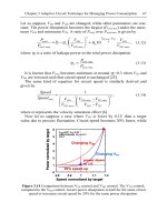
Fig. 4.21 MOSFET gate capacitance showing heavily doped polysilicon gate (dotted line)
and source/drain implanted n-doped polyside gate (continuous line) showing polysilicon
depletion effect. (From Chapman et al. [22])
degenerately doped, it can ncr longer be treated as an equipotential area.
This means that the capacitance describing the
MOS
capacitor can no
longer be given by
Eq.
(4.61)
and one needs to include the capacitance
Cpoly
due to the polysilicon gate. The resulting gate capacitance equation becomes
PO1
(4.78)
The result
of
the nondegenerate polysilicon is that the
LF
capacitance in
inversion
(Cg,inv)
is much smaller than in accumulation, and
Cg,inv
decreases
slightly with gate bias. However, at gate bias larger than a certain voltage
the
Cg,inv
recovers to
Cox
rather abruptly
[21]-[24].
This is shown in
Figure
4.21,
where high frequency C-V curve of an
MOS
capacitor (using
split-CV method13) is plotted for POCl, doped (dotted lines) and implanted
gate (continuous line). Note that in addition to the lowering of the gate
capacitance in inversion there is a slight shift in the flat band voltage
resulting in an increase in the threshold voltage
[24].
This anomalous C-V behavior has been explained assuming that there
exists a layer
of
partially activated dopants near the polysilicon/SiO,
interface
[23]
or by assuming that the polysilicon gate is non-degenerately
doped (concentration
-
1019cm-3)
[24].
When the gate bias is swept
positive
(for
the
As
implanted gate/SiO,/p-substrate), the p-substrate is
11 11
+-+
- -
-~
c,
Cpoly
cox
cs
l3
Split-CV method is discussed in section
9.9.1.