MOSFET MODELING FOR VLSI SIMULATION - Theory and Practice Episode 11 pdf
Bạn đang xem bản rút gọn của tài liệu. Xem và tải ngay bản đầy đủ của tài liệu tại đây (1.78 MB, 40 trang )
376
8
Modeling Hot-Carrier Effects
I
GATE
\
?O
T
"C
0
0-
*
A
5
U
B
S
1
RATE
i
fY
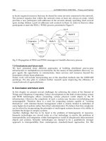
Fig.
8.5
Electron injection
in
gate oxide
showing
lucky electron model
electron arrives at location
D,
it will be swept toward the gate electrode
by the aiding field. Since the processes are statistically independent, the
resultant probability is the product of the probability for each individual
event, i.e.
[23]
(8.22)
where
2,
is the redirectional scattering mean free path. The factor
(dy/A,)
can be interpreted as the probability
of
redirection over
dy.
PI
is the prob-
ability for acquiring sufficient kinetic energy and normal momentum,
P,
is
the probability that a hot electron travels to the Si-SiO, interface without
suffering any inelastic collision, and
P,
is the probability to suffer no
collision in the oxide image-potential well. Thus, to calculate
I,,
we need
to calculate the three probabilities
P,,
P,
and
P,.
The essential processes
involved for modeling channel hot-electron injection into the gate oxide is
illustrated in Figure
8.6.
In order for the hot electron to surmount the Si-SO, potential barrier
Qb,
its kinetic energy must be greater than
qQb.
To acquire kinetic energy
qQb,
the hot electron will have to travel a distance
d
=
Qb/&
assuming the electric
field
6
along the channel to be constant. The probability of a channel
electron to travel a distance
d
or
more without suffering collision can be
written as
e-d/n,
where
A
is the scattering mean free path of the hot electron
[25].
Hence we can write
e-Qb/B*
as the probability that an electron will
acquire a kinetic energy greater than the potential barrier
Qb.
Now if the
electron
is
to
move into the oxide, its momentum must be redirected towards
the Si-SiO, interface by elastic scattering
so
as to have sufficiently large
momentum component perpendicular to the interface. It has been shown
that the probability
of
an electron acquiring the required kinetic energy
and retaining the appropriate momentum after redirection is
[23]
(8.23)
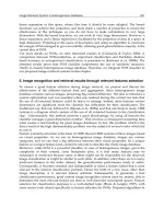
8.2
Gate Current Model
Pa
:
NO COLLISION
BEFORE
REACHING INTERFACE
371
Fig.
8.6
:
GAINS
ENOUGH
ENERGY
-
1
'
.
*-
>.:
prP3
:
NO COLLISION IN
FIELD REVERSAL REGION
BY
GATE
SILICON OXIDE METAL
T
L
Q,
E
ox
GATE
OXIDE METAL
L
E
ox
SILICON
Q,
The energy system for the
MOS
structure showing essential processes in
hot electron injection model. (After Tam et
al.
[23])
the channel
Since the potential barrier
Qb
is lowered by the image force effect, the net
barrier height is generally expressed as [22,23]
(8.24)
where
Qb0
=
3.2eV is the Si-SiO, interface barrier for the electrons,
€ox
is
the oxide field given by [cf.
Eq.
(6.195)]
a+,
=
mbo
-
2.59
x
10-4€;~
-
a,€;?
(8.25)
*ox
and
a,
is a constant whose value is obtained by fitting the experimental
data; Ning et al. [22] have assumed
a.
=
1
x
(cm), while Tam et al.
[23] find
a,
=
4
x
(cm) as a more appropriate value for their data.
The second term in
Eq.
(8.24)
represents the barrier lowering effect due to
the image field, while the third term accounts phenomenologically for the
finite probability of tunneling between the Si and SOz.
According to Tam et al. [23], the probability
P,
is given by
5.66
x
10-6€ox
P,
%
(1
+
80x/i.45
x
105)
+
2.5
x
lo-'
(8.26)
while the probability
P,
of
colision-free travel in the oxide-image potential
1
X
{
1
+
2
x
exp(
-
$€,,to,)}
378
8
Modeling Hot-Carrier Effects
well is given by
where
Lox
=
3.2 nm is the electron mean free path in the oxide. Note that
the product
of
P,
and
P,
is essentially only a function of the gate oxide
field
&ox,
therefore, it can be combined as
P,P,
=
P(&ox).
It is found that
P(&J
is a weak function of
&ox;
its value is maximum at the drain end
corresponding to the oxide field given by
Eq.
(8.25).
Since the probability
PI
depends exponentially on
&,
which in turn varies
exponentially with
y
[cf.
Eq.
(6.201)a], the integrant in
Eq.
(8.22) is a sharply
peaking function. Combining Eqs. (8.22)-(8.27) gives an approximate
expression for the gate current as
(8.28)
where
Ern
is the maximum channel field and
dbldx
z
bmm/lche
is assumed to
be constant over the length
lche
where
CHE
injection is significant. Since
value for
lche
is not known, it can be treated as a fitting parameter; however,
it can be replaced by
to,
without any loss
of
accuracy in the equation
above [23]. The
Eq.
(8.28) can now be integrated to give a closed form
expression for the gate current as
(8.29)
To
a first order above equation can be written as [6]
I,
z
c21dexp(
-
$)
(8.29a)
where C, is about 2
x
for
VgS
>
Vds.
Note that the only fitting param-
eters in Eq. (8.29) are
L
and
A,.
It was found that the gate current data
is insensitive to the value of
A,
and has been chosen to be 61.6nm based
on theoretical considerations [23]. The value of
A
which fits the data well
is found to be 9.2 nm. It is worth noting that
while the substrate current
I,
depends only on the channel electric jield
&rn,
the gate current
I,
is
a
function
of
both the channel jield
&m
and the normal oxide jield
&ox.
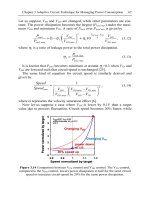
The gate current resulting from the channel hot-electrons in a nMOST
is shown in Figure
8.7
where circles are experimental data points while
continuous lines are calculated based on
Eq.
(8.29). Although the model is
not very accurate near the peak current, it nonetheless does model the
8.2
Gate Current Model
379
Fig.
8.7
Gate current
I,
in an nMOST as a function
of
V,,
at
V,,
=
10
V.
(After Tam
et
al.
[23])
general gate current behavior. The dependence of the gate current on the
channel length is apparent. Reduction of the channel length reduces
Vd,,,.
Therefore, for the same
vd,
the channel electric field
€,,,,
and hence
I,,
is
higher in shorter channel devices. The devices with thinner gate oxides
have higher gate current because of higher
€,,,
and
Figure
8.8
shows both gate and substrate current for an nMOST with
to,
=
200A
and
L
=
1.1
pm.
Note that peak gate current occurs at
V,,
z
Vd,
which is different from the peak of substrate current that occurs around
Vgs
z
Vds/2.
For
a
given
V,,,
the gate current
I,
increases with increas-
ing
V,,
due to increasing
€,,,
until
V,,
=
Vd,.
For
Vgs
>
Vd,,
MOSFET is
driven into the linear region of operation resulting in a reduction in
&,,,
and hence
I,.
The gate current shown in Figures
8.7
and
8.8
is due to
CHE
injection
into the gate oxide. However, it has been observed experimentally that gate
current in nMOST can also be generated by injection of hot holes into the
oxide (particularly thin gate oxide,
cox
<
150A) (see section
8.4)
[27]-[30]
These holes are produced by impact ionization of the channel hot-electrons
and are accelerated by the channel field. In order to evaluate this gate
current component, the hole generation due to impact ionization and lucky
electron probabilities for hole injection into the oxide must be modeled.
380
8
Modeling Hot-Carrier Effects
t,,=~OO
a
I-
'"0
2
L
6
8
10
12
GATE
VOLTAGE, V,,(V)
Fig.
8.8
Gate and substrate currents
I,
and
I,,
respectively, as a function
of
gate voltage
V,,
for different drain voltage
V,,
for a nMOST. (After Takeda et al.
[26])
I
I
-
p
MOST
L
=O.LVrn
t,,=105
A
-
-
0
-
0.0
2.5
GATE VOLTAGE,-Vg, (V)
Fig.
8.9
Gate and substrate currents
I,
and
I,,
respectively, as a function of gate voltage
V,,
for
different drain voltage
V,,
for
a
pMOST
8.2
Gate Current Model
38
1
The equivalent temperature model has also been used to model such hot-
hole injection
[28].
The gate current in a typical pMOST as a function of
V,,
and
V,,
is shown
in Figure
8.9; for the sake of comparison the substrate current is also shown.
Note that unlike in an nMOST, the peak of the gate current in a pMOST
occurs at much lower gate voltage, similar to that for the substrate current.
From the direction
of
the gate current measured at
low
and mid
V,,,
it is
found
that pMOST gate current is due to the avalanche hot-electrons (created
by
impact ionization ofholes) rather than the channel hot-holes
[24],
[31]-[33].
At higher
I
V,,l
one
expects the
pMOST
gate current to be composed
of
hot
holes, but measurable channel hot-hole injection current in pMOST has
not been reported. This is probably because of the large hole barrier height
and much shorter mean free path for holes in the oxide.
The electron gate
current in pMOST is often larger than the corresponding nMOSTgate current,
despite the fact that the number of available avalanche hot-electrons in
pMOST's is several orders of magnitude smaller than in nMOST's. This
happens because the direction of
€ox
is such that it aids electron injection
in pMOST while it opposes electron injection in nMOST for
V,,<<
Vd,.
For
V,,
>
Vd,,
is favorable but then its value is too small. Furthermore,
pMOST can take twice
as
large channel field as nMOST before breakdown.
The lucky electron model discussed earlier for the nMOST has also been
used to model the gate current in pMOST's
[24].
Since the source of hot
electrons resulting in the gate current in pMOST is from impact ionization
process which also produces substrate current
I,,
the pMOST gate current
Fig.
8.10
Gate
Circles are
current Ig as a function of Vgs at different Vas for pMOST. Circles are
experimental points
382
8
Modeling Hot-Carrier Effects
can be expressed as
and is obtained by replacing
I,
in Eq. (8.29) by
I,.
The pMOST gate current
calculated using Eq. (8.30) is shown in Figure 8.10 as continuous lines,
circules are measured data. The reasonable agreement between the model
and data validates Eq. (8.30).
8.3
Correlation
of
Gate and Substrate Current
Since the hot electrons responsible for the gate current and those responsible
for the substrate current are heated by the same field, it
is
expected that
the two currents will be correlated [34,35]. We can write Eq. (8.1 1) as
(8.31)
The above equation simply rewrites
Bi
=
QJl,
where
A
is the hot-electron
mean free path. In analogy with
Qb,Qi
can be interpreted as the energy
that an hot electron must have in order to create an electron-hole pair
through impact ionization, and exp(
-
is the probability that an
electron travel a distance
d
=
Qi/&,
to gain energy
qQi
or more without
1,
/Id
Fig.
8.11
Gate current
I,
against substrate current
I,
(both normalized to source current)
for constant values
of
V,,
-
V,,, and therefore of
&ox.
(After Tam et al.
[23])
8.4
Mechanism
of
MOSFET
Degradation
383
suffering collision. Eliminating
&m
from the exponential term in
Eq.
(8.29a)
and (8.31) we get
A= (?)
I
. (8.32)
Such a power law relationship is indeed observed as shown in Figure 8.11.
The slope of ln(I,/Id) versus ln(Ih/Id) gives the quantity
cDh/BiA.
Since
B,
and
J.
are independent of oxide field the slope can be used to find
@h
as a function of
€ox.
@b/B,1
Id
8.4
Mechanism
of
MOSFET Degradation
The hot-carrier effects result from large electric field in the channel (parti-
cularly near the drain end), which causes damage to the gate oxide (by charge
trapping in the oxide) and/or to the Si-SiO, interface (by generating interface
states). This leads to degradation of the n-channel MOSFET current drive
capability and affects parameters such as the threshold voltage
Vth,
the
linear region transconductance
gm,
the subthreshold slope
S,
and the satura-
tion region drive current
Idsat. Whether carrier (electron/hole) trapping or
interface generation is primarily responsible for the degradation is still
debated. But usually a net negative charge density is observed after long
time stressing as is evidenced by a threshold voltage
(VJ
increase in
nMOST's.
Figure 8.12 shows typical linear region
I,,
-
V,,
characteristics, before and
after stressing, which results in changes in
vh
and the peak transconductance
gm
(slope of the linear portion of the curve)
[6].
The device was a 100/2
nMOST with gate oxide thickness
to,
=
358
A;
and was stressed at
V,,
=
6
V,
V,,
=
7.5
V
for 90
minute^.^
Notice that the drain current reduces after
stressing and that the post-stress
I-V
characteristics are not symmetrical
with respect to the source/drain terminal because the damage is localized
at the drain end. This asymmetry is small in the linear region and is much
larger in the saturation region. This can be seen from Figure 8.13 which
shows typical
I,,
-
V,,
characteristics for a nMOST
(L
=
1.2 pm,
to,
=
200
A)
before and after stress
[24].
From this figure it is evident that
the drain
current reduction in saturation is much more severe in the reverse mode
compared
to
the forward mode.
Thus, device parameters change if the roles
Note that device stressing is done at accelerated voltages rather than at the normal
operating voltages. The underlying philosophy is that a phenomenon which occurs over a
short period under the action
of
accelerating stresses
is
indicative
of
a similar phenomenon
which will occur over a much longer period when the device is operating normally.
Accelerated stressing is necessary to study degradation in a reasonably short time.
384
8
Modeling Hot-Carrier Effects
11'
I
'I'
I'
I1
vss
(V)
Fig. 8.12 Degradation of nMOST linear region characteristics due to hot carrier injection
before and after stress. (After
Hu
et al.
[6])
"'"0.0 1.0
2.0
3.0
L-0
5.0
DRAIN
VOLTAGE,
V,,
(V)
Fig.
8.13
I,,
-
V,,
characteristics of a nMOST
(L
=
1.2pm and to,
=
200@ before and after
stress. Stress voltages
V,,
=
7.5
V
and
V,,
=
3
V.
Stress time
5
min. (After Ong et al. [24])
of source and drain are reversed after stressing, a condition that occurs in
transfer gates. An example of the degradation
of
a nMOST (L
=
0.77
pm)
on a log-log scale
is
shown in Figure
8.14
[40].
Here
Agm
=
gm(0)
-
gm(t)
is the difference between the device transconductance at times
0
and
t.
The
devices are stressed at
VgS
=
3
V
and
V,,
=
7
V
that corresponds
to
stress-
ing under peak substrate current condition.
The classical interpretation
of
the device degradation in n-channel devices
has been that only hot electrons can be injected into the gate oxide. How-
8.4 Mechanism
of
MOSFET Degradation
385
1
.o
n
MOST
h
0
v
E
E
zs,
,"
0.1
a
0.01
103
104
105
TIME
(sec)
Fig.
8.14
The degradation
of
n-channel
gm
at different temperatures. (After Yao et al. [40])
ever, recent studies show that hot hole injection is also possible [29]-[30].
These holes are produced by impact ionization and accelerated by the
channel field. This hole injection into the oxide is referred to as
hole current
and is usually very small, but it may have significant role in the degradation
of the device characteristics especially when
V,,
5
VdJ2 [41]. In fact, holes
need not even overcome the barrier but their field assisted tunneling is
adequate to cause serious damage to Si-SiO, interface. This is because
once holes are injected into the oxide, they are more likely to get trapped
than the electrons; the trapping efficiency of holes being close to 1, while
for
electrons it is less than
The hot-carrier effect involves the generation, injection and trapping of
carriers in the gate oxide.
Currier injection is a localized phenomenon;
it
takes place over only a fraction
of
the total length
of
the channel.
Four kinds
of hot-carrier generation/injection mechanism have been reported for
nMOST
[25],
[29], [37]. These are
(a)
Channel Hot Electrons
(CHE)
which are heated up in the channel
particularly near the drain end with the MOSFET operated at
V,,
=
V,,,
called the
lucky
electrons.
As
shown in Figure 8.15a, lucky electrons are
those flowing from source to drain gaining sufficient energy to surmount the
Si-SiO, barrier without suffering an energy loosing collision in the channel,
and thus move into the gate oxide resulting in the
so
called
gate current
I,.
This injection
of
hot electrons into the oxide is referred to as channel
hot electron
(CHE)
injection
[37].
The gate currents shown in Figures
8.5-
8.6
are due to
CHE
injection.
386
8
Modeling Hot-Carrier Effects
'b
(C)
'b
(d
1
Fig.
8.15
Four different injection mechanisms. (a) Channel Hot Electrons (CHE)
(b)
Drain
Avalanche Hot Carriers (DAHC), (c) Substrate Hot Electrons (SHE), and
(d)
Secondarily
Generated Hot Electron (SGHE)
(b)
Drain Avalanche Hot Carriers
(DAHC) which are due to the high electric
field near the drain region and promotes avalanche multiplication. The
electrons from the channel gain enough energy
so
that they produce electron-
hole pair by impact ionization which in turn produce further electron-hole
pairs resulting in an avalanche process. It is these avalanche hot electrons
and hot holes that are injected into the gate oxide, resulting in a gate
current with two peaks in the gate current versus gate voltage curves,
in addition to the CHE injection peak, as shown in Figure
8.16.
It is mostly
observed at the bias condition
V,,
>
V,,
>
V,,
in nMOST with
to,
<
150A.
Figure
8.15b
schematically illustrates the DAHC mechanism
[29].
The
DAHC
injection mechanism causes the most severe device degradation as
both holes and electrons are injected into the gate oxide.
(c)
Substrate Hot Electrons
(SHE),
which is due to the injection
of
thermally
generated or injected electrons from the substrate near the surface into the
8.4
Mechanism
of
MOSFET Degradation
387
10-9
,
1
V& -7v
10-10
~~
L
-0.52
-
9
10-11
tox
-1051
-
0,
n
MOST
z
W
u
3
0
10-14
+-
10-12
u:
10-13
Q
10-15
-~
c7
lg
(+)
k!
10-16
10-17
0.0
1.0
2.0
3.0
4.0
5.0
6.0
7.0
8.0
9.0
GATE VOLTAGE,
Vg,
(V)
Fig.
8.16
Measured gate current showing both electron and hole injection in n-channel gate
oxide
SiO,. It occurs when
Vd,
=
0,
Vgs
>
0
and large back bias
Vb,,
such as arises
in bootstrap circuits (Figure 8.15~). Electrons generated in the depletion
region,
or
diffusing from the bulk neutral region of the substrate, drift
towards the Si-SiO, interface. These electrons gain energy from the high
field in the surface depletion region, some
of
them having gained enough
energy to surmount the barrier.
SHE
injection, although less important
from a practical view point, due
to
the small number of thermally generated
electron-hole pairs, nevertheless has been thoroughly investigated in the
past
[37].
(d)
Secondarily Generated Hot electron
(SGHE),
which is that of secondary
minority carriers originated from secondary impact ionization of the sub-
strate current (Figure 8.15d). It occurs when substrate hole current, produced
by avalanche effect near the drain, generates further electron-hole pairs.
These secondary electrons are then injected into the oxide, as in the case
of
SHE
injection. This type of injection becomes particularly pronounced
for large back bias
V,b
and thin gate oxides
(tax
<
loo&. In fact, interface
generation due to hot holes and hot electrons has been reported for
0.25
pm
pMOST leading to a reduction in
gm
and
Id
with time
[38].
The hot-carrier effects in pMOST have been studied to a lesser extent
than nMOST. This .is because degradation in pMOST for
L
>
0.5pm
is considered a minor problem, due to the fact that the change in pMOST
characteristics after stress tends to saturate within an acceptable percentage.
One reason is higher barrier heights for holes (compared to electrons) at
the Si-SiO, interface.
A
further reason is the lower effectiveness of holes
388
8
Modeling Hot-Carrier Effects
I
IIIIIII
Fig.
8.1
7
I,,
-
V,,
characteristics of a pMOST
(L
=
1.2
pm
and
to,
=
200
A)
before and after
stress. Stress voltages
V,,
=
7.5
V
and
V,,
=
3
V.
Stress time
5
min.
(After
Ong et al.
1241)
in generating electron-hole pairs (i.e., smaller hole ionization coefficient).
This situation may change for deep submicron
(L
<
0.5
pm) devices with
pMOST becoming of concern.
Figure
8.17
shows typical
Id,
-
vd,
characteristics for pMOST before and
after stress
[24].
Note that while the drain current
Id
reduces after stress
in nMOST (see Figure
8.13),
it
increases in pMOST and
is
generally
considered to be unharmful. In fact, after stress pMOST
I
V,,l
decreases
(except at very high
I
V,J),
g,
increases, and subthreshold leakage current
increases (i.e., punchthrough voltage decreases)
[33].
This
is
in contrast with
increase in
v,,,
and decrease in
g,
in nMOST. It is generally believed that
after stressing of pMOST, avalanche hot electrons are trapped in the gate
oxide resulting in a negative charge near the drain. This leads to effective
shortening
of
the channel length and thus in an increase in the drain current.
Channel hot holes in pMOST do not play any significant role. However,
in nMOST both channel hot electrons and avalanche hot holes are important
in hot carrier induced degradation.
8.5
Measure
of
Degradation-Device Lifetime
It is common to characterize the device degradation
by
measuring shifts
in the threshold voltage
AV,,,
change in the transconductance degradation
Ag,/g,,
or
change in the drain current
Ald/ld
before and after the device
is stressed. It has been observed that
V,,
shift,
or
g,
degradation, can well
be expressed as
[7],
[39]
Ald/ld
(Or
Av,,,
Or
Agm/g,)
=
A.t"
(8.33)
8.5
Measure
of
Degradation-Device Lifetime
389
where
t
is the stress time. Equation (8.33) is valid for almost all
MOS
devices, in particular, at short stress time; at long stress time
V,h
shift and/or
g,
degradation rather saturates. The slope
n
in a log-log plot of
t
versus
AVth
is strongly dependent on
V,,
but has a week dependence on
V,,.
This
suggests that
n
changes according to hot-carrier injection mechanism. In
case of DAHC mechanism
n
FZ
0.5-0.7 for devices with
to,
=
68-200
8,
and
L
=
0.35-2pm. On the other hand
A,
which represents the magnitude of
degradation, is strongly dependent on
Vd,
[A
K
exp(
-
l/vds)]. Figure 8.18a
is
a plot of
Ag,
versus stress time on a log-log scale for nMOST
(L
=
0.48 pm
and
to,
=
105
A).
All devices are stressed under peak substrate current
conditions. For pMOST
n
FZ
0.15-0.25 [40], which is much smaller than
for nMOST, showing smaller degradation for pMOST. The
g,
degradation
in pMOST is shown in Figure 8.18b. Note that pMOST do not obey the
power law equation(8.33) but rather has been observed to obey a log-
arithmic time dependence [43-441. This has been interpreted as being due
either to a reduction in the lateral electric field with stressing time [43],
or due to a shifting point of carrier injection.
Figure 8.19 shows the relationship between
g,
degradation, generated
surface states
Nit
and substrate current
I,
in an nMOST with
L
=
0.8
pm
and
to,
=
200A. The stress conditions were
V,,
=
6.6 V,
V,,
=
3 V and stress
time
=
lo4
sec.
A
remarkable correlation between the peak of the substrate
current
I,,
g,
degradation and
Nit
generation leads one to conclude that the
device degradation can be monitored using the substrate current. In contrast,
in this bias range the gate current
I,
increases exponentially suggesting
that degradation may not be correlated to the gate current (for nMOST).
If we define lifetime
z
as the stress time at which the change
A
in
T/rh,
g,
or
Idsa,
reaches a certain failure criterion such that
AVth
=
10
mV, Ag,/g,
=
10%
or
AId/Id
=
lo%,
then under conditions of DC stress we find [39]
z
=
c.z,m
(8.34)
where
C
is a process dependent constant, while
m
FZ
3 is constant for a large
number of NMOS/CMOS technologies with different
to,,
S/D
structure
and channel length [6,7].
To
determine
z
from
Eq.
(8.34),
devices are gene-
rally stressed at various values
of
V,,
with
V,,
adjusted for maximum substrate
current (which is found to correspond to maximum degradation).
It should be pointed out that Eq. (8.34) is valid
so
long as
V,,
is not varied
too extensively as degradation and substrate current
do
not correlate
perfectly; i.e., the peak of degradation does not exactly coincide with the
peak
of
I,
[41]. In such situations it is more appropriate to use the follow-
ing expression for lifetime due to
DC
stress conditions [7], [41]
=
cl(zb/zd)-m/ld
(8.35)
where
m
varies from 3-5. The plot of
zI,/W
versus
Ib/Id
on a log-log scale
will be a straight line, the slope and intercept of which gives the degradation
390
8
Modeling Hot-Carrier Effects
L
-
0.65
0.1
0
h
c
v
E
0,
E
\
a"
0.01
1
10' 102 103 104
(a)
TIME
(sec.)
10-3
J
0.0
10' 102 103 104 105
TIME
(sec.)
(b)
Fig.
8.18
Device degradation as a function of time for (a) n-channel device and
(b)
p-channel
device
8.5
Measure of Degradation-Device Lifetime
39
1
nMOST
2L68
STRESS GATE VOLTAGE, VgS(V)
Fig.
8.19
Correlation between transconductance degradation
gm,
substrate current
I,
and
density of interface states
Nit,
exhibiting similar variation with
Vgs.
L
=
0.8
pm,
to,
=
200
A,
V,,
=
6.6V
and V,,
=
3
V.
(After Takeda et al.
[36])
parameters
rn
and
C,.
Note that the drain current
Id
is per unit width
W
Previous studies on near micron devices showed that nMOST degradation
is technology dependent and is relatively independent of the channel length
for stress at the same
I,
[6].
However, recent studies have shown that the
effect of device degradation on device performance is more prominent in
short-channel submicron regime nMOST
[lo].
This is because device
degradation is a localized phenomena, therefore, it is expected that hot-
carrier created damage near the drain end will be independent of the channel
length for the same amount
of
stress
(1;.
t
=
const). In other words, the ratio
of
the damaged interface area to the total channel area increases as the
channel length decreases, and thus device lifetime decreases because the
relative amount
of
degradation increases. Equations
(8.34)
and
(8.35)
have
been slightly modified to take account for the channel length dependence
on device degradation
[42].
Thus, Eq.
(8.34)
is modified as
z
=
C,L"2.
r,m
(8.36)
where
n2
=
2-3.
Equation
(8.35)
can be modified in a similar way to take
into account the dependence
of
z
on
L.
(Id/
w)*
392
8
Modeling
Hot-Carrier
Effects
For n-channel MOSFETs,
I,,
or
(Ib/Id)
is
a
well accepted monitor for hot-
carrier induced degradation. However, for p-channel MOSFETs both
1,
[45]
and
I,
[46] have been used as monitors, although degradation follows
I,
better than
1,
[43].
It has been suggested that for electron trapping
damage in pMOST, where
gm
and
I,
increase,
I,
should be used; whereas
for interface state generation in very short channel pMOST
(L
<
0.5
pm),
where
gm
and
Id
decrease,
1,
should be used as the monitor for
z
measure-
ment
[38].
If
I,
is taken as the monitor, then pMOST lifetime can
be
expressed as
z
=
C,Z,-"
@MOST)
(8.37)
where constant
m
=
1.5
[24]
as against
3
for nMOST.
Dynamic
Stressing.
Although MOSFETs in circuits are subjected to transient
gate and drain voltage conditions, their hot carrier reliability has often
been evaluated based upon the model for static or DC stress, as given by
Eqs.
(8.34)-(8.35).
In many of these studies AC stress life time
zAC
has
been compared to the lifetime predicted by quasi-static application
of
Eq.
(8.35)
for nMOST
[8], [41]
and Eq.
(8.37)
for pMOST
[47].
Thus, for
example,
zAC
for nMOST is given by
(8.38)
where
T
is the full cycle time,
I,
and
Id
are the currents at time
t(
I
T).
The degradation parameters
rn
and
H
are in general gate and drain bias
dependent
[8].
However, it has been observed that stress undCr AC,
or
dynamic conditions, can be significantly worse than might be expected from
the quasi-static sum of DC stresses given by Eq.
(8.38).
Recently much
attention has been focused on this enhanced AC stress effect
[48]-[55].
Due
to
severe degradation in nMOST, dynamic
or
AC stress analysis has
been studied mainly in nMOST. What follows is for n-channel devices.
Early reports showed that enhanced AC degradation was the result of
enhanced substrate currents during falling gate voltage edges and shorter
transition times
[48]-[52].
The phenomenological link between substrate
current and hot-carrier degradation [see Eq.
(8.34)]
then explained the
enhanced AC degradation. However, later reports failed to confirm any
substrate current enhancement, at least for rise/fall times as low as
3ns,
and the apparent increase in the substrate current was linked to the measure-
ment difficulties
[53]-[55].
It was also pointed out that the discrepancy
between DC and AC stress could be due to the fact that Eqs.
(8.34)
or
(8.35)
do not adequately model all aspect
of
hot-carrier damage. Indeed in
the absence of any 'transient effect', this is likely the case as has been
pointed out by Mistry and coworkers
[55]-[58].
They have shown that
8.5
Measure
of
Degradation-Device Lifetime
393
enhanced AC degradation is due to the presence of three different damage
modes, rather than the one mode which traditionally has been associated
with peak substrate current region, and is thought to be due to interface
state generation. The three modes of degradations are
(1)
electron trap
creation and interface state generation by hot holes
(Nox,J
taking place
at
low gate voltages,
(2)
electron trapping by hot electrons
(iVoX,J
occurring
at
high
gate voltages,
and (3) interface state creation
(NJ
which occurs at
intermediate gate voltages,
around the peak of the substrate current.
All
the three types of damage contribute to device degradation during AC
stress. The lifetime due to these damages are empirically modeled
as
[58]
(8.39a)
(8.39 b)
(8.39~)
where
A,, A,, A,
and
m,, m2,m3
are empirical constants. Note that Eq. (8.39~)
is valid only for
Vgs
such that the gate current is negative (i.e., consists
primarily of electrons). As
an
approximation, it is valid for
Vgs
>
Vds/2.
In order to estimate AC stress lifetimes, we must first calculate the quasi-
static contributions for the three damage modes by integrating
Eqs.
(8.39)
over the time period
T
of
the AC stress waveform. For example, the value
of
z~~~,~
is calculated as
(8.40)
where quasi-static values are used for all currents. The values of
zN,,
and
zN,,,,
are similarly calculated.
In
this integration procedure,
l/z
is treated
as
a
damage function which is integrated over the time period of the AC stress
waveform for each of the three damage modes. The following Matthiessen-
like rule is then used to calculate the lifetime taking all three damage modes
into account
[SS]
(8.41)
The damage functions for the three damage modes are added together in
order to calculate the total damage. Figure
8.20a
shows the measured AC
stress lifetime (dotted lines) compared to that calculated (continuous lines)
using the above model for a stress waveform resembling inverter-like AC
stress. Figure 8.20b shows the damage contributions of the three damage
modes.
Instead of using three damage mode equations
as
discussed above, Hu and
coworkers have used
Eq.
(8.38) with
H
and
m
as bias dependent param-
eters to account for higher degradation under dynamic stressing
[S],
C.591-
[61].
Phenomenologically bias dependent
of
H
and
m
accounts for different
damage mechanism under different bias conditions.
'IZAC
=
l/zNss
+
'/'Nox,h
+
l/zNox,e'
394
8
Modeling Hot-Carrier Effects
v,,
(V)
(b)
Fig.
8.20
(a) Measured
(0)
and calculated
(0)
AC stress lifetimes
for
inverter-like stress
versus
V,,
=
4.3
V.
(b) Calculated contributions
of
the three damage modes to the AC lifetimes
for
Noxh(0),
N,,(V),
and
Noxe(A).
(After Mistry et al.
[SS])
8.6
Impact
of
Degradation on Circuit Performance
In the previous sections we have discussed models for MOSFET substrate
and gate currents that are related to the device lifetime models based on
device-level degradation parameters
AV,,,
Agm/gF,
etc. By combining these
models in a pre- and post-processor configuration to a circuit simulator
such as SPICE, one can calculate lifetime of each device in a circuit under
operating conditions. Thus, the device lifetime can be estimated in a circuit
environment. This is the approach used in most
of
the circuit reliability
simulators to assess the circuit level performance as a function of hot-carrier
stress
[8], [lg], [60]-[64].
One such simulator called
SCALE
(Substrate
Current And Lifetime Evaluator) was developed at the University of
California, Berkeley
[8].
In a pre-processor configuration
SCALE
calls
SPICE to calculate the transient voltage waveforms at the drain, gate,
8.6
Impact
of
Degradation on Circuit Performance
395
source and substrate of the user selected devices. The post-processor then
calculates the transient substrate current based on transient terminal
voltages. The substrate current in turn is used to calculate device lifetime.
In the Berkeley version of SCALE, drain currents are obtained from the
BSIM model (Level
=
4) and the device lifetime is calculated using Eq. (8.38).
However, one can implement substrate current and device lifetime models
in SCALE that are more appropriate for a particular technology [lS].
Although using SCALE one can flag devices that have high substrate
current and hence low lifetime, the relationship between individual device
degradation and circuit degradation as a whole remains ambiguous. This
is because not all transistors affect circuit behavior in the same way
[60]-[64]. For example, in a circuit one transistor
MI
may degrade much
more severely than other transistor
M,,
but circuit performance may
depend more on
M,
than
MI.
The sensitivity of this dependence may also
change depending on what characteristic of the circuit is studied. Simple
device failure criterion such as setting device lifetime at
Al!s/Ids
=
10% may
often be misleading when applied generally. It is, therefore, imperative that a
simulator be able
(1)
to predict the degradation of each transistor while
operating in a circuit environment for user-definable length of time and,
(2) to directly simulate the entire circuit using degraded device parameters
obtained from the information in step
1.
The simulator CAS (Circuit Aging
Simulator)' simulates circuits undergoing dynamic degradation for a user
defined length of time [59]-[60]. CAS incorporates the structure and model
of SCALE; in fact SCALE is a subset of CAS.
A
new parameter
Age,
is
introduced to quantify the amount
of
degradation each device experiences
during circuit operation and is defined as
(8.42)
for nMOST, while for pMOST the ratio
lr/I:-'
is
replaced by
1;
or
sum
of the two with weighting factors [61]. In Eq. (8.42)
H
and
m
are gate and
drain bias dependent degradation parameters,
t
is the circuit operating
time, and
W
is device width. During circuit simulation, the
Age
is calculated
for each device
at
each time-step, then integrated
to
obtain the total Age
for the SPICE analysis. After the
Age
of each transistor in the circuit is
calculated by this quasi-static method, the aged process files corresponding
to the individual transistors is then used to simulate the actual circuit
degradation for a user specified period of time.
Both SCALE and CAS are based on the assumptions that (1) SPICE
analysis must be transient analysis since aging is based on time; and (2)
CAS
is
now
replaced by BErkeley Reliability
Tool
called BERT [60].
396
8
Modeling
Hot-Carrier
Effects
circuit behavior is assumed to be periodic with the period equal to the
length of the
SPICE
analysis.
8.7
Temperature Dependence
of
Device Degradation
The device degradation depends upon gate and substrate current, which
in turn depends upon drain current. Since
I,
is temperature dependent (cf.
section 6.9), it is expected that
I,
and
1,
will be temperature dependent.
Experimentally
it
is found that the device degradation increases as tempera-
ture is lowered (see Figure 8.14) and hence device life-time becomes shorter
at lower temperature (see Figure 8.20)
[65]-1681.
Intuitively this could be
understood as follows. Lowering the temperature results in an increased
injection of hot electrons into the gate oxide and hence gate current increases
[69]. Similarly lowering the temperature increases the optical-phonon mean
free path
/z
and thus the energy
(A&,,,)
acquired by hot carriers by the field,
thereby increasing substrate current [cf. Eq. (8.3
l)].
The temperature coefficient of the gate current (d(ln(Ig/Id))/dT) is higher
(-
O.O256/"C) compared to the substrate current
(-
O.O132/"C) [23]. From
Eq. (8.32) one expects the slopes of Ig/Id and
Ib/ld
versus temperature to
differ by a factor of
Qb/(BiA)
%
2.1. Increased device degradation at lower
temperature can also be understood from the fact that lowering the tem-
perature increases rate of hot-electron trapping. Higher density of traps
and/or oxide charge will result in higher mobility degradation and threshold
voltage shift.
Modeling Temperature Dependence
of
Substrate Current. Experimentally
it is observed that
I,
exhibits higher temperature dependence compared
to
1,.
Figure 8.21 shows
a
plot of
I,
versus
VgS
for an n-channel device
(L
=
0.78 pm) at three temperatures 0,25 and 100 "C.
As
can be seen from
this figure
I,
decreases as temperature increases, consistent with the
I,
temperature dependence. The normalized temperature coefficient of
I,
in
the temperature range 0-120°C is approximately given by
[lS]
(8.43)
while the normalized temperature coefficient of
I,,
in saturation, for the
same device as shown in Figure (8.21) is
1
ar,
%3
x
lop3
(/"C)
I,
aT
(8.44)
which is very close to the temperature coefficient of
1,.
This implies that
the rest of the parameters in Eq. (8.12) account for the difference.
8.7
Temperature Dependence of Device Degradation
397
1.12
I
I
I
I
I-
Z
w
II
rr
0.56
0
0.6
2.3
4
GATE VOLTAGE,
Vg,
(V)
Fig.
8.21
Substrate current
I,
as a function of
VgS
at
V,,
=4.6V,
Vsb=OV
for a typical
nMOST at three temperatures
0,25
and
100
C
It has been shown
[18],
[66]
that
Eq.
(8.12) agrees with the experimental
data in the temperature range
400 K-77 K
provided temperature dependence
of
(1)
the drain current,
I,,
(2)
the ionization coefficients
A,
and
Bi,
and
(3)
the effective ionization length,
1
are taken into account. It has been observed
that the ionization coefficient
A,
is almost independent of temperature and
it is the temperature dependence of
B,
which accounts for the temperature
dependence of the ionization rate
a,,
[18].
The following linear relation of
the coefficient
B,
with temperature is assumed
=
BioC1+
PB,('-
(8.45)
where
Bio
represent the values
of
the ionization constants
Bi
at the reference
temperature
T
=
To
(say,
300
K), and
ljB,
is
the temperature coefficients of
Bi
whose value is found to be
[18]
(8.46)
1
dB.
B'-
B,
dT
=
-
2
=
9.28
x
lop4 Kpl (electrons).
This value is consistent with that reported by Grant
[70].
The following linear relation for the temperature dependence
of
1
is generally
used
(8.47)
U)
=
wIo)C1
+
MT-
To)]
398
8
Modeling Hot-Carrier Effects
where the parameter,
pi,
is
the temperature coefficient
of
1
and
is
obtained
by curve fitting the experimental
I,
data to
Eq.
(8.12)
with
Bi
and
1
given
by
Eqs.
(8.45)
and
(8.47),
respectively. This approach
is
adequate to model
the temperature dependence
of
Isub,
which has been tested in the temperature
range
273
K-400
K,
as shown by the continuous line in Figure
8.21.
References
[
11
R.
R.
Troutman, ‘Low-level avalanche multiplication in IGFETs’, IEEE Trans.
Electron Devices, ED-23, pp. 419-425 (1976).
[2] Y. A. El-Mansy and D. M. Caughey, ‘Modeling weak avalanche multiplication
currents in IGFETS and
SOS
transistors
for
CAD’, IEEE IEDM-75,
Dig. Tech. Papers,
[3]
S.
Selberherr,
Analysis and Simulation
of
Semiconductor Devices,
Springer-Verlag, Wien,
New-York, 1984.
[4]
J.
W.
Slothoom,
G.
Streutker,
G.
J.
T. Davids, and
P.
B.
Hartog, ‘Surface impact
ionization in silicon devices’, IEEE IEDM-87,
Dig. Tech. Papers,
pp. 494-497 (1987).
[5] A. Erdelyi,
Asymptotic Expansions,
Dover Publications Inc, New York, 1956.
[6] C. Hu,
S.
C. Tam, F.
C.
Hsu,
P.
K.
KO,
T.
Y. Chan, and
K.
W. Terrill, ‘Hot-electron
induced MOSFET degradation-model, monitor, and improvement’, IEEE Trans.
Electron Devices, ED-32, pp. 375-385 (1985).
171 C. Hu, ‘Hot carrier effects’, in
Advanced
MOS
Device Physics
(N.
G.
Einspruch and
G. Gildenblat, eds.), VLSI Electronics Vol. 18, pp. 119-139, Academic Press Inc.,
New York, 1989.
[S] M. M.
Kuo,
K.
Seki,
P.
M. Lee,
J.
Y. Choi,
P.
K.
KO,
and C. Hu, ‘Simulation
of
MOSFET lifetime under AC hot-electron stress’, IEEE Trans. Electron Devices,
ED-35,
[9] T C. Ong,
P.
K. KO,
and C.
Hu,
‘Modeling
of
substrate current in p-MOSFET’s’,
IEEE Trans. Electron Device Lett., EDL-8, pp. 413-416 (1987).
[lo] J. Chung, M. C. Jeng,
G.
May,
P.
K.
KO,
and
C.
Hu, ‘Hot-electron currents in deep-
submicrometer MOSFETs’, IEEE IEDM-88,
Dig.
Tech. Papers,
pp. 200-203 (1988).
[Ill Y. Tang,
D.
M. Kim, Y H. Lee, and
B.
Sahi, ‘Unified characterization
of
two-region
gate bias stress in submicrometer p-channel MOSFETs’, IEEE Electron Device Lett.,
[12]
J.
Faricelli and
G.
Gildenhlat, ‘Numerical verification
of
substrate current model in
silicon IGFET’s’, Solid-state Electron.,
30,
pp. 655-660 (1987).
[13] J. Mar,
S. S.
Li, and
S.
Y.
Yu,
‘Substrate current modeling
for
circuit simulation’,
IEEE Trans. Computer-Aided Design, CAD-1, pp. 183-186 (1982).
[
141 Y.
W.
Sing and
B.
Sudlow, ‘Modeling and VLSI design constraints
of
substrate current’,
IEEE IEDM-80,
Dig. Tech. Papers,
pp. 732-735 (1980).
[l5] T. Sakurai,
K.
Nogami,
M.
Kakumu, and T. Iizuka, ‘Hot-carrier generation in
sub-
micrometer VLSI environment’, IEEE
J.
Solid-state Circuits, SC-22, pp. 256-259
(1987).
[16] T. Y. Chan,
P.
K.
KO,
and
C.
Hu,
‘A
simple method to characterize substrate current
in MOSFETs’, IEEE Trans. Electron Device Lett., EDL-5, pp. 505-507 (1984).
[17]
T.
Y. Chan,
P.
K.
KO, and C. Hu, ‘Dependence
of
channel electric field in device
scaling’, IEEE Electron Device Lett., EDL-6, pp. 551-553 (1985).
[IS]
N.
D.
Arora and M. Sharma, ‘MOSFET substrate current model
for
circuit simulation’,
IEEE Trans. Electron Devices, ED-38, pp. 1392-1398 (1991).
[I91
Y. Tang, D. M. Kim, ‘Modeling
of
on-state MOSFET operation and derivation
of
maximum channel field’, IEEE Trans. Electron Devices, ED-38, pp. 2472-2480 (1991).
pp. 31-34 (1975).
pp. 1004-1010 (1988).
EDL-11, pp. 203-205 (1990).
References 399
W. Shockley, ‘Problems related to pn junction in silicon’, Solid-State Electron.,
2,
J.
F.
Verwey,
R.
P. Kramer, and
B.
J.
de Maagt, ‘Mean free path
of
hot electrons at
the surface
of
boron doped silicon’,
J.
Appl. Phys., 46, pp. 2612-2619 (1975).
T. H. Ning, C. M. Osburn, and H. N. Yu, ‘Emission probability
of
hot electrons from
silicon into silicon dioxide’,
J.
Appl. Phys., 48, pp. 286-293 (1977).
S.
Tam, P. K.
KO,
and
C.
Hu, ‘Lucky-electron model
of
channel hot electron injection
in MOSFETs’, IEEE Trans. Electron Devices, ED-31, pp. 1116-1125 (1984).
T C. Ong, P.
K.
KO, and
C.
Hu, ‘Hot-carrier current modeling and device degradation
in surface-channel p-MOSFETs’, IEEE Trans. Electron Devices, ED-37, pp. 1658-1666
(1990).
P. E. Cottrell, R.
R.
Troutman, and T. H. Ning, ‘Hot-electron emission in n-channel
IGFETs’, IEEE Trans. Electron Devices, ED-26, pp. 520-533 (1979).
E. Takeda,
H.
Kume, T. Toyabe, and
S.
Asai, ‘Submicrometer MOSFET structure
for
minimizing hot-carrier generation’, IEEE Trans. Electron Devices, ED-29, pp. 61 1-
618 (1982).
K.
R.
Hofmann, C. Werner, W. Weber, and
G.
Dorda, ‘Hot-electron and hole-emission
effects in short n-channel MOSFETs’, IEEE Trans. Electron Devices, ED-32, pp. 691-699
(1985).
M. Miura-Mattausch, A. V. Schweri,
W.
Weber, C. Werner, and
G.
Dorda, ‘Gate
currents in thin oxide MOSFETs’, IEE Proceedings, 134, Pt.
I,
pp. 11 1-1 15 (1987).
E. Takeda, ‘Hot-carrier effects in submicrometer MOS VLSI’, IEE Proceedings, 131,
N.
S.
Saks, P. L. Heremans,
L.
Van den Hove,
H.
E. Maes,
R.
F.
De Keersmaecker,
and
G.
J.
Declerck, ‘Observation
of
hot-hole injection in NMOS transistors using a
modified floating gate technique’, IEEE Trans. Electron Devices, ED-33, pp. 1529-
1534 (1986).
K. K. Ng and
G.
W. Taylor, ‘Effects
of
hot-carrier trapping in
n-
and p-channel
MOSFETs’, IEEE Trans. Electron Devices, ED-30, pp. 871-876 (1983).
T. Tsuchiya and
J.
Frey, ‘Relationship between hot-electrons/holes and degradation
for p- and n-channel MOSFETS’, IEEE Electron Device Lett., EDL-6, pp. 8-1
1
(1985).
M. Koyanagi, A. G. Lewis,
J.
Zhu,
R.
A. Martin, T. Y. Huang, and
J.
Y. Chen, ‘Hot
electron induced punchthrough (HEIP) effect in submicron PMOSFETs’, IEEE Trans.
Electron Devices, ED-34, pp. 839-844 (1987).
S.
Tam, P.
K.
KO,
C. Hu, and
R.
S.
Muller, ‘Correlation between substrate and gate
currents in MOSFETs’, IEEE Trans. Electron Devices, ED-29, pp. 1740-1744
(1982)
S.
Tanaka and
S.
Watanabe, ‘A model for the relation between substrate and gate
currents in n-channel MOSFETs’, IEEE Trans. Electron Devices, ED-30, pp. 668-675
(1983).
E. Takeda, A. Shimizu, and T. Hagiwara, ‘Role of hot-hole injection in hot-carrier
effects and the small degraded channel region in MOSFETs’, IEEE Electron Device
Lett., EDL-4, pp. 329-331 (1983).
T.
H.
Ning, P.
W.
Cook,
R.
H.
Dennard,
C.
M. Osburn,
S.
E. Schuster, and
H N.
Yu,
‘1
pm MOSFET VLSI technology: Part IV: Hot-electron design constraints, IEEE
Trans. Electron Devices, ED-26, pp. 346-353 (1979).
T. Tsuchiya, Y. Okazaki, M. Miyaka, and T. Kobayashi, ‘New hot-carrier degradation
mode in lifetime prediction method in quarter-micrometer PMOSFET’, IEEE Trans.
Electron Devices, ED-39, pp. 404-408 (1992).
E. Takeda and N. Suzuki, ‘An empirical model
for
device degradation due to hot-carrier
injection’, IEEE Electron Device Lett., EDL-4, pp.
11
1-1
13
(1983).
C.
Yao,
J.
Tzou, and R. Cheung, ‘Temperature dependence
of
CMOS device reliability’,
IEEE IRPS-86,
Tech.
Dig.,
pp. 175-182 (1986).
pp. 35-67 (1961).
Pt.
I,
pp. 153-164 (1984).
[20]
[21]
[22]
[23]
[24]
[25]
[26]
[27]
[28]
[29]
[30]
[31]
[32]
[33]
[34]
[35]
[36]
[37]
[38]
[39]
[40]
400 8 Modeling Hot-Carrier Effects
[41] W. Weber, C. Werner, and A. Schwerin, ‘Lifetimes and substrate currents in static and
dynamic hot carrier degradation’, IEE-IEDM86,
Tech.
Dig.,
pp. 390-393 (1986).
[42]
K.
R.
Mistry and B.
S.
Doyle, ‘An empirical model for the
L,,,
dependence
of
hot-carrier
lifetimes of n-channel MOSFETs’, Electron Device Letters, EDL-10, pp. 500-502
(1989).
[43] B.
S.
Doyle and
K.
R. Mistry,
‘A
lifetime prediction method for hot-carrier degradation
in surface-channel p-MOS devices’, IEEE Trans. Electron Devices, ED-37, pp. 1301-
1307 (1990).
[44] M. Brox, E. Wohlrab, and W. Weber, ‘A physical lifetime prediction method for
hot-carrier-stressed p-MOS transistors’, IEEE IEDM-91,
Tech.
Dig.,
pp. 525-528
(1988).
[45] W. Weber and F. Lau, ‘Hot-carrier drifts in submicrometer p-channel MOSFETs’,
IEEE Electron Device Lett., EDL-8, pp. 208-211 (1987).
[46] M.
P.
Brassington, M. W. Poulter, and
M.
El-Diwanay, ‘Suppression of hot-carrier
effects in sub&rometer surface-channel PMOSFETs’, IEEE Trans. Electron Devices,
T C. Ong,
K.
Seki, P.
K. KO,
and C. Hu, ‘Hot-carrier-induced degradation in
p-
MOSFET’s under AC stress’, IEEE Trans. Electron Device Lett., EDL-9, pp.
21
1-213
(1988).
K.
L. Chen,
S.
Saller, and
R.
Shah, ‘The case
of
AC stress in the hot carrier effect’,
IEEE Trans. Electron Devices, ED-33, pp. 424-426 (1986).
J.
Y.
Choi,
P.
K.
KO,
and C. Hu, ‘Hot-carrier-induced MOSFET degradation under
AC stress’, IEEE Electron Device Letters, EDL-8, pp. 333-335 (1987).
H.
Wang, M. Davis, and R. Lahri, ‘Transient substrate current effects on n-channel
MOSFET device lifetime’, IEEE IEDM-88,
Tech.
Dig.,
pp. 216-219 (1988).
H. Wang,
S.
Bibyk, M. Davis,
H.
De, and
Y.
Nissan-Cohen, ‘Transient hot-electron
effect on n-channel device degradation’, IEEE IEDM-89,
Tech.
Dig.,
pp. 79-83 (1989).
R. Bellens,
P.
Heremans, G. Groenseneken, and H. E. Maes, ‘Analysis of the mechanisms
for the enhanced degradation during AC hot carrier stress of MOSFETs’, IEEE
IEDM-88,
Tech.
Dig.,
pp. 212-215 (1988).
W. Hansch and W. Weber, ‘The effect
of
transients on hot carriers’, IEEE Electron
Device Letters, EDL-10, pp. 252-255 (1989).
R.
Bellens, P. Heremans,
G.
Groeseneken, H. E. Maes, and W. Weber, ‘The influence
of measurement setup on enhanced AC hot carrier degradation of MOSFETs’, IEEE
Trans. Electron Devices, ED-37, pp. 310-313 (1990).
K.
R.
Mistrv and B.
S.
Dovle. ‘The role of electron traD creation in enhanced hot-carrier
ED-35, p. 1149 (1988).
degradation during AC stress’, IEEE Electron Device Letters, EDL-11, pp. 267-269
(1990).
B.
S.
Doyle, M. Bourecerie, C. Bergonzoni, R. Benecchi, A. Bravis,
K.
R.
Mistry, and
A. Boudou, ‘The generation and characterization of electron and hole traps created
by hole injection during low gate voltage hot-carrier stressing of n-MOS transistors’,
IEEE Trans. Electron Devices, ED-37, pp. 1869-1876 (1990).
K.
R. Mistry and B.
S.
Doyle,
‘A
model for AC hot-carrier degradation in n-channel
MOSFETs’, Electron Device Letters, EDL-12, pp. 492-494 (1991).
K.
R. Mistry, B.
S.
Doyle, A. Philipossian, and D. B. Jackson, ‘AC hot carrier lifetimes
in oxide and
ROXNOX
n-channel MOSFETs’, IEEE-IEDM91,
Tech.
Dig.,
pp. 727-730
(1991).
P.
M.
Lee,
M.
M.
Kuo,
K.
Seki, P.
K.
KO,
and C.
Hu,
‘Circuit aging simulator (CAS)’,
IEEE-IEDM88,
Tech.
Dig.,
pp. 134-138 (1988).
P.
M. Lee, M. M.
Kuo,
P.
K.
KO,
and
C.
Hu, ‘BERT-A circuit aging simulator’,
Memo.
No.
UCB/ERL M90/2, Electronics Research Lab., University of California,
Berkeley, 1990.
[47]
[48]
[49]
[50]
[51]
[52]
[53]
[54]
[55]
[56]
[57]
[58]
[59]
[60]