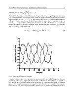
Introduction to Electronics - Part 2 docx
Bạn đang xem bản rút gọn của tài liệu. Xem và tải ngay bản đầy đủ của tài liệu tại đây (146.82 KB, 20 trang )
Introduction to Electronics
11
Power Supplies, Power Conservation, and Efficiency
+
+
-
-
v
s
v
i
A
voc
v
i
v
o
++
R
S
R
L
R
i
R
o
i
i
i
o
Source Amplifier Load
V
AA
-V
BB
I
A
I
B
V
AA
V
BB
+
+
-
-
Fig. 23. Our voltage amplifier model showing power supply and ground connections.
PVIVI
SAAABBB
=+
(13)
PPPP
Si oD
+=+
(14)
Power Supplies, Power Conservation, and Efficiency
The
signal power
delivered to the load
is converted from the
dc
power provided by the power supplies
.
DC Input Power
This is sometimes noted as
P
IN
.
Use care not to confuse this with
the signal input power
P
i
.
Conservation of Power
Signal power is delivered to the load
P
o
⇒
Power is dissipated within the amplifier as heat
P
D
⇒
The total input power must equal the total output power:
Virtually always
P
i
<<
P
S
and is neglected.
Introduction to Electronics
12
Power Supplies, Power Conservation, and Efficiency
+
+
-
-
v
s
v
i
A
voc
v
i
v
o
++
R
S
R
L
R
i
R
o
i
i
i
o
Source Amplifier Load
V
AA
-V
BB
I
A
I
B
V
AA
V
BB
+
+
-
-
Fig. 24. Our voltage amplifier model showing power supply and ground connections
(Fig. 23 repeated).
η
=×
P
P
o
S
100%
(15)
Efficiency
Efficiency is a figure of merit describing amplifier performance:
Introduction to Electronics
13
Amplifier Cascades
+
-
v
i1
A
voc1
v
i1
+
-
R
i1
R
o1
i
i1
+
-
v
o1
=
v
i2
A
voc2
v
i2
+
-
R
i2
R
o2
i
i2
i
o2
v
o2
+
-
Amplifier 1
Amplifier 2
Fig. 25. A two-amplifier cascade.
A
v
v
v
o
i
1
1
1
=
(16)
+
-
v
i1
A
voc
v
i1
+
-
R
i1
R
o2
i
i1
i
o2
v
o2
+
-
Fig. 26. Model of cascade.
A
v
v
v
v
v
o
i
o
o
2
2
2
2
1
==
(17)
A
v
v
v
v
AA
voc
o
i
o
o
vv
==
1
1
2
1
12
(18)
Amplifier Cascades
Amplifier stages may be connected together (
cascaded
) :
Notice that stage 1 is loaded by the input resistance of stage 2.
Gain of stage 1:
Gain of stage 2:
Gain of cascade:
We can replace the two models by a single model (remember, the
model is just a
visualization
of what
might
be inside):
Introduction to Electronics
14
Decibel Notation
10 10
10 10 10
20 10 10
2
2
log log
log log log
log log log
GA
R
R
ARR
ARR
v
i
L
viL
viL
=
=+−
=+−
(21)
GG
dB
=
10log
(19)
GGGGGGG
total dB dB dB
,,,
log log log
==+=+
10 10 10
12 1 2 1 2
(20)
Decibel Notation
Amplifier gains are often not expressed as simple ratios . . . rather
they are mapped into a logarithmic scale.
The fundamental definition begins with a
power ratio
.
Power Gain
Recall that
G = P
o
/
P
i
, and define:
G
dB
is expressed in units of
decibels
, abbreviated
dB.
Cascaded Amplifiers
We know that
G
total
=
G
1
G
2
. Thus:
Thus, the
product
of gains becomes the
sum
of gains in decibels.
Voltage Gain
To derive the expression for voltage gain in decibels, we begin by
recalling from eq. (12) that
G
=
A
v
2
(
R
i
/
R
L
). Thus:
Introduction to Electronics
15
Decibel Notation
AA
vdB v
=
20log
(22)
AA
idB i
=
20log
(23)
316 20
316
1
10.log
.
V=
V
V
dBV
=
(24)
Even though
R
i
may not equal
R
L
in most cases, we
define
:
Only when
R
i
does equal
R
L
, will the
numerical values
of
G
dB
and
A
v dB
be the same. In all other cases they will differ.
From eq. (22) we can see that in an amplifier cascade the
product
of voltage gains becomes the
sum
of voltage gains in decibels.
Current Gain
In a manner similar to the preceding voltage-gain derivation, we can
arrive at a similar definition for current gain:
Using Decibels to Indicate Specific Magnitudes
Decibels are
defined
in terms of
ratios
, but are often used to
indicate a specific magnitude of voltage or power.
This is done by defining a reference and referring to it in the units
notation:
Voltage levels:
dBV, decibels with respect to 1 V . . . for example,
Introduction to Electronics
16
Decibel Notation
510
5
699 mW =
mW
1 mW
dBmlog .
=
(25)
5230 mW = 10log
5 mW
1 W
dbW
=−
.
(26)
Power levels:
dBm, decibels with respect to 1 mW . . . for example
dBW, decibels with respect to 1 W . . . for example
There is a 30 dB difference between the two previous examples
because 1 mW = - 30 dBW and 1 W = +30 dBm.
Introduction to Electronics
17
Other Amplifier Models
+
+
-
-
v
s
v
i
A
voc
v
i
v
o
++
R
S
R
L
R
i
R
o
i
i
i
o
Source Amplifier Load
Fig. 27. Modeling the source, amplifier, and load with the emphasis on
voltage (Fig. 19 repeated).
i
s
R
S
R
L
R
o
i
i
i
o
Source Current Amplifier Load
v
i
+
-
R
i
v
o
+
-
A
isc
i
i
Fig. 28. Modeling the source, amplifier, and load with the emphasis on
current.
A
i
i
isc
o
i
R
L
=
=
0
(27)
Other Amplifier Models
Recall, our voltage amplifier model arose from our
visualization
of
what
might
be inside a real amplifier:
Current Amplifier Model
Suppose we choose to emphasize
current
.
In this case we use
Norton equivalents for the signal source and the amplifier:
The
short-circuit current gain
is given by:
Introduction to Electronics
18
Other Amplifier Models
R
L
R
o
i
i
i
o
Source Transconductance Amplifier Load
v
i
+
-
R
i
v
o
+
-
G
msc
v
i
+
-
v
s
R
S
Fig. 29. The transconductance amplifier model.
+
-
v
i
R
moc
i
i
v
o
++
R
L
R
i
R
o
i
i
i
o
Source Transresistance Amplifier Load
i
s
R
S
Fig. 30. The transresistance amplifier model.
G
i
v
msc
o
i
R
L
=
=
0
(siemens, S)
(28)
R
v
i
moc
o
i
R
L
=
=∞
(ohms, )
Ω
(29)
Transconductance Amplifier Model
Or, we could emphasize
input voltage
and
output current
:
The
short-circuit transconductance gain
is given by:
Transresistance Amplifier Model
Our last choice emphasizes
input current
and
output voltage
:
The
open-circuit transresistance gain
is given by:
Introduction to Electronics
19
Other Amplifier Models
Any of these four models can be used to represent what
might
be
inside of a real amplifier.
Any
of the four can be used to model the same amplifier!!!
●
Models obviously will be different
inside
the amplifier.
●
If the model parameters are chosen properly, they will
behave
identically
at the amplifier terminals!!!
We can change from any kind of model to any other kind:
●
Change Norton equivalent to Thevenin equivalent (if
necessary).
●
Change the dependent source’s variable of dependency
with Ohm’s Law
v
i
=
i
i
R
i
(if necessary).
⇒
Try it
!!!
Pick some values and practice
!!!
Introduction to Electronics
20
Amplifier Resistances and Ideal Amplifiers
+
+
-
-
v
s
v
i
A
voc
v
i
v
o
+
+
R
S
R
L
R
i
R
o
i
i
i
o
Source Voltage Amplifier Load
Fig. 31. Voltage amplifier model.
Amplifier Resistances and Ideal Amplifiers
Ideal Voltage Amplifier
Let’s re-visit our voltage amplifier model:
We’re thinking
voltage
, and we’re thinking
amplifier
. . . so how can
we maximize the voltage that gets delivered to the load ?
●
We can get the most voltage out of the signal source if
R
i
>>
R
S
, i.e., if the amplifier can “measure” the signal voltage
with a high input resistance, like a voltmeter does.
In fact, if
,
we won’t have to worry about the value of
R
i
⇒∞
R
S
at all!!!
●
We can get the most voltage out of the amplifier if
R
o
<< R
L
,
i.e., if the amplifier can look as much like a voltage source as
possible.
In fact, if
,
we won’t have to worry about the value of R
L
R
o
⇒
0
at all!!!
So, in an ideal world, we could have an
ideal amplifier!!!
Introduction to Electronics
21
Amplifier Resistances and Ideal Amplifiers
+
-
A
voc
v
i
v
i
+
-
Fig. 32. Ideal voltage amplifier. Signal
source and load are omitted for clarity.
i
s
R
S
R
L
R
o
i
i
i
o
Source Current Amplifier Load
v
i
+
-
R
i
v
o
+
-
A
isc
i
i
Fig. 33. Current amplifier model (Fig. 28 repeated).
An ideal amplifier is only a
concept;
we cannot build one.
But an amplifier may
approach
the ideal, and we may use the
model, if only for its simplicity.
Ideal Current Amplifier
Now let’s revisit our current amplifier model:
How can we maximize the current that gets delivered to the load ?
●
We can get the most current out of the signal source if
R
i
<<
R
S
, i.e., if the amplifier can “measure” the signal current
with a low input resistance, like an ammeter does.
In fact, if
,
we won’t have to worry about the value of R
S
R
i
⇒
0
at all!!!
Introduction to Electronics
22
Amplifier Resistances and Ideal Amplifiers
A
isc
i
i
i
i
Fig. 34. Ideal current amplifier.
G
msc
v
i
v
i
+
-
Fig. 35. Ideal transconductance amplifier.
●
We can get the most current out of the amplifier if
R
o
>> R
L
,
i.e., if the amplifier can look as much like a current source as
possible.
In fact, if
,
we won’t have to worry about the value of
R
o
⇒∞
R
L
at all!!!
This leads us to our conceptual
ideal current amplifier
:
Ideal Transconductance Amplifier
With a mixture of the previous concepts we can conceptualize an
ideal transconductance amplifier.
This amplifier ideally measures the
input voltage
and produces an
output current
:
Introduction to Electronics
23
Amplifier Resistances and Ideal Amplifiers
R
moc
i
i
i
i
+
-
Fig. 36. Ideal transresistance amplifier.
Ideal Transresistance Amplifier
Our final ideal amplifier concept measures
input current
and
produces an
output voltage
:
Uniqueness of Ideal Amplifiers
Unlike our models of “real” amplifiers, ideal amplifier models cannot
be converted from one type to another
(try it . . .).
Introduction to Electronics
24
Frequency Response of Amplifiers
A
V
V
VV
VV
AA
v
o
i
oo
ii
vv
==
∠
∠
=∠
(30)
AA
vv
dB
=
20log
(31)
Frequency Response of Amplifiers
Terms and Definitions
In real amplifiers, gain changes with frequency . . .
“Frequency” implies sinusoidal excitation which, in turn, implies
phasors
. . . using voltage gain to illustrate the general case:
Both |
A
v
| and
A
v
are functions of frequency and can be plotted.
∠
Magnitude Response:
A plot of |
A
v
| vs.
f
is called the
magnitude response
of the amplifier.
Phase Response:
A plot of
A
v
vs.
f
is called the
phase response
of the amplifier.
∠
Frequency Response:
Taken together the two responses are called the
frequency
response
. . . though often in common usage the term frequency
response is used to mean only the magnitude response.
Amplifier Gain:
The
gain
of an amplifier usually refers only to the magnitudes:
Introduction to Electronics
25
Frequency Response of Amplifiers
f
(log scale)
|
A
v
|
dB
|
A
v mid
|
dB
3 dB
f
H
Bandwidth
, B
midband region
Fig. 37. Magnitude response of a
dc-coupled
, or
direct-coupled
amplifier.
f
(log scale)
|
A
v
|
dB
|
A
v mid
|
dB
3 dB
f
L
f
H
Bandwidth
, B
midband region
Fig. 38. Magnitude response of an
ac-coupled
, or
RC-coupled
amplifier.
The Magnitude Response
Much terminology and measures of amplifier performance are
derived from the magnitude response . . .
|
A
v mid
|
dB
is called the
midband gain
. . .
f
L
and
f
H
are the
3-dB frequencies
, the
corner frequencies
, or the
half-power frequencies
(why this last one?) . . .
B
is the
3-dB bandwidth
, the
half-power bandwidth
, or simply the
bandwidth
(of the
midband region
) . . .
Introduction to Electronics
26
Frequency Response of Amplifiers
+
-
+
-
Fig. 39. Two-stage amplifier model including stray
wiring inductance and stray capacitance between
stages. These effects are also found within each
amplifier stage.
+
-
+
-
Fig. 40. Two-stage amplifier model showing
capacitive coupling between stages.
Causes of Reduced Gain at Higher Frequencies
Stray wiring inductances . . .
Stray capacitances . . .
Capacitances in the amplifying devices (not yet included in our
amplifier models) . . .
The figure immediately below provides an example:
Causes of Reduced Gain at Lower Frequencies
This decrease is due to capacitors placed between amplifier stages
(in
RC-coupled
or
capacitively-coupled
amplifiers) . . .
This prevents dc voltages in one stage from affecting the next.
Signal source and load are often coupled in this manner also.
Introduction to Electronics
27
Differential Amplifiers
+
-
+
-
+
-
+
-
v
I1
v
I2
v
ICM
v
ID
/2
v
ID
/2
1
1
2
2
+-
Fig. 41. Representing two sources by their
differential
and
common-mode
components.
vv
v
vv
v
IICM
ID
IICM
ID
12
22
=+ =−
and
(32)
Differential Amplifiers
Many desired signals are weak,
differential signals
in the presence
of much stronger,
common-mode signals
.
Example:
Telephone lines, which carry the desired voice signal
between
the
green and red (called
tip
and
ring
) wires.
The lines often run parallel to power lines for miles along highway
right-of-ways . . . resulting in an induced 60 Hz voltage (as much as
30 V or so) from each wire to ground.
We must extract and amplify the voltage
difference
between the
wires, while ignoring the large voltage
common
to the wires.
Modeling Differential and Common-Mode Signals
As shown above,
any
two signals can be modeled by a
differential
component,
v
ID
, and a
common-mode
component,
v
ICM
,
if
:
Introduction to Electronics
28
Differential Amplifiers
+
-
+
-
v
o
=
A
d
v
id
+
A
cm
v
ic
m
v
id
/2
v
id
/2
+-
Amplifier
+
-
v
icm
Fig. 42. Amplifier with differential and common-mode input signals.
CMRR
A
A
dB
d
cm
=
20log
(34)
vvv v
vv
ID I I ICM
II
=− =
+
12
12
2
and
(33)
Solving these simultaneous equations for
v
ID
and
v
ICM
:
Note that the
differential
voltage
v
ID
is the
difference
between the
signals
v
I1
and
v
I2
, while the
common-mode
voltage
v
ICM
is the
average
of the two (a measure of how they are similar).
Amplifying Differential and Common-Mode Signals
We can use superposition to describe the performance of an
amplifier with these signals as inputs:
A
differential amplifier
is designed so that
A
d
is very large and
A
cm
is very small, preferably zero.
Differential amplifier circuits are quite clever - they are the basic
building block of all operational amplifiers
Common-Mode Rejection Ratio
A figure of merit for “diff amps,” CMRR is expressed in decibels:
Introduction to Electronics
29
Ideal Operational Amplifiers
+
-
v
+
v
-
v
O
v
O
=
A
0
(
v
+
-
v
-
)
Fig. 43. The ideal operational amplifier:
schematic symbol, input and output voltages,
and input-output relationship.
Ideal Operational Amplifiers
The
ideal operational amplifier
is an
ideal
differential amplifier
:
A
0
=
A
d
=
A
cm
= 0
∞
R
i
=
R
o
= 0
∞
B
=
∞
The input marked “+” is called the
noninverting
input . . .
The input marked “-” is called the
inverting
input . . .
The model, just a voltage-dependent voltage source with the gain
A
0
(
v
+
-
v
-
), is so simple that you should get used to analyzing
circuits with just the schematic symbol.
Ideal Operational Amplifier Operation
With
A
0
= , we can conceive of three rules of operation:
∞
1.
If
v
+
>
v
-
then
v
o
increases . . .
2.
If
v
+
<
v
-
then
v
o
decreases . . .
3.
If
v
+
=
v
-
then
v
o
does not change . . .
In a real op amp
v
o
cannot exceed the dc power supply voltages,
which are not shown in Fig. 43.
In normal use as an amplifier, an operational amplifier circuit
employs
negative feedback
-
a fraction of the output voltage is
applied to the
inverting
input.
Introduction to Electronics
30
Ideal Operational Amplifiers
Op Amp Operation with Negative Feedback
Consider the effect of negative feedback:
●
If
v
+
>
v
-
then
v
o
increases . . .
Because a fraction of
v
o
is applied to the inverting input,
v
-
increases . . .
The “gap” between
v
+
and
v
-
is reduced and will eventually
become zero . . .
Thus, v
o
takes on the value that causes v
+
- v
-
= 0!!!
●
If
v
+
<
v
-
then
v
o
decreases . . .
Because a fraction of
v
o
is applied to the inverting input,
v
-
decreases . . .
The “gap” between
v
+
and
v
-
is reduced and will eventually
become zero . . .
Thus, v
o
takes on the value that causes v
+
- v
-
= 0!!!
In either case, the output voltage takes on whatever value that
causes v
+
- v
-
= 0!!!
In analyzing circuits, then, we need only determine the value of
v
o
which will cause v
+
- v
-
= 0.
Slew Rate
So far we have said nothing about the
rate
at which
v
o
increases or
decreases . . . this is called the
slew rate
.
In our ideal op amp, we’ll presume the slew rate is as fast as we
need it to be (i.e., infinitely fast).