MANAGING POWER ELECTRONICS VLSl and DSP-Driven Computer Systems phần 8 pptx
Bạn đang xem bản rút gọn của tài liệu. Xem và tải ngay bản đầy đủ của tài liệu tại đây (1.77 MB, 41 trang )
266
Appendix
C
Fairchild Specifications for
FSD210
and
FSD200
FSDZIO,
FSDZOO
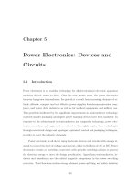
Layout Considerations (for Flyback Convertor)
Figure
17 Layout
Considerations
for
FSDZxO using
7DIP
15
Appendix C Fairchild Specifications
for
FSD210
and
FSD200
267
7-DIP
762
TIP
1762.0251
268
Appendix
C
Fairchild Specifications for
FSD210
and
FSD200
Package
Dimensions
(conmedi
7-LSOP
FSDZIO.
FSD200
17
Appendix
C
Fairchild Specifications for
FSD210
and
FSD2OO
269
Product Number
[
Package
1
Rating
FSOZIO,
FSOZW
Topr ('c)
Ordering Information
FSD2lO 7DIP 700V.
0.5A
I
-25°C
to
+85"C
FSD210M
DISCLAIMER
FAIRCHILO SEMICONDUCTOR RESERVES THE RIGHT
TO
MAKE CHANGES WITHOUT FURTHER NOTICE
TO
ANY
7LSOP 7wv.
0
5.4
PRODUCTS
HEREIN
TO IMPROVE
RELIABILITY
FUNCTION
OR
DESIGN FAIRCHILD
DOES
NOT
ASSUME ANY
LlABlLlTYARiSlNG OUT
OF
THE APPLICATION
OR
USE
OF
ANY
PRODUCT
OR
CiRCUlT DESCRIBED HEREIN, NEITHER
DOES
IT
CONVEY
ANY LICENSE UNDER ITS PATENT RIGHTS, NOR THE RIGHTS
OF
OTHERS
LIFE SUPPORT POLICY
FAiRCH LO
S
PRODUCTS ARE hOT AUTnORlZED
I
OR USE
AS
CR TICAL COMPONEhTS
ik
LiFF SUPPCRT OEViCFS
OR SYSTEMS WITHOUT IHE EXPKESS WHITTEN AI'PROVAL
OF
THF PRES DFNT
OF
FAIRCrliLU SEM CONDLCTOR
CORPORAT ON
As
Lie:
here
r
1.
Life support devices
or systems
are devices
or
systems
which.
(a)
are
intended
for
surgical implant
into
me body.
or
(b)
support
or
sustain
life,
and
(c)
whose
failure
to
perform
when
propedy
used
m
aacardance
with
inslruchons
for
use
provided in the labeling.
can
be
reasonably expected to result in
a
significant injury
of
the
Usel
2.
A critical component in any camponant
of
a life
support
device
or
system
whme
failure
lo
perform
can
be
reasonablyexpectedlocauJBthefadur~afthe
iifesupport
device
or
svstem.
or
lo affect its safetv
or
effectiveness.
w
fslrcnlsem,.un
4#2Dm5
D
Om
001
,
2004
Faimbld
SemlumOuc10(
C~iporaUm
This Page Intentionally Left Blank
27
1
272
Appendix
D
Fairchild
Specifications
for
FAN5307
-
FA1
RCH
ILD
-CO”
www.fairchiIdserni.com
FAN5307
High-Eff iciency Step-Down DC-DC Converter
Description
h
IC.id
\lI
I’
1\38
.
Typical Application
REV
1
0
1
2/4/04
Features
-
95%
Efficiency. Synchronous Operation
*
Adju\tahlr Output Vbltage Option from
0.7V
10
VIR
-
?.SV
to
5.5'4
Input
Voltage
Range
*
Cu\ti~mzcd
Fixed
Output
Voltage
Optiirni
-
Up
to
3UOrnA Output Cumnt
*
Fixed Frequency
IMHL
PWM Operation
*
High
hfilciency
Power
Stwr
Mode
-
100%
Duly Cycle
Low
Dropout Opcrirtioti
-
Suit
Start
-
Dynamic Output
Voltage
Positioning
*
15pA
Quiescent
Currenl
*
Excellcnl
Lmad Tnmient Ke\ponsc
.
5-Lead
SOT-21
Package
-
6-Lead
M1.P
3nlmm
h'ackngc
Applications
-
P<rket
Ks,
PDA\
*
Cell
Phone5
*
Battery-Powered Pwtahle
Devices
*
Digital
Camcms
*
Low
Power
LISP
Suppile\
Description
The
FANS307,
s
high efficiency
low
inoisc
\ynchronous
PWM
current
mode
and
Pulx
Skip
(Power
Save) mode
DC-DC convener is
devigned
for baltery-powered applica-
tion,.
It
provides up
to
300niA
of
output
current
ovcr
il
wide
input
range
fmm
2.5V
to
J.5V.
The
output
volt~ge
can
he
either
internally
fixed
or externally adlustable
o~er
a
wide
range
of
0.7V
to
5.5V
by
ao
external
voltqe
dividtr. Cusloni
wtpnt
vollages
are
iilw
awihhle
At
malerate
and light
loads
pulse
skipping modulation
is
used.
Dyniiinic
voltage po\moning
15
applied. and the output
volmge
is
\hifted
0
8%
above noniiniil value
for
mcrersed
hcadmom
during
load
lransient*.
At higher
loads
the system
imtonratically switchm
to
currcnl
inode
PWM
contiol.
operating
at
I
MH,.
A
current
inlode
cuntnil
loop with
Iaht
trilnvcnt rcrponsr
cnwres
excellent
line
md
load
regulation
In
Po-er
Saw
iniode.
the
quir*cent
current
1,
reduccd
to
I5pA
in
urdcr
to
achieve high efficiency
and
lo
rncuir
long
battery
life
In
5hut-dawn
niodr,
thc
wpply
~urrcnf
drop,
helow IpA.
The
device
i\
availilble
nn
J-lead
SOT-23
dnd
6-lend
MLPIx3mm
package.;
Appendix
0
Fairchild Specifications for FAN5307
273
Pin No. Pin Name Pin Description
1
2
GND Ground
3
4
~~~~
.
VIN Supply voltage input
~~
EN
FB
Enable Input. Logic high enables the chip and logic low disables the chip and reduces
Feedback Input
In
case of fixed voltage options. connect this pin directly to the output
supply current to
<1
pA
DO
not float this pin
For an adlustable voltaoe ODtiOn. connect this Din to the resistor divider
PRODUCT SPECIFICATION
Pin
No.
1
2
3
4
5
6
Pin Assignment
Pin Name Pin Description
EN
Enable Input Logic high enables the chip and logic low disables the chip and reduces
supply current to itpA Do not float this pin
GND Reference ground
VIN Supply voltage input
~~~~
Lx
Inductor pin This pin
16
connected to the internal MOSFET switches
PGND
FB
Power ground Internal N-channel MOSFET
IS
connected to this pin
Feedback Input In case of fixed voltage options, connect this pin directly
to
the output
For an adjustable voltage option. connect this pin to the resistor divider
TWVIEW
S-bd
Yn-23
FAN5307IFAN5307SX
FAN5307
~
Topvim
".
5
~ Lx
i
Inductor pin Thls pin is connected to the internal MOSFET switches
274
Appendix
D
Fairchild Specifications for
FAN5307
PRODUCT SPECIFICATION
FAN5307
Absolute Maximum Ratings
Parameter
1
Min
1
Max
I
Unit
V,.,
1
-03
1
65
1
V
Voltage
on
any other pin
Power Dissipation (Continuous. at
TA
=
25C)
Lead Soldering Temperature
(10
seconds)
Storage Temperature
Electrostatic Discharge
(ESD)
Proleclion Level (Note
2)
~~~____~
~
____~~~
CDM
Recommended Operating Conditions
Noles:
1
Derale
above
25C at a rate
of
3YCN
2
Using
Mil
Std
883E.
method
3015
7(Human
Body
Model) and EINJESDZZC101-A (Charge
Devlce
Model)
3
Refer
lo
the
applications
section
for
further
delaiis
REV
1
0
1
2/4/04
Appendix
D
Fairchild Specifications for FAN5307
275
Parameter
I
Conditions
I
Min.
FAN5307
-
-~
.~
~~~~ ~ ~ ~~~ ~~
PRODUCT SPECIFICATION
General Electrical Characteristics
ViN
=
2
5V to 5 5V. loUT
=
200mA.
EN
=
VIN, CiN
=
4
7pF. Cour
=
22pF,
Lx
=
10pH.
TA
=
-4OC
lo
+85"C. unless
ofhewise noted Typical values are at
T,
=
25°C
Typ.
1
Max.
1
Units
Load Regulation
6-Lead
3x3mm
MLP
Load Regulation
Feedback (FB) Voltage
I
05
I
Reverse Leakage Current into pin
SW
v
=
5 5v
VIN
= Open.
EN
=
GND.
V
v,,
=
2
5
to
5 5v
(6
Lead
3x3mm
MLP)
omA
c
louT
s
300rnA
4
REV
1
0
1
214104
276
Appendix
D
Fairchild Specifications for FAN5307
FAN5307
PRODUCT SPECiFiCATION
Electrical Characteristics for Fixed VoUT
=
1.8V Version
VIN
=
2
5V
to
5 5V.
loui
=
200mA. EN
=
ViN. CiN
=
4
7pF,
C,,,
=
22pF,
Lx
=
10pH.
TA
=
-40C
to
+85"C. unless
otherwise
noted
Typical values are
at
TA
=
25C
1
93
Note
4
Transition
voltage
1s
defined
as
the
dlnerence
between
the
output
voltage
measured
at
0
lm
A
(PFM
mode) and
3nnmA
(PWM
mode) respectively
5
6
These
Iim115
a150
apply
lo
any
mode
transition
caused
by
any
klnd
of
load
lransmon
within
specified
output
current
range
REV
I
n
t
214104
5
Appendix
D
Fairchild Specifications for FAN5307
277
PRODUCT SPECIFICATION FAN5307
~~
Typical Performance Characteristics
Inmi
6
REV
1
0
1
Z4104
278
Appendix
D
Fairchild Specifications
for
FAN5307
'%
LOOIC
CONTROL
il
Detailed Operation Description
The FAN5307 is
a
atep-down convener
operatrng
in a
current-mode PFMPWM architecture with
a
typlcal switch-
ing frequency
of
IMHr.
At
moderate to heavy loads, the
con-
verter operates in pulse-width-modulation
(PWM)
mode. At
light load, the
converter
enters
a
power-save mode (PFM
pulse skipping) to keep the oiliciency high
PWM
Mode
In
PWM
mode.
the device opcrater at a fined frequency of
IMHr.
At the beginning of each clock cycle, the P-channel
tmnwtor
1s
turned
on.
The inductor current
ramp*
up
and
i\
monitored via
an
internal circuit.
The
Pshannel witch ir
turned off when the \ensed current causes the PWM compar-
itor to tnp when the output voltage
IS
in regulation
or
when
the inductor current reaches the current limit (set internally
10
typically
520mA).
After
a
minimum dead time the N-
channel transistor is turned
on
and
the inductor current
ramp
down. A\ the clock cycle is completed, the N-channel witch
1s
turned
off
and
the next
clock
cycle
sms
PFM
(Power
Save)
Mode
A\
the
load
current decreases
and
the peak mductoi current
no
longer reaches the typical threshold
of
80mA.
the
con-
vener enters
pulse-irequency~modulation
(PFM)
mode
In
PFM mode the device operates with
a
variable frequency and
constant peak current thus reducing the quiescent current to
minimum. Consequently.
the
high efficiency is maintained
ill
light loads, As
soon
a$
the
output voltage
fiillr
helow
a
threshold. set
at
0 8%
ahove the nominal
value,
the P-channel
tran\istor is turned
on
and
the
inductor current
ramps
up
The P-channel witch turns
off
and the N-channel turns
on
as
thc
peak
inductor current
is
reached (typical
140mA)
The N-channel transistor
IF
turned
off
before
the
inductor
current hecwnes negative. At this lime the P-channel is
switched on again starting the next pulre.
The
converter
continues these pulses until the high threshold (typical
1.61
rbow
nominal
value)
is
reached
A
higher output
valtilge
in
7
REV.
1
0
I
2/4/04
Appendix D Fairchild Specifications for FAN5307
279
PRODUCT SPECIFICATION
PFM
mode give- additional headroom
for the voltage
drop
during
a
load
transient
from
light
to
full
load. The voltage
overshoot
during
this
load
tranarent
ib
also
rninmmired
due
to
active
regulation
during turning
on
the
N-channel
rectifier
switch The device stay, in
sleep
mode
until the output
voltage
Blls
below
the
low
threshold. The
FAN5107
enten
the PWM
mode
8s
soon
as
the wiput
valtage
can
no
longer
he regulated
in
PFM
with
comtant
peak
current
100%
Duty Cycle Operation
A\
the
input voltage approaches
the
output voltage and the
duty cycle
exceeds
the typ~cal
95%.
the
cunverter
turns
the
P-channel
transistor
continuously
on.
In
thia
mode
the
output
voltage
is
equal
to
the
inpur
voltage
minus
the
vultage
drop
across the P-channel transistor.
VOUT
=
Vt,
-
ILO*D
x
(Rd.0~
+
RL),
where
RdtON
=
P-chdnnel
switch
ON
IS\NIIICZ
IWA"
=
output
CUrrent
R,,
=
Inductor
DC
IIIIUBIICI
FAN5307
son
start
The
FAN5307
has
dn
interindl
sofl-\tart circuit that
limits
the
inrush
current during slam-up. This prevents
pwible
voltage
drop,
of
the mput
voltage
and
eliminates the output voltage
overshoot
The
mtt-&xl
i\
implemented
a\
a
digital
circuit
increasing
the switch
cumnt
in
four
\teps
to
the
P-channel
current
limit
(520rnA)
Typical
start-up
time
fur
a
IOpF
out-
put capacitor
and
n
load
current
of
2WmA
IS
500p\.
Short-circuit
Protection
The
swilch peak
cumnt
L
limited
cycle hy
cycle
to
a
typical
value
of 520mA.
In
the event
of
a
output
voltage
short circuit
the
device
uperatea
ai
minimum
duty
cycle,
therefore
the
average input current
ii
lypically
IOUmA.
REV. 1
.O
1
2/4/04
280
Appendix
D
Fairchild Specifications
for
FAN5307
Inductor Vendor
Value
FAN5307
Part Number Performance
PRODUCT
SPECIFICATION
6
8pH
1
OvH
Application Information
Adjustable Output Voltage Version
Thc
output
solrage
for
the
adjustable
version
is
he1
hy
the
external
rc\~stor
dirider,
:I\
shown
bclow
CDRH5D18-100
Efficiency
CDRH4D28-100
Murata LQH66SN100M
OIL
Sumida CDRH3D16-6R8 Smallest
CDRH4D18-100
SoiUtlon
CR32-100
CR43-100
Murata LQH4C100K04
V<,,
=
osv
x
I
+
c
21
10
reduce
noise cenritiuity.
RI
+
R2
should
not
exceed
800kR
Inductor Selection
The
inductor pariinictcr\
direcily
related
to
device
perfot-
mances
are
satoration
c~rrent
and
dc
resi\tmce
The
kAN5307
operdle,
with
a
typical
inductor
value
01
IOpH
The
Ioivm
the
dc
resimtance,
the
higher the
efficienq.
For
iafuritioii
current.
the
inductor
\hould
he
rmd
hiphcr
than
the
mtixiniurn load
current
plu,
half
,it
the
inductor
npple
current
that
i\
calculated
a\
tollowa:
wherc.
I
=
Switching
t.rrquenq
L
=
Inductor
Vdue
AI,
=
Inductor
Ripple
Current
Table
1:
Recommended Inductors
Input Capacitor Selection
Foor
best
pcrhrrnance.i.
a
low
ESR
iiiput
capacitor
is
requ~rcti.
A
ceramic
cilpicitor
of
at
least
4.7pF.
placed
.is
clwe
to
he
input
pin
oi
the
device
IS
recornntcnded.
Output Capacitor Selection
The FANS107's
\=,itching
trequency
of
IMHi
~llow\
the
use
of
a
low
ESK
cerdrnic
capacitor
with
il
value
of
lOpF
10
22pF.
Thir
provider
low
output
boltape ripple.
In
power
save
imodr
the
output
wllage
ripple
IS
independent
of
the
output
~pacitor
villue
and
thc
ripple
ib
determined
hy
the
internal
comparator
threshuld\.
The
typical output
voltage
ripple
at
light
laid
15
1%
of
the
inoimnrd
output
voltage.
1
CaDacitor
1
Vendor
1
PartNumber
I
value
4.7pF Taiyo JMK212BY475MG
JMK316BJ106KL
C1201ZX5ROJ106K
C3216X5ROJ106M
22uF Murata GRM32DR60J226K
Table
2:
Recommended Capacitors
PCB Layout Recommendations
Thc inherently high
vdk
currents
and
witching
frequency
rrf
the
power
wpplia
require
il
ciirdul
PCB
Ir)ou~
deiign.
Theretore,
use
wde
inccs
for
the
high
cumnt
path
awl
pl;icr
the
input
capacitor.
the
inductor.
and
the
output
capaci-
tor
a,
cIo\c
a\
powblc
to
the
megrated
circuit
terminuls.
bar
the
adjuclable
%enion
the
resistor dividcr \hdd
he
m111cd
sway
from
the
inductor
to
iivriid
elcctrnnuignetic
intrrfer-
encc.
The
6-leiid
M1.P
\ervon
ut
the
IAN5307
5eparata
the
high
currcnt
ground tmm
the
reference
ground.
therefore
it
i\
niom
tolerant
the
PCB
layout
devgn
snd
\hua\
hettcr
pcr-
formance
REV
1
.O
1
214104
9
Appendix
D
Fairchild Specifications
for
FAN5307
281
PRODUCT SPECIFICATION
~~
Mechanical
Dimensions
&Lead
3x3mm
MLP Package
2x
TOPVIEW
O2MIN
BOTTOM VIEW
NOTES
RECOMMENDED LAND PATTERN
FAN5307
~
10
10
REV
1
0
1
2/4/04
282
Appendix
D
Fairchild Specifications for
FAN5307
Symbol
FAN5307
PRODUCT
SPECIFICATION
Inches
1
Millimeters Notes
Mechanical Dimensions
5-Lead SOT-23
Package
Notes:
1
Package outline exclusive
of
mold flash
a
metal burr
2
Package outline exclusive
of
solder plating
3
ElAJ
Ref Number
SC-74A
REV
1
0
1
214104
11
Appendix
D
Fairchild Specifications for FAN5307
283
Product Number
VOVT (V)
1.8
1.8
Adlustable
Adlustable
FAN5307
-
PRODUCT SPECIFICATION FAN5307
PackageType Order Code
5-Lead SOT-23 Tape and Reel
6-Lead
3x3mm
MLP Tape and Reel
5-Lead SOT-23 Tape and Reel
6-Lead 3x3mm MLP TaDe and Reel
FAN5307S 18X
FAN5307MP18X
FAN5307SX
FAN5307MPX
Ordering Information
DISCLAIMER
FAIRCHILD SEMICONDUCTOR RESERVES THE RIGHT TO MAKE CHANGES WITHOUT FURTHER NOTICE TO
AhY PRODUCTS rlFRF N TO MPROVt
Ht-
AB
L
TY
FLhCT ON OH
DtS
GN FA RCr?
-D
DOES hOT ASS,ME
Ah< AB
hE TrlER DOFS
T
LONdFY AhY XLNSE LhDER
TS PATFhT RlG?lTS hOH
T?!E
R
GirTS
OF
OThERS
TY
AH SlhG OLT OF THE APPL CAT Oh
OH
LSE OF AhY PRODLCT
OR
C RCL T DESCR
OEU
r3LHE.h
LIFE SUPPORT POLICY
FAIRCHILD
S
PRODUCTS ARE NOT AUTHORIZED FOR USE AS CRITICAL COMPONENTS IN LIFE SUPPORT DEVICES
OR
SYSTEMS WITHOUT THE EXPRESS WRITEN APPROVAL
OF
THE PRESIDENT
OF
FAIRCHILD SEMICONDUCTOR
CORPORATION As
used herein
1
Life
suppon devices
01
systems
are
devices
or
syslems
2
A
~rltl~al
component
m
any component
of a
life suppan
which (a)
are
intended forsurgical implant
into
the body
or
device
or
System
whose
failure
to
perform can he
(b)
suppon
or
sustain
life and
(c)
whose
failure
lo perform reasonably expected to
cause
the
failure
of the life support
when properly used
m
accordance wlth ~nstrualons
for
use
device
01
system
or
to anect
its
safety
or
eflectweness
provided
in
the
labeling can
he reasonably expected lo
result
in
a significant
inpry
of
the
user
www fairchildsemi cam
This Page Intentionally Left Blank
285
286
Appendix
E
Fairchild Specifications for
ACE1502
-
October
2002
FA1
RCH
I
LD
ACE1
502
Product Family
Arithmetic Controller Engine (ACExTM)
for Low Power Applications
General Description
The ACEtY)2 (Arithmetic
Controller
Engine)
hmily
01
morocon-
trollers
15
a
dedicated pragrammable monolithic integrated
circuit
lor
applications
requlrtng
high
pedormance.
Ihv power. and
Small
size
I1
IS
a
lully
~talic
part
fabricated using CMOS
IRhnology
The ACE1502 product
lamily
has an
8
bit
miCrocOntrOller
core.
Ed
bytes
01
RAM,
Ed
bytes
01
data
EEPROM
and
2K
bytes
01
code EEPROM
Its
on-chip peripherals
include
a
multilUnCtiOn
t6~bit
timer,
a watchdog/idle
timer. and
piqrammable
under-
voltage detection
circuitry
On-chip Clock
and
reset
1unct~ons
reduce the
number
01
required
external
components The
ACE1502 product
family
15
available
in
8-
and
14-pin SOIC.
TSSOP
and
DIP packages
Features
8
Arilhmetc
Contioller Engine
8
2K
bytes
on-board
code
EEPROM
8
64
bytes
data EEPROM
8
64 bytes RAM
8
Watchdog
8
Multi-input wake-up on all eight general purpose
110
pins
8
16-bll
multifunction
timer
Wlth
dinereme capture
8
Hardware Bit-Coder
(HBCI
8
On
Chip
o~~illatoi
No
external
components
tp5
instruction
cycle
time
i1
2%
accuracy
8
InSlluctlOn
set
geared
lor
block encryption
8
On-chip
Power
on
Reset
8
Programmable
read
and
write disable l~nctlons
8
Memory mapped
110
8
32
level
Low Voltage
Detection
8
Brown-out
Reset
8
Sonware
selectable
110
option
-
Push-pull outputs with
in-stele
oplion
-Weak pull-up
or
high impedance ~nputs
8
Fully ~talic CMOS
-
Low power HALT mode (100nA
0
2
7Vl
-
Power saving IDLE mode
-
t
8-3
6V
8
Single supply operation
40
data
leten~l~n
t
6V
data
EEPROM
min
writing voltage
8
1.OOO.OW
data changes
8
8
and
14-pr SOIC TSSOP
and
DIP packages
8
In-circuit proorammino
Block and Connection Diagram
VCC'
u
02002 Fairchild
Semiconduclor
Corparation
1
ww
lslrchildreml
Corn
ACE1502 Product Family
Rev
I
7
Appendix
E
Fairchild Specifications
for
ACE1502
287
Figure
2.
ACEx Application Example (Remote Keyless Entry)
I
"CC
A
Figure
3.
ACE1502 &pin SOiC and DIP Device Pinout
a) Normal Mode Operation
b)
Programming Mode Operation
SFT-IN
LOAD
iFl
VCC
GND
G3 G4
4:
L
2
t
2
G5
G2
NCNCC
SFT-OUT
GO
5
GI
NC
4
5
3
CKi
Figure
4.
ACE1502 &pin TSSOP Device Pinout
a) Normal Mode Operation
GND
vcc
471
z:
b)
Programming Mode Operation
ti:
471
Zr-OUT
G3 GO
LOAD
NC
G4
4 G5 SFTLIN 4
5
NCNCC
Figure
5.
ACE1502 14-pin SOiC, TSSOP and DIP Device Pinout
a) Normal Mode Operation
b)
Programming Mode Operation
NC NC
G6
G2
NC
SFT-OUT
NC
NCNCC
NC
288
Appendix
E
Fairchild Specifications for
ACE1502
Part Number
~
Operating Voltage
ACE1502E
tppy3rpp
~
1
18103GV
~~~
ACEt502V
2.
Electrical Characteristics
7
Ambient Operating Temperature
-40
c
10
+85
c
40Ct01125C
~ ~~ ~
~-
~~p-~~-p~
~ ~ ~
ACE1502 DC Electrical Characteristics,
vcc
=
1
8
lo
3
6V
All
rneasurernenfs are valid for arnbienl operating lernperature unless otherwise slated
3
www
lalrcn,ldse"l,
corn
ACE1502
Product
Family
Rev
1
7
Appendix
E
Fairchild Specifications
for
ACE1502
289
I
Parameter Conditions
MIN
TVP
MAX
Units
setpolnt
internal
Clock
frequency
varlallon
Crystal
OEClllatol
frequency
External
Clock
treauencv
1
6V
to
3
6V
al
constant
temperature
1
SV
lo
3
6V
at
t~ll
temperature
range
(Note
61
6
'0
25
MHz
(Note
51
1NOte
51
6
MHI
12
-
~.
~
5
Tnr
pPlm,ma,~lrPo,,erliy,,~"a,an,e~d~"4~r,yn
bills"",
IW~olnle"
6
Tnr
Da,lmp,el
rlalal,r,,,LC
IX,,
,?
,101
,a/_
lSStD"
rOn,ar,
//,rLn,,"
10,
add,l,Dnd# ’llarac1sI,>*I~"II
oat1
ACE1 502 Electrical Characteristics for programming
All
data valid at ambient temperature between 3 OV and
3
6V The following characteristics are guaranteed
by design but are not
100%
tested See "EEPROM write time"
In
the AC Electrical Characteristics for
definition of the programming ready time
O~c~llafor
start
up
time
INole
61
2400
cycles
4
www
lalrCnlldseml
corn
ACE1502
Product
Famliv
Rev
1
7
Parameter Conditions
MIN
TYP
MAX
Units
LBD
voltage
Inieshold
vaiation
40
C
to
165
C
5
15
Parameter Conditions
MIN
TVP
MAX
Units
290
Appendix
E
Fairchild Specifications
for
ACE1502
AC
&
DC Electrical Characteristic Graphs
Figure
6.
Internal
Oscillator
Frequency
The
graphs
m
this
seclion
are
lor
design guidance
and are
based
on
p<el#minary
lest
dala
lnlsrnal
O~lclllalor
Frequency
vs Tcrnprafure
201,
I
I
0 0
25
85
125
I93L
Ternpruure
[
C]
Figure
7.
LBD
and
BOR
Threshold Levels
BOR
La".,,