MANAGING POWER ELECTRONICS VLSl and DSP-Driven Computer Systems phần 9 doc
Bạn đang xem bản rút gọn của tài liệu. Xem và tải ngay bản đầy đủ của tài liệu tại đây (1.84 MB, 41 trang )
Appendix
E
Fairchild
Specifications for ACE1502
307
Bit7 Bit6 Bit
5
Bit
4
1
Bit3
Figure 27. Multi-input Wakeup (MIW)
Block
Diagram
Bit2 Bit1 Bit
0
I
0.8.
61%
I
Configuration Bit Data Bit Port Pin Configuration
0
0
High-impedence
input
(TRI-STATE
mputl
0
1
Input
with pull-up (weak
One
Input]
1
0
Push-pull
zero
output
1 1
Push-pull
one
output
~~~
~~
WKEDGiO 71 WKPNDlO
71
10
WIINTEN
81
lolTcCNIAL
9.
110
port
The eight
110
pins
Ism
an
B-pin
package
option) are bi-
directional
(see
Figure
28) The b~-d~recl~anal
110
pins can be
individually conligured by
solware
to
operate as high-
impedance ~nputs.
as
inputs
with
weak
pull-up,
or
as
push-pull
outp~ls The
operating
state
IS
determined by the
content5
01
the corresponding blts
I"
the data and
conllguratlon
reglrters
Each
bl-directional
110
pin
can be used
tor
general purpose
110,
or
8n
some
cases.
tor
a Specific
alternate
Iun~tion
determined
by
the an
chip
hardware
Figure 28. PORTGD Logic Diagram
T
GXPULLEN ~
GXBUFEN ~
GXOUT
____
GXlN
+
Fiaure 29.
UO
Reaister bit assianments
9.1
I/O
registers
The
110
pins
(GO-G7) have three
memory~mappsd
port
rega-
ters
associated with the
110
circuitry
a port
configuration
iega-
ter
(PORTGCI. a port data
register
IPORTGD).
and
a
port input
register (PORTGPI PORTGC
1s
used to
configure
the pins
as
inputs or
outputs
A
pln
may
be
contlgured
as
an
mput
by
wrltlng
a
0
or
as
an
output by writing
a
1
to 81s
corresponding PORTGC
bit
If
a pin
IS
configured
a5
an
output.
1s
PORTGD bit repre-
sents
the stale
01
the
pin
(1
=
logic high. 0
=
logic
low1
It
the pin
IS
configured
as
an input.
Is
PORTGD
bit
selects whether the
pin
1s
a
weak
pull-up
or
a
high impedance input Table
13
pro-
vides
detats
of
the
port
cont~ural~olon
oplions
The port
configu-
ration
and
data
reglslers can both
be
read
from
or
wrlnen
lo
Reading PORTGP
returns
the
value
01
the pan plnr regardless
01
how the plns are
contlgured
Since
this device LUppOnS MIW.
PORTG
inputs have
Schmin
triggers
22
w
la,rchl,drem,
corn
ACE1502 Producr Family
Rev
1
7
308
Appendix E Fairchild Specifications for ACE1502
Bit Number
bits
31-30
bit
29
bit 28
bits
27-25
bit
24
bitS23-I9
bits
18
-8
bllS
7-0
10.
In-circuit Programming Specification
The
ACEx
microcontroller
supports
n
CirCUit
programming
Of
the
internal
data
EEPROM
code
EEPROM
and
the
nlllalll.9
t,on
ieg,sters
in
order
ID
enter
lnto
program
mode
a
10
bt
opmde
(0x340)
must
be
shAed
8nto
the
ACE1502
whlle the
devlce
IS
executlng
the
internal
power
on
reset
ITRESET) The
shining
protocol
101
lows
the
same
timing
rules
as
the programming
prot~col
defined
m
Figure
30
The opcode
15
ShAed
into
the
ACE1502
serially
MSB
11151
Wlth
the
data
being
valid
by
the
rlsing
edge
01
the
clock
Once
the
pattern
IS
Shined
~nto
the
device
the
current
10
blt
pattern
1s
matched
lo
pro1ocoI
entrance
opccde
of
0x340 If
the
10
bit
pattern
85
a
match
the
devlce
will
enable the
lnternal
program
made
nag
SO
that
the
aevlce
WIII
enter
mo
program
mode
once
reset
has completed
(see
Figure
30
)
The
apcade
must
be
ShiHed
m
aller
Vcc
Eenles
to the nominal
lwel and Should
end
before
the
power
0"
reset
sequence
(T,,,,,)
c~mpletes
othewlse the
devlce
wlll
Start
normal
execution
01
the program
cde
If
the
external
reset
IS
applied
by
bnngmg
the
reset
pin
tow
once
the reset
p1n
IS
release
the
opccde may
now
be
ShlHed
m
and
agaln should
end
before
the
reset
sequence
CompleteE
10.3 Programming Protocol
AHet
placing the device
~n
program the programming protocol
and commands
may be Issued
~n externaiiy
controiiea
IOU
w~re
medace
conststlng
01
a
LOAD
control
p,n
(~3)
a
sertai
data
SHIFTIN
,"put p~n
(G~I
a serial
data
SHIFTOUT
output
p~n
(GZ)
and
a
CLOCK
pn
(GI)
IS
used
to
access
the
on
chip
memory
lo~ation~
Communoauon
between the
ACEx
miCiOCOntroller
and the
external
programmer
8s
made through
a
32
bvt
command
and
response
word
descnbed
8n
Table
14
Be
Sure
to
either
float
01
tle
G5
to
Vcc
lor proper programming
lunctionalihl
The
~enal
data
timing
lor
the
lour
wlre
lntedace
8s
shown
8n
F8g
we
31
and the programming protocol
15
shown
In
Figure
30
10.3.1 Write Sequence
The
external
programmer
brings
the
ACEx
mlcroconlroller
Inlo
programming then
needs
to
set
the
LOAD
p1n
lo
VcC
before
Shining
$n
the
32
bit
serial
command
word
using
the SHIFT
IN
IS
ShiHed
8n
Drst
At
the same
time
the
ACEX
mlClocOntrOllel
shifts
out
the
32
bit
Serlal
response
lo
the
last
command
on
the
end
CLOCK
stgnats
BY
aetlnitlon
blt
31
01
the command
word
Table 14 32-Bit Command and Response Word
lnput Command Word
set
to
I
to
readiwme data
EEPROM.
or
the
~nii~ai~mon
x
Must
be
sef
lo
0
regsters.
OlherWSe
0
Set to
1
to
readiwnte
code
EEPROM,
Olhewme
0
Must
be
set to
0
X
X
X
set
to
I
to
read.
o
to
wr~te
Must
be
set
to
0
Address
of
the
byie
to
be
read
Or
written
~ata
to
be
X
X
Same
as
lnput
Command
word
Programmed
data
or
data
read
at
speclfled
address
01
zero
81
data
1s
to
be
read
SHIFT
OUT
pin
It
1s
recommended that the
external
program
mer
samples lhlS
signal
t
ACCESS
(500
ns)
aher
the
ming
edge
01
the
CLOCK
slgnal
The
se1881
response
word.
sent
immedi
ately
aner
entering
programming mode
contains
indeterminate
data
AHer 32
b!ls
have
been
ShiHed inlo
the
device.
the
external
pro-
grammer must set the
LOAD
slgnal
to
ov,
and then apply two
clock pulses
as
Shown
#n
Figure
30
to
complete
program
cycle
The SHIFT
OUT
pin
acts
as
the
handshaklng
signal
between
the
device
and
programming hardware
once
the
LOAD
slgnal
IS
brought
low
The
device
$115
SHIFT-OUT
low
by the
time
the
programmer has
sent
the
second
mng
edge
during
me
LOAD
=
0V
phase
Ill
the timing spec111calions
m
Figure
30
are
obeyed/
The
devlce
wlll
set the
R
bit
Of
the
Status
reglster
when the
wrlle
operation
has completed The
external
programmer
must
wall
lor
the SHIFT-OUT
p1n
lo
go
high
before
bringing
the
LOAD
$19-
nal
to
Vcc
lo
inifiate
a
normal
command
cycle
10.3.2 Read Sequence
When
reading
the
device
aher
a
wrlte.
the
external
programmer
must set the
LOAD
slgnal
to
Vcc
before
11
send5
the
new
com
mend
word
NUI,
the
32-btt
serlai
command word (for during
a
READ)
Should
be
mHed
inlo
the device
using
the
SHIFT-IN
and
the
CLOCK
slgnals
while the data
from
the prev10uS Com-
mand
IS
~erlally
shdled out
on
the SHIFT-OUT
pln
AHer
the
Read
command
has
been
Shilled
into
the device. the
external
programmer must.
once
again. set the
LOAD
signal
to
OV
and
apply two
clock
pulses
a5
Shown
in
Figure
30
to
complete
READ cycle Data
from
the
Selected
memory
location.
will
be
latched
tnto
the
lower
8
b15
01
the command
Word
shortly
aHei
the
second
rmg
edge
ot
the
CLOCK
slgnai
Writing
a
sene$
of
bytes
to
the
device
85
achleved
by sending
a
series
of
Write command
words
while
observing
the
devices
handshaklng requirements
Reading
a
series
01
byies
from
the
devce
15
achleved by
send-
mg
a
series
of
Read
command
words
with the
desired
addresses
8n
sequence and
readlng
the
lollowlng
response
words
10
ve@
me
correct
address
and
data
contenis
The addresses
of
the data
EEPROM
and
ccde
EEPROM
locatioos
are
the
-me
as
those used
8n
normal
operation
Power,ng
down
the device
will cause
the part
to
exit
program-
ming mode
Output Response Word
ACEI~OZ
product
Family
~ev
I
7
Appendix
E
Fairchild Specifications
for
ACE1502
309
YCC
,
~
~.
-
1
~~ ~ ~
RESET
LOADIGJ,
I
I
8
I._
, A
I
I
-
to
RESET
logic
ACE1502 Product Famitv Rev
1
7
310
Appendix E Fairchild
Specifications for
ACE1502
11.1
Brown-out Reset
The
Brown-out
Reset
(@OR)
function
IS
used
to
hold the
device
ln
reset
when Vcc drops
below
a
flxed threshold
(1
83V) Whlle
in
reset
the device
IS
held
8n
its
initial
Condition
until
Vcc
rises
above
the thieshold
value
Shortly
aHer
Vcc
rises
above the
threshold
value
an
internal
ieset
sequence
1s
started AHer the
reset
sequence
the
core
telches the
first
inst~uct1on
and
starts
The
@OR
Should
be
used
in
s~tuat~ons
when
Vcc
rises
and
falls
slowly
and
r
situations
when Vcc does
not
fall
to
zero
before
rising
back
to
Opelatlng
range
The
Blown-Out
Reset can
be
thought
of as
a
supplement function
to
the
Power-on
Reset
if
normal
operatIan
Vcc
does
not
tall below
-1
5V The Power-on
Reset
CI~CUI~
Works
best
when Vcc
stms
from
zero
and
rises
Sharply
In
appl~ca-
110115
where
Vcc
Is
not
constant.
the
@OR
will
give
added device
stability
The
@OR
cilcult
must
be
enabled through the
@OR
enable
bit
(BOREN)
in
the
~nitial~zat~on
register
The BOREN
bit
can
only
be
set
white the device
is
in
programming mode
Once
set
the
0OR
will
always
be powered.up enabled
SoHware
cannot dis-
able
the
@OR
The
@OR
can
only
be disabled
in
programming
mode
by
leSettlng
the
BOREN bit
as
tong
as
the
global
write
protect
IWDISi
feature
85
not
enabled
Figure
33.
BOR
and
POR
Circuit Relationship Diagram
i"3
11.2
Low Battery Detect
The Low Battery
Detect
(LBD)
circuit
allow5
soltware
to monitor
the Vcc
level
at
the
lower
voltage
ranges
LBD
has
a
32-1eveI
sonwdie
progidmmable
voltage
reference
threshold that
can
be
changed
on
the
fly
Once
Vcc
fa115
below
the
selecled threshold
the LBD
flag
in
the LBD
conti01
register
IS
set
The L0D
flag
will
hold
its
value
until
Vcc
rises
above
the threshold
(See
Table 15)
The
LBD
bit
IS
read only
If
LBD
15
0
it
indicates that the
Vcc
level
15
higher than the
Selected
threshold
If
LBO
is
1
11
indi-
cates
that the Vcc
level
IS
below
the
Selected threshold The
threshold
level
can
be
adjusted up
to
eight
levels
using
the three
trim
bits
(BLj4
O]]
01
the LBD
Control
register
The LBD
flag
does
not
cause
any
hardware actions
or
an
interruption
01
the
proces-
sor
It
IS tor
soHware
monitoring
only
The VSEL
bit
01
the L0D
~ontrol
register
can
be
used
lo
select
an external
voltage
SOUICE
rather
than Vcc
It
VSEL
15
1
the
voltage
source
lor
Ihe LBD comparator
will
tre
an
input
volfage
provided through
G4
If
VSEL
1s
0
the
voltage
source
will
be
VCC
The LBD
circuit
must
be
enabled through the
LBO
enable
bit
(LBDEN)
r
the
inil~at~~at~on
register
The LBDEN bit
can
only
be
set
while the device
8s
8n
programming mode
Once
set
the LBO
will
BIWIYS
be powered-up enabled
Sohware
cannot
disable the
LBD The LBD
can
Only
be
disabled
I"
programming mode by
resetting
the L0DEN
bit
as
long
as
the
global
write
protect
(WDIS)
feature
15
not
enabled
The
L0D
c~icu~t
15
disabled
during
HALT IDLE mode
AHer
exit-
mg
HALT IDLE
sohware
must
wail
at
lease
10
us
belore
read-
ing
the LBD
blt
to
ensure
that the
internal
c~rcu~f
has stabilized
25
www
la,rcP,~oiem#
cow
ACE1502 Product
Family
Rev
1
7
Bit7
Table
15.
LED
Control Register Definition
Bit6 Bit5
1
Bit4 Bit3
1
Bit2
1
Bit1 Bit0
ELI4
01
26 WWW falrchlldreml
Corn
ACE1502
Producl Family
Rev
1
7
VSEL
X
LBD
312
Appendix
E
Fairchild Specifications
for
ACE1502
1
12.
RESET
block
When a RESET sequence
IS
initiated
all
I10
regislers
will
be
reset
sening
all
llOs
to
high lmpedence inputs The
System
Clock
IS
restarted alter the
required
Clock
51all
up
delay
A resel
IS generatea
by
any
one
ot
the
t~ii~w~ng
four
ConaNttons
0
External
cryStallreSOnatoi
13.
Power-On Reset
The
Power-On
Reset
(POR)
ClrCUit
1s
guaranteed
to
Work
If
the
rate
01
rise
of
Vcc
85
no
slower
than lOms11voll
The
POR
clicuil
was designed
to
respond
to fast low to
high
tran~ition~
between
OV
and
Vcc
The
circult
wdI
not
work
11
Vcc
does
not
drop
10
OV
before the
next
power-up
Sequence
In
applications
where
11
Ihe
Vcc
we
is slower
than 1Om5/1
volt
or
2)
Vcc does
not
drop
Bit
7
Bit
6
Bit 5 Bit
4
14.
CLOCK
The ACEx
mi~roc~ntr~ller
has
an
on-board
05CilIatOl
trimmed to
a
frequency
of 2MHz Who
IS
dlvided
down
by
two
yielding
a
lMHz frequency
(See
AC Electrical Characleristosl Upon
power
up
the
owchip
05cillalor
runs
continuously
unless
enter
1ng HALT
mode
or
using
an
external
clock
Source
It
required.
an
external o~~lllator C$rcu11
may
be
used
dependlng
on
the
slates
01
the
CMODE
b8IS
of
the
lnltialllatlon
reglster
(See
Table
16)
When
the
devlce
15
dWen
using
an
external
clock.
the
clock
input
to
the
device
(GIICKI) can
range
between
DC
to
4MH2
For
external
crystal
conllguratlon.
the
output
Clock
(CKOI
1s
on
the
GO
pin
(Sea
Flgure
34
)
II
lhe devlce
is
conflg-
"red for an external square
dock
1
w4
not
be
divided
Table
16.
CMODEx Bit Definition
Bit 3 Bit
2
Bit
1
Bit
0
CMODE
[l]
1
CMODE
[O]
1
Clock Type
0
0
Internal
1
MHz clock
0
1
External square
clock
undefined
unaeflnea unaeilnea
undehed
undefined
unaeflned
E~DLE
EHALT
15.
HALTMode
The HALT
mode
15
a power saving
feature
that
almost
Corn
ptetely
Shuts
down
the
devlce
lor Current
~onservation
The
devlce
IS
placed
into
HALT
mode
by
Sening
the HALT
enable
bll
(EHALT)
of
the HALT
register
thmugh sonware
uslng
Only
the
cally cleared
upon
exiting HALT When
enterlng
HALT
the
lnlel
nal
os~illat~r
and
all
the
Owchip
systems
including
the LED
and
the BOR circu~ts are Shut
down
Fiaure 35.
HALT
Reaister Definition
"LD
M
#'
,nstr~ct,on
EHALT
IS
a wrlte
only
blt
and
1s
automati-
lo
OV
before
the
next power
up
sequence
the external
reset
option
Should
be
used
The
external
iesel
provides
a
way
10
properly
reset
the ACEx
miCrOCOntrOller
1
POR
cannot
be
used
8n
the
appli~alion
The
external
reset
pin
contain5
an internal
pull up
r8515tor
There
fore
lo reset
the
device
the reset p'n
should
be
held
low
for
at
least
2ms
so
that the
internal
Clock
ha5
enouah
time
lo
stabilize
Figure 34. Crystal
The
device
can
exit
HALT mode
only
by the MIW
C1rcu11
There-
tore.
prior
to
enterlng
HALT
mode
soltware
must
contlgure
the
MIW
circuit
accordingly
Gee
Section
81
Alter a
wakeup
from
HALT
a
tms
start-up
delay
8s
,mated
to
ailow
!he snternai
oscti-
lalor
to
Stabilize
before
normal
execution resumes
lmmedialely
aner exiting
HALT, soltware
must
Clear the Power Mode Clear
(PMC) reg#sler
by
only
using
the LD
M
11"
~n~frucfion
[See Fig-
ure
36)
ACE1502 Product Family Rev 1
7
Appendix
E
Fairchild Specifications
for
ACE1502
313
Figure
36.
Recommended
HALT
Flow
16.
IDLEMode
In
addition
to
the HALT
mode
power
saving
feature.
the
devlce
also
supports
an
IDLE
mode
operation
The
device
IS
placed
into
IDLE
mode
by
setting
the
IDLE
enable
bit
(EIDLE)
01
the
HALT
register through
software
using only
the
"LD
M.
M"
Inslruc-
tion EIDLE
IS
a
write
only
bit
and
1s
automatically
cleared
upon
exltlng
IDLE
The
IDLE
mode
aperat~on
85
s#m1111
to
HALT
except
the
internal
OSCIII~IOL
the
Watchdog.
and
the
Timer
0
remain
active
While
the
Other
on
Chip systems including
the
LBO
and
the
BOR
circuits
are
shut
down
The device automatically
wakes
from
IDLE
mode
by
the
Timer
0
ovelflow
every
8192
cycles
(see
Seclon
5)
Before
entering
IDLE
mode.
soHware
must
clear the
WKEN
reglster
to
dlsable
the
MIW
blmk
Once
a
wake
from
IDLE mWe
Is
trlggered.
the
core
will
begin
normal
Operation
by
the next
Clock
cycle
Imme-
diately
aHer
exiting
IDLE
mode
sonware
must
clear
the
Power
MWe
Clear IPMC) register
by
using
only
the
"LD
M.
x"
~nstruc-
tion
(See
Figure
37
1
Figure
37.
Recommended
IDLE
Flow
N0,rnl
MOds
Ll
"nde"lo*
Tlmem
kq ;"
LO
HALT
101H
MY,,,
,"*"I
Wakew
LO
PMC
tW"
1
28
_*
lE,rChldsem#
corn
ACE1502
Product Family
Rev
1
7
314
Appendix
E
Fairchild Specifications
for
ACE1502
______
~
Ordering Information
IAICFI507FM
I
I
I
1x1
x
I I
x
I
x
I
x
I
I
I
Y
I
I I
I
I
I
29
www
fa,rch,ldieml
corn
ACE1502
Product
Family Rev
1
7
Appendix
E
Fairchild Specifications for ACE1502
315
~____________
~~
~~
Physical
Dimensions
inches (millimeters) unless otherwise noted)
30
ww
la,rchlldLem,
corn
ACE1502
Product
Family
Rev
I
7
316
Appendix
E
Fairchild Specifications for
ACE1502
%Pin TSSOP
Order Number ACE1502EMTB/ACE1502VMT8
Package Number MTOBA
NOIM
""l*ll
omen
IB
~P"lI8Sd
1
RelalenceJEOEO
reglslralm"
M0153
Var~lionAB
AS, Note
B
dated
7/93
14-Pin TSSOP
Order Number ACEIIOPEMT/ACEI 502VMT
Package Number MTl4A
Appendix
E
Fairchild Specifications
for
ACE1502
317
Physical Dimensions
inches
(millimeters)
unless
othewise
noted)
318
Appendix
E
Fairchild Specifications for ACE1502
ACEx
Development Tools
General Information:
Fairchlld
Semiconductor
alters
dlllerenl
POSSib~I~tleS
lo
evaluale
and
emulale
sonware
writfen
tor
ACEx
SimUlalor
15
a
Windows program able
to
load.
assemble
and
debug ACEx
programs
It
IS
pOSSible
to
place
as
many
break
points
as needed.
lme
the
program
exec~lion
~n
symbolic
tor-
mat
and
program
a
device
with
the
proper
option^
The
ACEx
Simulator
15
available
free
01
charge
and
can
be
downloaded
from
Fairchilds
web
We at
www
lairchildsemi
comlproducIsI
memoryiace
ACEx
Emulator Kit
Falrchlld
also
ollers
a
low
cosl
real-time
I"-
circuil emulator
kit
that
mcludes
Emulator board
Emulator
sonware
Assembler
and Manuals
DIP14
target
cable
PC cable
Power
SUPPIY
The
ACEx
emulalor
allows
lor
debugging
lhe
program code
8n
a
symbolic
format
It
IS
possible
to
place
one
breakpoint
and
watch
various dala
locat~ons
It also
has
built-in programming
capability
Prototype Board
Kits
Fairchild
otters
two
sol~lion~
lor
Ihe
%m-
plili~ation
01
the
breadboard operation
so
thal
ACEx
Applica-
180ns
can
be
quickly
tested
1)
ACEDEMO
Can
be used
lor
general pulpose applications
2)
ACETXRX
1s
tor
transmltilng
I
rec~ng
(RF
IR.
RS~
RS485)
appl8cations
ACEDEMO
has
8
SWllCheS
8
LEDS.
RS232
vollage
translalor.
buzzer.
and
a
lamp
With
a
Small
breadboard
area
Factory Programming:
Fairchild
ofler~
lactory pre-programming
and seiializa180n
[tor
lUstilied
quantltie~l
tor
a
small
additional
cosl
Please
refer
to
Ordering PINS
Emulalor KII
and
Pragramm8ng
adapters
piease
reier
10
your
local
d,sir,butor
tor
deialis regarding
devei
opmenl1001s
your
local
dlstrlbulor
lor details
regarding
factory
programmlng
~
Life
Support
Policy
Fairchilds
prOdUCtE
are
not
authorized
lor
use
as
critical
CompOnentS
In
Me Support
devices
or systems
w1lhou1
the
express
written
approval
oi
the
Presldent
01
Falrchlld
Semiconductor
Corparallon As
used
herein
1
Cite
supporl
devices
01
systems
are
devices
m
system5
Which
(a)
are
intended
lor
5urgical
implant
inlo
the
body
or
(hi
support
01
su~tain
Me,
and
Whose
failure
to
pertorm.
when
properly
used
in
accordance
Wllh
~nstruclions
tor
use
provided
8n
the
labeling.
can
be
reasonably
expected
to
result
In
a significant
inlury
lo
the
User
2
A
critical
mmponenl
IS
any componen1
01
a
life
supp~rl
device
or
syslem
Whose
failure
to
perlorm
can
be
reasonably
expected
10
cause
the
failure
01
the
llle
Support
device
or
syslem.
or
to
anect
11s
safely
or
ellecllveness
33
w
fa,rchlldreml
corn
ACE1502 Product
Family
Rev
1
7
319
320
Appendix
F
Fairchild Specifications
for
FAN5236
-
FA1
RCHl
LD
-1
www.fairchi
Idsemi.com
FAN5236
Dual
Mobile-Friendly
DDR
I
Dual-output
PWM
Controller
Features
-
Highly flexible dual synchronour switching PWM
controller
Include\ modes
for:
-
DDR
mode with in-phase operation
for
reduced
~
90"
phase shifted two-stage
DDR
Mode
for
reduced
-
Dual
Independent regulators
1x0"
phare shifted
*
Complete
DDR
Memory power solution
-
VATrxks
VDDQl2
-
VDDQI2
Buffered Reterence Output
-
Lmales current \ensing
on
low-side MOSFET
or
precision over-current using sense resistor
*
Vcc
Under-voltase
Lockout
Converters
can
operate
from
+SV
or
3 3V
or Battery
*
Excellent dynamic mponse with Voltage Fed-Forward
and Average Current
Mode
control
-
AIw \upport\
DDR-I1
and
HSTL
*
Light
load
Hysteretic
mode
maximizes efliciency
*
QSOP28.
TSSOP28
channel interference
input ripple
power mput
(5
to
24V)
*
Power-Good
S,gnsl
Applications
*
DDR
VD~Q
and
V.m
voltage generation
*
Mobile
PC
dual regulator
*
Server
DDR
power
*
Hand-Held
PC
power
General Description
The FANS236
PWM
controller provides high efficiency and
regulation
for
two output voltages adjustable
in
the range
from
0.9V
to
5.5V
that
arc
required to power
VO,
chip-sets.
and memory
banks
nn
high-performance
notebook
comput-
ers.
PDAr and Internet appliances. Synchronoub rectification
and
hysteretic
operation
at
light loads contribute
10
il
high
efficiency over a wide range of loads.
The
hy\teretic mode
of
operation
can
he dkabled heparately
on
each
PWM
converter
if PWM
mode is desired
far
all load
levels.
Efficiency
is
even
funher enhanced by
umg
MOSFETs
RDS,ON,
as
a
current
senre
carnpanznt.
Feed-forwdrd ramp modulation. average current mode
con-
trol scheme. and internal feedback compensation provide
fdst
reapanre
to
had
tranrients. Out-of-phase operation with
180
degrre phase shitt
reducer
input current ripple
The
con-
troller
can
be
transformed into
a
complete
DDR
memory
power supply \oIut~m by activating
d
designated pin.
In
DDR
mode of operation one
of
the channel,
tracks
the
out-
put
voltage
of another channel
and
pmvides output
cumnt
sink
and source capability
-
feature\
essential
for
proper
powering
of
DDR
chipc The buffered reference >oltage
required by this type
uf
memory
L\
al~o
provided The
FAN5236 monitors
these
ouiputs and generates separate
PGx
(power good)
signds
when the
soft-stan
1s
cumpleted
and the wtput
is
within
+lo%
ofits \et point
A
huilt-in
over-voltage
protection prevent\
the
output voltage from
ping
above
120%
of the
set
point.
Normal
operation
is
auto-
matically rewred when the over-voltage condition*
go
away.
Under~volfage
protection latches the chip
off
when
either output drops below
759
of
it$
set
valuc
after the aofi-
start
cequence
forthis
output
is completed
An
adjustable
wer-current function
1moniIori
the output
current
by sensing
the
volfilge
drop
acrocc
the
lower
MOSFET
If
precision
cur-
rent-set~ng
13
required.
an
external cunent-sznw rcsi\toc
may optionally
be
used.
REV.
1.1.95/25/05
Appendix
F
Fairchild Specifications
for
FAN5236
321
PRODUCT SPECIFICATION
FAN
5
2
3
6
Generic Block Diagrams
I
J
Figure
1
Dual output regulator
PWM
2
"DW
=25V
Figure
2.
Complete
DDR
Memory Power Supply
2
REV
1
1
9 5/25/05
322
Appendix
F
Fairchild Specifications for FAN5236
FAN5236
PRODUCT
SPECIFICATION
Pin Configurations
PGNDI
sw1 sw2
OSOP-28
or
TSSOP-28
HJA
=
90
CIW
Pin Definitions
Number Pin Name
PGNDl
PGND2
i"
-
BOOT1
BOOT2
ENS1
"t""
EN2
ss2
DDR
Pin Function Description
Analog Ground.
This is the signal ground reference
for
the IC
All
voltage levels are
measured with respect to this pin
Low-Side Drive.
The low-side (lower) MOSFET drtver output. Connect to gate of low-side
MOSFET.
Power Ground.
The return lor the low-side MOSFET driver Connect to source of low-
side MOSFET
Switching node.
Return
for
the high-side MOSFET driver and a current sense Input
Connect to source
Df
high-side MOSFET and low-side MOSFET drain.
High-Side Drive.
High-side (upper) MOSFET drlver output. Connect to gate of high-side
MOSFET
BOOT.
Positive supply for the upper MOSFET driver. Connect as shown
In
Figure
3
Current Sense input.
Monitors the voltage drop across the lower MOSFET
or
external
sense resistor for current feedback
Enable
Enables operation when pulled
lo
logic high Toggling EN will also reset the
regulator afler a latched fault condition. These are CMOS inputs whose state
IS
indeterminate 11 lefl open
Forced PWM mode.
When logic lowlinybits the regulator from enterlng hysteretc mode
Otherme tie to VOUT The regulator uses VOUT
on
this pin
lo
ensure a Smooth
transition from Hysteretic mode to PWM mode When VOUT is expected to exceed VCC.
tie to VCC
Output Voltage Sense.
The feedback from the outputs Used for regulation as well as
PG. under-voltage and over-voltage protection and monitoring
Current Limit
1.
A
resistor from this pin to GND Sets the current limit.
Soft Start.
A
capacitor from this pin
lo
GND programs the slew rate
01
the converter
during initialization During initialization. this pin is charged with a
5pA
current source
DDR
Mode Control.
High = DDR mode Low
=
2
separate regulators operating
180"
out
of
ohase
~-
-
REV
1
1
9
5/25/05
3
Appendix
F
Fairchild Specifications
for
FAN5236
323
~~~
Parameter Min. Typ.
PRODUCT
SPECIFICATION FAN5236
Max. Units
Pin Definitions
(continued)
VCC Supply Voltage
-
Pin
lumbei
14
___
15
___
16
~
18
___
28
65
V
Pin Name
VIN
~~
PG
1
PG2
I
REFPOUT
.__
ILIM2
I
REF2
vcc
BOOTx
to
SWx
All Other Pins
Junction Temperalure (TJ
)
Storage Temperature
Lead SolderinQ Temoerature.
10
seconds
_____~~
~~~~~~~~
Pin Function Description
Input Voltage. Normally connected
lo
battery providing voltage feed-forward lo set the
amplitude
of
the internal oscillator ramp When using the IC for 2-step conversion from 5V
input. connect through
IOOK
lo
ground. which will set the appropriate ramp gain and
synchronize the channels
90"
out
of
phase
Power
Good
Flag. An open-drain output that will pull
LOW
when VSEN is outside of a
*10%
range of the
0.9V
reference
Power
Good
2.
When
not
in DDR Mode' Open-drain output that pulls LOW when the
VOUT is out of regulation
or
in
a fault condition
Reference Out
2.
When
in
DDR Mode. provides a buffered output
of
REF2 Typically
used as the VDDOI2 reference
Current Limit
2.
When not
in
DDR Mode, A resistor from this pin lo GND Sets the current
limit
Reference for reg
#2
when in DDR Mode Typically set
to
VOUTl
I2
VCC. This pin powers the chip as well as the LDRV buffers The IC Statts to operate when
voltaoe
on
this Din exceeds 4 6V WVLO risinal and shuts down when
it
droDs below
4
3V
~~~~
~ ~~
65
V
-0
3
vcc+o3
v
-40
150
"C
-65
150
"C
~~~
.~
~~~
300
1
"C
1
Absolute
Maximum
Ratings
Absolute maximum ratings are the values beyond which the device may be damaged or have its useful life
impaired Functional operation under these conditions
IS not
implied
I
BOOT SW ISNS HDRV
I I
_.
133lv
Recommended Operating Conditions
~-
__
Conditions
I
Min
1
Typ
1
Max Units
I
475
I
5
I
525
I
V
psupplV=i :::::
-
24
1
v
I
Ambient TemDerature (T, Note
1
-10
85 "C
Note
1
lndu5ir~ai
temperature
range
(-40
lo
t
85
C)
may
be
special
ordered
from
Fairchild
Please contacl your
authorized
Fairchild
’epresenfallve
lor
more
,nlorrnatlOn
4
REV
1 1
95/25/05
324
Appendix
F
Fairchild Specifications for
FAN5236
UVLO Threshold
UVLO Hysteresis
FAN5236 PRODUCT SPECIFICATION
Rising VCC 43 455 475
v
Falling 41 425 445 V
300
mV
Electrical Specifications
Recommended operating conditions. unless ofhewise noted
Parameter
I
Conditions
1
Min.
I
TVD.
I
Max.
I
Units
1
Power Supplies
VCC Current
LDRV, HDRV Open VSEN forced
above regulation point
Shut-down
(EN=O)
VIN
=
24V
VIN
=
OV
ViN Current
-
Sinking
VIN Current
-
Sourcing
VIN Current
-
Shut-down
~.
Frequency
I
1
255
1
300
I
345
I
KHz
LDRV Output Resistance
REV
1
1
9
5/25/05
5
Appendix
F
Fairchild Specifications for FAN5236
325
PRODUCT SPECIFICATION
FAN5236
Electrical Specifications
Recommended operating conditions. unless otherwise noted (continued)
_________
~
-
Input High
2
lv
input
Low
08
v
FPWM Inputs
FPWM
Low
FPWM
Hiah
FPWM
connected
10
outDu1
09
-
6
Figure
3.
IC
Block
Diagram
-
REV
1 1
9
5/25/05
326
Appendix
F
Fairchild Specifications for FAN5236
Description
Capacitor 68pf, Tantalum, 25V, ESR 150mR
Capacitor IOnf, Ceramic
Capacitor 68wf, Tantalum, 6V, ESR 1.8R
FAN5236 PRODUCT SPECIFICATION
Qty Ref. Vendor PartNumber
1 c1 AVX TPSV686'025#0150
2
C2,C3 Any
1
c4 AVX TAJB686'006
Typical
Capacitor 150nF, Ceramic
1
2
Figure
4.
DDR
Regulator Application
C5,C7
I
Any
18.2KR, 1% Resistor
1
82KR. 1% Resistor
56.2KR, 1% Resistor
10KR.
5%
Resistor
3 RI,
R2
Any
1 R6 Any
2
R3
Any
2
R4 Anv
1
Capacitor IooOpf, Specialty Polymer 4v.
ESR
10mR1
I
I
c8
Capacitor
0
1uF. Ceramic
I2
Ic9
1
Anv
I
I
Kemet
I
T510E108(1)004AS4115
3.24KR, 1% Resistor
1
R5
I
Any
Schottky Diode 30V
Inductor 6.4pH, 6A, 8.64mR
Inductor
0.8pH,
6A, 2.24mR
Dual MOSFET with Schottky
DDR
Controller
2
D1,
02
Fairchild BAT54
1
L1, Panasonic
ETO-PGF6R4HFA
1
L2 Panasonic
ETQ-PGFORBLFA
1 01,
Q2
Fairchild FDS6986S (note
1)
1
u1
Fairchild FAN5236
Note
1:
Suitable for typical notebook computer application of
4A
continuous,
6A
peak
for
VDDQ.
If
continuous operatton above
6A
is required use single
50-8
packagesfor
01A (FDS6612A)
and
QIB (FDS669OS)
respectively Using
FDS6690S,
change
R7
to
1200%.
Refer to Power
MOSFET
Selection, page
15
for more
Information.
REV.
1.1
9
5/25/05
7
Appendix
F
Fairchild Specifications
for
FAN5236
327
Item
1
Description
1
Qty
PRODUCT SPECIFICATION FAN5236
Ref.
I
Vendor
I
Part Number
Typical Applications
(continued)
3
I
Capacilor68wf. Tantalum, 6V.
ESR
1.8n
1
1
I
C4
I
AVX
I
TAJB686'006
4
1
Caoacilor 150nF. Ceramic
I
2
I
C5.C7
I
Anv
I
Note
1:
If
currents
above
4A continuous
required,
use
single
SO-8
packages
for
C)IAJQPA
(FDS6612A)
and
a1
B/CIPB
(FDS6690S)
respectively.
Using
FDS6690S,
change
R6/R7
as
required. Refer
to
Power
MOSFET
Selection,
page
15
far
more
information
8
REV
1
1
9
5/25/05
328
Appendix
F
Fairchild Specifications for FAN5236
Mode
FAN5236
Circuit Description
Overview
The FANS236
IS
a multi-made, dual channel PWM control-
ler intended for graphic chipset, SDRAM, DDR DRAM
or
other
low
voltage power applications in modern notebook,
desktop, and sub-notebook PCs.
The
IC integrates
a
control
circuitry
for
two synchronous buck converters. The output
voltage of each controller can
be
set in the
mnge
of 0.9V to
5.W by
an
external resistor divider
The two synchronous buck conveners
can
operate from
either
an
unregulated DC
source
(such
as
a
notebook battery)
with vollage ranging from S.OV to 24V.
or
from
a
regulated
system rail of 3.3V
to
SV.
In
either mode of operation the IC
is biased from
a
+5V
source.
The PWM modulators
use
an
average current mode control with input voltage feed-for-
ward for simplified feedback loop compensation and
improved line regulation. Bath PWM controllers have inte-
grated feedback
loop
compensation that dramatically
reduces the number of external components
Depending
on
the load level, the converters
can
operate
either in fixed frequency PWM made
or
in
a
hysteretic
mode. Switch-over from PWM to hysteretic mode improves
the converters' efficiency at light loads and prolongs battery
run
time.
In
hysteretic mode, comparators
are
synchronized
to
the main clock that
allows
seamless transition between the
operational modes and reduced channel-to-channel interac-
tion. The hy5teretic mode of operation can
be
inhibited inde-
pendently for each channel if
variable
frequency operation
IS
not desired.
The FANS236
can
he configured to operate as
a
complete
DDR solution. When the DDR
pin
is
set high, the second
channel
can
provide the capability to track the output voltage
of the first channel. The PWM2 convener is prevented from
going into hy\teretic mode If the DDR pin is set high.
In
DDR mode,
a
buffered
reference
voltage (buffered voltage of
the REF2 pin), required by DDR memory chips, is provided
by the PGZ pin
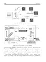
Converter Modes and Synchronization
DDR
PWM
2
w.r.t.
VIN VIN Pin Pin PWMl
DDRi
DDRP
DUAL
Battery VIN HIGH INPHASE
+5V RtoGND HIGH
+90"
ANY
VIN
LOW
+i80"
PRODUCT SPECIFICATION
When used
a$ a
dual
convener
(as
in
Figure
5).
out-of-phase
operation with
180
dcgrce phase shift reduces input current
ripple.
For the '%step" conversion (where the VTl is converted
from VDDQ
as
in Figure 4) used in DDR mode, the duty
cycle
of
the
second
convener
IS
nominally
50%
and the opti-
mal phasing depends
on
VIN. The objective is to keep noise
generated from the switching transition
in one
converter
from influencing the "decision"
to
switch in the other
can-
vener.
When VIN is from the battery, It's typically higher than 7.SV.
As
shown in Figure
6,
180"
"periltion is undesirable
since
the turn-on of the VDDQ convener
occurs
very
near
the
decision point of the VTT converter.
VDDQ
Figure
6.
Noise-susceptible
180'
phasing
for
DDR1
In-phase operation is optimal to reduce inter-converter inter-
ference
when VIN is higher than 5V, (when VIN is from a
battery), as
can
he \een in Figure 7. Since the duty cycle
of PWMl (generating VDDQ) is short, it's switching paint
occurs
far away from the decision point for the VTT
regulator, whose duty cycle
is
nominally
50%.
VDDO
vTT
-
Figure
7.
Optimal In-Phase operation
for
ODR1
When VIN
=
5V,
180"
phase shifted operation
can
be
rejected for the same
reason?
demonstrated Figure
6.
In-phase operation with VIN
=
5V
IS
even
worse, since
the
switch point of either convener occurs
near
the switch point
of the
other
convener
as
seen
in Figure
8.
In
this case, as
VIN
IS
a
little higher than 5V it will tend to
CBUSC
early
termination of the VTT
pulse
width. Conversely, VTTs
switch point can cause early termination of the VDDQ pulse
width when VIN is slightly
lower
than 5V.
REV
1
1
9
5/25/05
9
Appendix
F
Fairchild Specifications for FAN5236
329
PRODUCT
SPECIFICATION
FANS236
Figure
8.
Noise-susceptible In-Phase operation for
DDRP
These problems are nicely solved by delaying the
Znd
con-
verter's clack by 90" as shown in Figure 9.
In
this way,
all
switching transitions
in
one converter
take place far away
from the decision paints of the other converter.
Figure
9.
Optimal
90"
phasing for
DDRP
Initialization and
Soft
Start
Aswming EN
IS
high, FAN5236 is initialized when
VCC
exceeds the rising
UVLO
threshold. Should
VCC
drop
below the
UVLO
threshold,
an
internal Power-On Reset
function disables the chip.
The voltage at the positive input of the error amplifier
is
lim-
ited by the voltage at the
SS
pin which is charged with
a
SpA
current
source.
Once
Css
has charged to VREF (0.9V) the
output voltage will be
~n
regulation. The time it takes
SS
to
reach 0.9V is.
When SS reaches
1
SV,
the Power Goad outputs
are
enabled
and hysteretic mode is allowed. The
converter
is forced into
PWM mode dunng soft start.
Operation
Mode
Control
The made-control circuit changes the converter's mode of
operation from PWM to Hysteretic and visa
versa,
based an
the voltage polarity of the SW node when the lower MOS-
FET is conducting and just before the upper MOSFET turns
on.
For continuous inductor current,
the
SW node
is
negatlve
when
the
lower MOSFET
is
conducting and the converters
operate in fixed-frequency PWM mode
as
shown in Figure
10
This mode of operation achieves high efficiency at nomi-
nal
load. When the load current decreases to
the
paint where
the inductor current flaws through the lower MOSFET
in
the
'reverse' direction,
the
SW node becomes positive, and the
mode
is
changed to hysteretic, which achieves higher eff-
ciency at law currents by decreasing the effective switching
frequency.
To prevent accidental mode change
or
"mode chatter" the
transition from PWM to Hysteretic mode occurs when the
SW node
is
positive for eight consecutive clock cycles
(see
Figure 10) The polarity of
the
SW node is sampled at the
end of
the
lower
MOSFET's conduction time. At the transi-
tion between PWM and hysteretic mode both the upper and
lower MOSFETs are turned
off.
The phase node will
'ring'
based
on
the output inductor and the parasitic capacitance
on
the phase node and settle out at the
value
of the output volt-
age.
The
boundary
value
of
inductor current, where current
becomes discontinuous,
can
be estimated by the following
expression.
where To
9
is
in
Feconds if
Css
is
in
pF.
Figure
10.
Transitioning between PWM
and
Hysteretic Mode
10
REV.
1.1.9
5/25/05
330
Appendix
F
Fairchild Specifications for FAN5236
FAN5236 PRODUCT SPECIFICATION
Hysteretic Mode
Conversely, the transition from Hysteretic mode to PWM
made occurs when the SW node is negative for
8
consecutive
cycles.
A
sudden
increase
in the output current will
also
cause
a
change from hysteretic
to
PWM mode. This load increase
causes
an
instantaneous decrease in the output voltage due to
the voltage drop
on
the
output capacitor ESR. If the load
ciuses the output voltage (as presented at VSNS) to drop
below the hysteretic regulation
level
(20mV below VREF),
the mode is changed to PWM an
the
next clock cycle.
In
hysteretic made,
the
PWM comparator and the
error
amplifier that provide control in PWM mode
are
inhibited
and the hysteretic comparator is activated.
In
hysteretic
mode the
low
side MOSFET is operated as a synchronous
rectifier, where the voltage
across
(
VDs(oN)
)
it is mani-
tored, and it is switched
off
when VDS(ONj goes positive
(current flawing back from the load) allowing the diode to
block
reverse
conduction.
The hysteretic comparator initiates
a
PFM signal to turn
on
HDRV at the rising edge
of
the
next
oscillator clack, when
the output voltage (at VSNS)
falls
below the lower threshold
(10rnV below VREF)
and
terminates the PFM signal when
VSNS rises
over
the higher threshold (SmV above VREF).
The switching frequency is primarily
a
function
of
I
Spread between the two hysteretic thresholds
2.
LOAD
3.
A
transition back to PWM (Continuous Conduction Made
or
CCM) mode
occurs
when the inductor current rises
SUE-
ciently to stay positive far
8
consecutive
cycles.
This
occurs
when.
Output Inductor and Capacitor ESR
where AVHYsTERESIS
=
1SmV and ESR is the equivalent
series
resistance of COu7
Because
of
the different control mechanisms, the
value
of the
load current where transition into CCM operation takes place
is typically higher compared to the load
level
at which transi-
tion into hysteretic mode
occurs.
Hysteretic mode
can
be
disabled by setting the
FPWM
pin low.
.
.
. . . .
. . . .
. . . . . .
S/H
7
Figure
11.
Current Limit/ Summing Circuits
REV.
1.1.9
5/25/05
11
Appendix
F
Fairchild Specifications for
FAN5236
331
PRODUCT SPECIFICATION FAN5236
Current Processing
Section
The following discussion refers
to
Figure
11.
The current through
RSENSE
resistor
(ISNS)
is sampled
shortly after
Q2
is turned
on.
That current is held, and
summed with the output of the error amplifier. This effec-
tively creates
B
current mode control loop. The resistor con-
nected to
ISNSx
pm
(RsENsE)
sets the gain in the current
feedback
loop.
For stable operation, the voltage induced by
the current feedback at the PWM comparator input should
be
set to
30%
of the ramp amplitude at maximum load cument
and line voltage The following expression estimates the
recommended
value
of
RSENSE
as
a
function
of
the maxi-
mum load current
(ILOAD(MAXj)
and the
value
of the
MOSFET’s
RDS(ONj:
ILO*DM*X
.RDSON
.4-IK_IW
(4a)
%“E
=
0.3;.
o.:,,.
v:,,:,,,)
RSENSE
must, however, be kept higher than:
llOAD(MAX)*RDSiON)~
100
(4b)
RSENSECMIN)
=
Setting the Current Limit
A
ratio
of
ISNS
is
also
compared to the current established
when
a
0
9
V
internal reference drives ihe
ILIM
pin:
Since
the tolerance
on
the current limit is largely dependent
on
the ratio of the external resistors it is fairly accurate if the
voltage drop
on
the Switching Node side of
RSENSE
is an
BCCUIBI~
representation of the load current. When using the
MOSFET
as
the sensing element, the variation of
RDS(ON)
causes
proportional variation in the
ISNS.
This
value
not
only
varies
from device
to
device, but
also
hns
a
typical
junc-
tion temperature coefficient of about
0.4%
/
“C
(consult the
MOSFET datasheet
far
actual
values),
so
the
actual
current
limit set point
will
decrease propotiondl to increasing
MOSFET die temperature A factor of
I
.6
in
the current
limit setpomt should compensate
for
all
MOSFET
RosCONj
wnationb, assuming the MOSFET’s heat sinking will keep
its operating die temperature below
125°C.
4
Figure
12.
Improving current sensing accuracy
Mare
accurate sensing can be achieved by
using
a
resistor
(RI)
instead of the
RDS(ONl
of the FET
as
shown in Figure
I2
This approach causes higher
losses,
but yields greater
accuracy
in
both
VDROOP
and
ILIMIr.
RI
is
a
low
value
(e.g. iOmQ) resistor.
Current limit
(ILlMIr)
should be set sufficiently high
as
to
allow
inductor current to
rise
in
response
to
an
output load
transient. Typically,
a
factor
of
1.2
is sufficient.
In
addition,
since
ILIMIT
is
a
peak current cut-off
value,
we will need to
multiply
ILOAD,MAX)
by the inductor
npple
current
(we’ll
use
25%).
For example, in Figure
5
the target for
ILIMlr
would be.
r,,,,,>l2x1.25xL6r6AYl4A
(6)
Duty Cycle Clamp
During
severe load increase, the error amplifier output
can
go to 11s upper limit pushing
a
duty cycle to almost
100%
for
significant amount of time. This could
cause
a large increase
of the mductorcurrent and lead to a long recovery from
a
transient. over-current condition, or even
to
a failure
espe-
cially at high input voltages. To
prevent
this, the output of
the error amplifier
IS
clamped
to
a
fixed
value
after two clock
cycles if severe output voltage exunion is detected, limiting
the maximum duty cycle
to
This circuit is designed to not interfere with normal PWM
operation When FPWM is grounded, the duty cycle
clamp
is disabled and
the
maximum duty cycle is
81%
Gate Driver section
The
Adaptive gate
CO~VOI
logic translates the internal PWM
control
signal into the MOSFET gate drive signals providing
necessary amplification,
level
shifting and shoot-through
protection. Also, it has functions that help optimize the
IC
performance
over
a
wide range of operating conditions.
Since MOSFET switching time can vary dramatically from
type to type and with the input voltage, the gate
cmuol
logic
provides adaptive dead time by monitoring the gate-to-
source
voltages of both
upper
and
lower
MOSFETs.
The
lower
MOSFET
drive
is not turned
on
until
the gate-lo-
source
voltage of ihe
upper
MOSFET has decreased to
less
than approximately
1
volt.
Similarly, the
upper
MOSFET is
not turned
on
until the gate-to-source voltage of the lower
MOSFET has decreased
to less
than approximately
I
volt.
This
allows
a
wide variety of
upper
and
lower
MOSFETs to
be used without
a
concern
for simultaneous conduction,
or
shoot-through.
There must be
a
low-rebistance, low-inductance path
between the driver
pin
and the MOSFET gate
for
the adap-
tive dead-time circuit to work properly. Any delay along that
path
will
subtract from the delay generated by the adaptive
dead-time circit and shoot-through mdy occur.
REV.
1.1.9
5/25/05
12