Fundamentals of Global Positioning System Receivers A Software Approach - Chapter 6 pps
Bạn đang xem bản rút gọn của tài liệu. Xem và tải ngay bản đầy đủ của tài liệu tại đây (222.35 KB, 24 trang )
Fundamentals of Global Positioning System Receivers: A Software Approach
James Bao-Yen Tsui
Copyright
2000 John Wiley & Sons, Inc.
Print ISBN
0-471-38154-3 Electronic ISBN 0-471-20054-9
109
CHAPTER SIX
Receiver Hardware
Considerations
6.1 INTRODUCTION
(1)
This chapter discusses the hardware of the receiver. Since the basic design of
GPS receiver in this book is software oriented, the hardware presented here
is rather simple. The only information needed for a software receiver is the
sampled data. These sampled or digitized data will be stored in memory to
be processed. For postprocessing the memory size dictates the length of data
record. A minimum of
30 seconds of data is needed to find the user position
as mentioned in Section
5.5. In real-time processing the memory serves as a
buffer between the hardware and the software signal processing. The hardware
includes the radio frequency (RF) chain and analog-to-digital converter (ADC).
Thus, the signal processing software must be capable of processing the digitized
data in the memory at a real-time rate. Under this condition, the size of the
memory determines the latency allowable for the signal processing software.
This chapter will include the discussion of the antenna, the RF chain, and the
digitizers. Two types of designs will be discussed. One is a single channel to
collect real data and the other is an in-phase and quadrature phase (I-Q) chan-
nel to collect complex data. In both approaches, the input signals can be either
down-converted to a lower intermediate frequency (IF) before digitization or
directly digitized at the transmitted frequency. The relation between the sam-
pling frequency and the input frequency will be presented. Some suggestions
on the sampling frequency selection will be included. Two hardware setups to
collect real data will be discussed in detail as examples. The impact of the
number of digitized bits will also be discussed.
A digital band folding technique will be discussed that can alias two or more
narrow frequency bands into the baseband. This technique can be used to alias
the L
1 and L2 bands of the GPS into the baseband, or to alias the GPS L1
110 RECEIVER HARDWARE CONSIDERATIONS
frequency and the Russian Global Navigation Satellite System (GLONASS)
signals into the baseband. If one desires, all three bands, L
1, L2, and the
GLONASS, can be aliased into the baseband. With this arrangement the digi-
tized signal will contain the information from all three input bands.
One of the advantages of a software receiver is that the receiver can pro-
cess data collected with various hardware. For example, the data can be real or
complex with various sampling frequencies. A simple program modification in
the receiver should be able to use the data. Or the data can be changed from
real to complex and complex to real such that the receiver can process them.
6.2 ANTENNA
(2–4)
A GPS antenna should cover a wide spatial angle to receive the maximum num-
ber of signals. The common requirement is to receive signals from all satellites
about
5 degrees above the horizon. Combining satellites at low elevation angles
and high elevation angles can produce a low value of geometric dilution of pre-
cision (GDOP) as discussed in Section
2.15. A jamming or interfering signal
usually comes from a low elevation angle. In order to minimize the interfer-
ence, sometimes an antenna will have a relatively narrow spatial angle to avoid
signals from a low elevation angle. Therefore, in selecting a GPS antenna a
trade-off between the maximum number of receiving satellites and interference
must be carefully evaluated.
If an antenna has small gain variation from zenith to azimuth, the strength
of the received signals will not separate far apart. In a code division multiple
access (CDMA) system it is desirable to have comparable signal strength from
all the received signals. Otherwise, the strong signals may interfere with the
weak ones and make them difficult to detect. Therefore, the antenna should
have uniform gain over a very wide spatial angle.
If an antenna is used to receive both the L
1 (1575.42 MHz) and the L2
(1227.6 MHz), the antenna can either have a wide bandwidth to cover the
entire frequency range or have two narrow bands covering the desired frequency
ranges. An antenna with two narrow bands can avoid interference from the sig-
nals in between the two bands.
The antenna should also reject or minimize multipath effect. Multipath effect
is the GPS signal reflections from some objects that reach the antenna indi-
rectly. Multipath can cause error in the user position calculation. The reflection
of a right-handed circular polarized signal is a left-handed polarized signal. A
right-handed polarized receiving antenna has higher gain for the signals from
the satellites. It has a lower gain for the reflected signals because the polariza-
tion is in the opposite direction. In general it is difficult to suppress the mul-
tipath because it can come from any direction. If the direction of the reflected
signal is known, the antenna can be designed to suppress it. One common mul-
tipath is the reflection from the ground below the antenna. This multipath can
be reduced because the direction of the incoming signal is known. Therefore, a
6.3 AMPLIFICATION CONSIDERATION 111
GPS antenna should have a low back lobe. Some techniques such as a specially
designed ground plane can be used to minimize the multipath from the ground
below. The multipath requirement usually complicates the antenna design and
increases its size.
Since the GPS receivers are getting smaller as a result of the advance of inte-
grated circuit technology, it is desirable to have a small antenna. If an antenna
is used for airborne applications, its profile is very important because it will be
installed on the surface of an aircraft. One common antenna design to receive a
circular polarized signal is a spiral antenna, which inherently has a wide band-
width. Another type of popular design is a microstrip antenna, sometimes also
referred to as the patch antenna. If the shape is properly designed and the feed
point properly selected, a patch antenna can produce a circular polarized wave.
The advantage of the patch antenna is its simplicity and small size.
In some commercial GPS receivers the antenna is an integral part of the
receiver unit. Other antennas are integrated with an amplifier. These antennas
can be connected to the receiver through a long cable because the amplifier
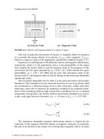
gain can compensate the cable loss. A patch antenna (M
/
A COM ANP-C-114-
5) with an integrated amplifier is used in the data collection system discussed
in this chapter. The internal amplifier has a gain of
26 dB with a noise figure of
2.5 dB. The overall size of the antenna including the amplifier is diameter of
3
′′
and thickness about 0.75
′′
. The antenna pattern is measured in an anechoic
chamber and the result is shown in Figure
6.1a. Figure 6.1b shows the frequency
response of the antenna. The beam of this antenna is rather broad. The gain in
the zenith direction is about +
3.5 dBic where ic stands for isotropic circular
polarization. The gain at
10 degrees is about 3 dBic.
6.3 AMPLIFICATION CONSIDERATION
(5–7,10)
In this section the signal level and the required amplification will be discussed.
The C
/
A code signal level at the receiver set should be at least 130 dBm
(5)
as discussed in Section 5.2. The available thermal noise power N
i
at the input
of a receiver is:
(6)
N
i
kTB watts (6.1)
where k is the Boltzmann’s constant (
1.38 × 10
23
J
/
K) T is the tempera-
ture of resistor R (R is not included in the above equation) in Kelvin, B is the
bandwidth of the receiver in hertz, N
i
is the noise power in watts. The thermal
noise at room temperature where T
290 K expressed in dBm is
N
i
(dBm) 174 dBm
/
Hz or N
i
(dBm) 114 dBm
/
MHz (6.2)
If the input to the receiver is an antenna pointing at the sky, the thermal noise
is lower than room temperature, such as
50 K.
For the C
/
A code signal, the null-to-null bandwidth is about 2 (or 2.046)
112 RECEIVER HARDWARE CONSIDERATIONS
FIGURE 6.1 Antenna measurements of an M/A COM ANP-C-114-5 antenna.
6.3 AMPLIFICATION CONSIDERATION 113
FIGURE 6.1 Continued.
MHz, thus, the noise floor is at 111 dBm ( 114 + 10 log2). Supposing that
the GPS signal is at
130 dBm, the signal is 19 dB ( 130 + 111) below the noise
floor. One cannot expect to see the signal in the collected data. The amplification
needed depends on the analog-to-digital converter (ADC) used to generate the
data. A simple rule is to amplify the signal to the maximum range of the ADC.
However, this approach should not be applied to the GPS signal, because the
signal is below the noise floor. If the signal level is brought to the maximum
range of the ADC, the noise will saturate the ADC. Therefore, in this design the
noise floor rather than the signal level should be raised close to the maximum
range of the ADC.
A personal computer (PC)-based card
(7)
with two ADCs is used to collect
data. This card can operate at a maximum speed of
60 MHz with two 12-bit
ADCs. If both ADCs operate simultaneously, the maximum operating speed is
50 MHz. The maximum voltage to exercise all the levels of the ADC is about
100 mv and the corresponding power is:
P
(0.1)
2
2 × 50
0.0001 watt 0.1 mw 10 dBm (6.3)
114 RECEIVER HARDWARE CONSIDERATIONS
It is assumed that the system has a characteristic impedance of 50 Q . A simple
way to estimate the gain of the amplifier chain is to amplify the noise floor to
this level, thus, a net gain of about
101 dB ( 10 + 111) is needed. Since in
the RF chain there are filters, mixer, and cable loss, the insertion loss of these
components must be compensated with additional gain. The net gain must be
very close to the desired value
(10)
of 101 dB. Too low a gain value will not
activate all the possible levels of the ADC. Too high a gain will saturate some
components or the ADC and create an adverse effect.
6.4 TWO POSSIBLE ARRANGEMENTS OF DIGITIZATION BY
FREQUENCY PLANS
(8,9)
Although many possible arrangements can be used to collect digitized GPS
signal data, there are two basic approaches according to the frequency plan.
One approach is to digitize the input signal at the L
1 frequency directly, which
can be referred to as direct digitization. The other one is to down-convert
the input signal to a lower frequency, called the intermediate frequency (IF),
and digitize it. This approach can be referred to as the down-converted ap-
proach.
The direct digitization approach has a major advantage; that is, in this design
the mixer and local oscillator are not needed. A mixer is a nonlinear device,
although in receiver designs it is often treated as a linear device. A mixer
usually generates spurious (unwanted) frequencies, which can contaminate the
output. A local oscillator can be expensive and any frequency error or impu-
rity produced by the local oscillator will appear in the digitized signal. How-
ever, this arrangement does not eliminate the oscillator (or clock) used for the
ADC.
The major disadvantage of direct digitization is that the amplifiers used in
this approach must operate at high frequency and they can be expensive. The
ADC must have an input bandwidth to accommodate the high input frequency.
In general, ADC operating at high frequency is difficult to build and has fewer
effective bits. The number of effective bits can be considered as the useful
bits, which are fewer than the designed number of bits. Usually, the number
of effective bits decreases at higher input frequency. In this approach the sam-
pling frequency must be very accurate, which will be discussed in Section
6.15.
Another problem is that it is difficult to build a narrow-band filter at a higher
frequency, and usually this kind of filter has relatively high insertion loss.
In the down-converted approach the input frequency is converted to an IF,
which is usually much lower than the input frequency. It is easy to build a
narrow-band filter with low insertion loss and amplifiers at a lower frequency
are less expensive. The mixer and the local oscillator must be used and they
can be expensive and cause frequency errors.
Both approaches will be discussed in the following sections. Some consid-
erations are common to both designs and these will be discussed first.
6.5 FIRST COMPONENT AFTER THE ANTENNA 115
6.5 FIRST COMPONENT AFTER THE ANTENNA
(6)
The first component following the antenna can be either a filter or an ampli-
fier. If the antenna is integrated with an amplifier, the first component after the
antenna is the amplifier. Both arrangements have advantages and disadvantages,
which will be discussed in this section.
The noise figure of a receiver can be expressed as:
(6)
F F
1
+
F
2
1
G
1
+
F
3
1
G
1
G
2
+ ·· · +
F
N
1
G
1
G
2
·· · G
N1
(6.4)
where F
i
and G
i
(i 1, 2, . . . N ) are the noise figure and gain of each individual
component in the RF chain.
If the amplifier is the first component, the noise figure of the receiver is
low and is approximately equal to the noise figure of the first amplifier, which
can be less than
2 dB. The overall noise figure of the receiver caused by the
second component, such as the filter, is reduced by the gain of the amplifier.
The potential problem with this approach is that strong signals in the bandwidth
of the amplifier may drive it into saturation and generate spurious frequencies.
If the first component is a filter, it can stop out-of-band signals from entering
the input of the amplifier. If the filter only passes the C
/
A band, the bandwidth
is around
2 MHz. A filter with 2 MHz bandwidth with a center frequency at
1575.42 MHz is considered high Q. Usually, the insertion loss of such a filter is
relatively high, about
2–3 dB, and the filter is bulky. The receiver noise figure
with the filter as the first component is about
2–3 dB higher than the previous
arrangement. Usually, a GPS receiver without special interfering signals in the
neighborhood uses an amplifier as the first component after the antenna to obtain
a low noise figure.
6.6 SELECTING SAMPLING FREQUENCY AS A FUNCTION OF THE C
/
A
CODE CHIP RATE
An important factor in selecting the sampling frequency is related to the C
/
A
code chip rate. The C
/
A code chip rate is 1.023 MHz and the sampling fre-
quency should not be a multiple number of the chip rate. In other words, the
sampling should not be synchronized with the C
/
A code rate. For example,
using a sampling frequency of
5.115 MHz (1.023 × 5) is not a good choice. With
this sampling rate the time between two adjacent samples is
195.5 ns (1
/
5.115
MHz). This time resolution is used to measure the beginning of the C
/
A
code. The corresponding distance resolution is
58.65 m (195.5 × 3 × 10
8
m).
This distance resolution is too coarse to obtain the desired accuracy of the user
position. Finer distance resolution should be obtained from signal processing.
With synchronized sampling frequency, it is difficult to obtain fine distance res-
olution. This phenomenon is illustrated as follows.
Figure
6.2 shows the C
/
A code chip rate and the sampled data points. Fig-
116 RECEIVER HARDWARE CONSIDERATIONS
FIGURE 6.2 Relation between sampling rate and C
/
A code.
ures 6.2a and 6.2b show the synchronized and the unsynchronized sampling,
respectively. In each figure there are two sets of digitizing points. The lower
row is a time-shifted version of the top row.
In Figure
6.2a, the time shift is slightly less than 195.5 ns. These two sets
of digitizing data are exactly the same as shown in this figure. This illustrates
that shifting time by less than
195.5 ns produces the same output data, if the
sampling frequency is synchronized with the C
/
A code. Since the two digitized
data are the same, one cannot detect the time shift. As a result, one cannot
derive finer time resolution (or distance) better than
195.5 ns through signal
processing.
In Figure
6.2b the sampling frequency is lower than 5.115 MHz; therefore, it
is not synchronized with the C
/
A code. The output data from the time-shifted
case are different from the original data as shown in the figure. Under this
condition, a finer time resolution can be obtained through signal processing
to measure the beginning of the C
/
A code. This fine time resolution can be
converted into finer distance resolution.
As discussed in Chapter
3, the Doppler frequency on the C
/
A code is about
±
6 Hz, which includes the speed of a high-speed aircraft. Therefore, the code
frequency should be considered as in the range of
1.023 × 10
6
±6 Hz. The
sampling frequency should not be a multiple of this range of frequencies. In
general, even in the sampling frequency is close to the multiple of this range
of frequencies, the time-shifted data can be the same as the original data for a
period of time. Under this condition, in order to generate a fine time resolution,
a relatively long record of data must be used, which is not desirable.
6.7 SAMPLING FREQUENCY AND BAND ALIASING FOR REAL DATA COLLECTION 117
6.7 SAMPLING FREQUENCY AND BAND ALIASING FOR REAL DATA
COLLECTION
(10)
If only one ADC is used to collect digitized data from one RF channel, the
output data are often referred to as real data (in contrast to complex data). The
input signal bandwidth is limited by the sampling frequency. If the sampling
frequency is f
s
, the unambiguous bandwidth is f
s
/
2. As long as the input signal
bandwidth is less than f
s
/
2, the information will be maintained and the Nyquist
sampling rate will be fulfilled. Although for many low-frequency applications
the input signal can be limited to
0 to f
s
/
2, in general, the sampling frequency
need not be twice the highest input frequency.
If the input frequency is f
i
, and the sampling frequency is f
s
, the input fre-
quency is aliased into the baseband and the output frequency f
o
is
f
o
f
i
nf
s
/
2 and f
o
< f
s
/
2 (6.5)
where n is an integer. The relationship between the input and the output fre-
quency is shown in Figure
6.3.
When the input is from nf
s
to (2n + 1)f
s
/
2, the frequency is aliased into
the baseband in a direct transition mode, which means a lower input frequency
translates into a lower output frequency. When the input is from (
2n + 1)f
s
/
2
to (n + 1)f
s
, it is aliased into the baseband in an inverse transition mode, which
means a lower input frequency translates into a higher output frequency. Either
case can be implemented if the frequency translation is properly monitored.
If the input signal bandwidth is Df , it is desirable to have the minimum
sampling frequency f
s
higher than the Nyquist requirement of 2Df . Usually,
2.5Df is used because it is impractical to build a filter with very sharp skirt (or
a brick wall filter) to limit the out-of-band signals. Thus, for the C
/
A code the
required minimum sampling rate is about
5 MHz. This sampling frequency is
adequately separated from the undesirable frequency of
5.115 MHz. The sam-
pling frequency must be properly selected. Figure
6.4a shows the desired fre-
quency aliasing. The input band is placed approximately at the center of the
FIGURE 6.3 Input versus output frequency of band aliasing.
118 RECEIVER HARDWARE CONSIDERATIONS
FIGURE 6.4 Frequency aliasing for real data collection.
output band and the input and output bandwidths are equal.
Figure
6.4b shows improper frequency aliasing. In Figure 6.4b, the center
frequency of the input signal does not alias to the center of the baseband. The
frequency higher than (
2n + 1)f
s
/
2 and the portion of the frequency lower than
(
2n + 1)f
s
/
2 are aliased on top of each other. Therefore, portion of the output
band contains an overlapping spectrum, which is undesirable. When there is a
spectrum overlapping in the output, the output bandwidth is narrower than the
input bandwidth.
In order to alias the input frequency near the center of the baseband, the
following relation must hold,
f
o
f
i
n( f
s
/
2) ≈ f
s
/
4 and f
s
> 2Df (6.6)
where Df is the bandwidth of input signal. The first part of this equation is to put
the aliasing signal approximately at the center of the output band. The second
part states that the Nyquist sampling requirement must hold. If the frequency
of the input signal f
i
is known, this equation can be used to find the sampling
frequency. Examples will be presented in Sections
6.8 and 6.9.
6.8 DOWN-CONVERTED RF FRONT END FOR REAL DATA COLLECTION 119
6.8 DOWN-CONVERTED RF FRONT END FOR REAL DATA
COLLECTION
(8–10)
In this section a down-converted approach to digitize the signal will be dis-
cussed. The IF and sampling frequency will be determined, followed by some
general discussion. A set of hardware to collect data for user location calcula-
tion will be presented.
In this approach the input signal is down converted to an IF, then digitized
by an ADC. In Equation (
6.6) there are three unknowns: n, f
i
, and f
s
; therefore,
the solutions are not unique. Many possible solutions can be selected to build
a receiver. In the hardware design, the sampling frequency of f
s
5 MHz is
selected. From Equation (
6.6) f
i
IF 5n + 1.25 MHz, where n is an integer.
The value of n
4 is arbitrarily selected and the corresponding IF 21.25 MHz,
which can be digitized by an ADC.
Of course, one can choose n
0 and down convert the input frequency to 1.25
MHz directly. In this approach the mixer generates more spurious frequencies.
The input signal is down-converted to from
0.25 to 2.25 MHz, which covers
more than an octave bandwidth. An octave bandwidth means that the highest
frequency in the band is equal to twice the lowest frequency in the band. A
common practice in receiver design is to keep the IF bandwidth under an octave
to avoid generation of in-band second harmonics.
There are many different ways to build an RF front end. The two important
factors are the total gain and filter installations. Filters can be used to reject
out-of-band signals and limit the noise bandwidth, but they add insertion loss.
If multiple channels are used, such as in the I-Q channels, filters may increase
the difficulty of amplitude and phase balancing. The locations of filters in a
receiver affect the performance of the RF front end.
The personal computer–based ADC card discussed in Section
6.3 is used as
the ADC. It requires about
100 mv input voltage or 10 dBm to activate all the
bits. A net gain of
101 dB is required to achieve this level. If a digital scope
is used as the ADC
(8,9)
because of the built-in amplifiers in the scope, it can
digitize a rather weak signal. In this kind of arrangement, only about
90 dB
gain is used.
Two RF front-end arrangements are shown in Figure
6.5. The major differ-
ence between Figures
6.5a and b is in the amplifiers. In Figure 6.5a amplifiers
2, 3, and 4 operate at IF, which costs less than amplifiers operating at RF. Fil-
ter
1 is used to limit the input bandwidth. Filter 2 is used to limit the spurious
frequencies generated by the mixer, and filter
3 is used to limit noise gener-
ated by the three amplifiers. Although Figure
6.5a is the preferred approach, in
actual laboratory experiments Figure
6.5b is used because of the availability of
amplifiers.
In Figure
6.5b, the M
/
A COM ANP-C-114-5 antenna with amplifier is used.
Amplifier
1 is an integrated part of the antenna with a 26 dB gain and a 2.5
dB noise figure. The bias T is used to supply 5-volt dc to the amplifier at the
antenna. Filter
1 is centered at 1575.42 MHz with a 3 dB bandwidth of 3.4 MHz,
120 RECEIVER HARDWARE CONSIDERATIONS
FIGURE 6.5 Two arrangements of data collection.
which is wider than the desired value of 2 MHz. Amplifiers 2 and 3 provide a
total of
60 dB gain. The frequency of the local oscillator is at 1554.17 MHz.
The mixer-down converts the input frequency from
1575.42 to 21.25 MHz.
In this frequency conversion, high input frequency transforms to high output
frequency. The attenuator placed between the mixer and the oscillator is used to
improve impedance matching and it reduces the power to the mixer. After the
mixer an IF amplifier with
24 dB of gain is used to further amplify the signal.
Finally, filter
2 is used to reject spurious frequencies generated by the mixer
and limit the noise bandwidth. Filter
2 has a center frequency of 21.25 MHz
and bandwidth of
2 MHz. If filter 2 is not used all the noise will alias into the
output band and be digitized by the ADC as shown in Figure
6.3. The overall
gain from the four amplifiers is
110 dB (26 + 30 + 30 + 24). Subtracting the
insertion losses from the filters, bias T, and mixer, the gain is slightly over
100
dB. There is no filter after the mixer because it is not available.
6.9 DIRECT DIGITIZATION FOR REAL DATA COLLECTION 121
6.9 DIRECT DIGITIZATION FOR REAL DATA COLLECTION
(8,9)
Direct digitization at RF is a straightforward approach. The only components
required are amplifiers and two filters. The amplifiers must provide the desired
RF gain. One filter is used after the first amplifier to limit out-of-band signal
and the second filter is placed in front of the ADC to limit the noise bandwidth.
A direct digitization arrangement is shown in Figure
6.6. In this arrangement
the second filter is very important. Without this filter the noise in the collected
data can be very high and it will affect signal detection.
In the direct sampling case, the frequency of the input signal is fixed; one
must find the correct sampling frequency f
s
to avoid band overlapping in the
output. In this approach there are two unknowns: f
s
and n, in Equation (6.6).
An exact solution is somewhat difficult to obtain. However, the problem can
be easily solved if the approximate sampling frequency is known.
Let us use an example to illustrate the operation. In this example, the input
GPS L
1 signal is at 1575.42 MHz, and the sampling frequency is about 5 MHz.
First use Equation (
6.5) with f
o
1.25 MHz, f
i
1575.42 MHz, and f
s
5 MHz to find n 629.66. Round off n 630 and use f
o
f
s
/
4 in Equation
(
6.6). The result is f
s
5.009 MHz and the center is aliased to 1.252 MHz.
In one arrangement a scope is used to collect digitized data because the
personal computer–based ADC card cannot accommodate the frequency of the
input signal. The scope has a specified bandwidth of dc-
1000 MHz, but it can
digitize a signal at
1600 MHz with less sensitivity. The scope can operate at
5 MHz, but the sampling frequency cannot be fine-tuned. If 5 MHz is used to
sample the input frequency, the center frequency will be aliased to
420 KHz.
Since the bandwidth of the C
/
A code is 2 MHz, there is band overlapping with
the center frequency at
420 KHz as shown in Figure 6.7.
Actual GPS data were collected through this arrangement. Although there
is band overlapping, the data could still be processed, because the overlapping
range is close to the edge of the signal where the spectrum density is low. In
this arrangement, the overall amplification is reduced because the scope can
digitize weak signals.
In another arrangement, an experimental ADC built by TRW is used. The
ADC can sample only between approximately
80 to 120 MHz, limited by the
circuit around the ADC. In order to obtain digitized data at
5 MHz, the output
FIGURE 6.6 Arrangement for Direct Digitization.
122 RECEIVER HARDWARE CONSIDERATIONS
FIGURE 6.7 Band aliasing for direct sampling of the L1 frequency at 5 MHz.
from the ADC is decimated. For example, if the ADC operates at 100 MHz
and one data point is kept out of every
20 data points, the equivalent sampling
rate is
5 MHz. The actual sampling frequency is selected to be 5.161 MHz; the
input signal is aliased to
1.315 MHz, which is close to the center of the output
band at about
1.29 (5.161
/
4) MHz.
With today’s technology, it is easier to build a down-converted approach, but
the direct digitization is attractive for its simplicity. There is another advantage
for direct digitization, which is to alias more than one desired signal into the
baseband. This approach will be discussed in Section
6.11.
6.10 IN-PHASE (I) AND QUADRANT-PHASE (Q) DOWN
CONVERSION
(10)
In many commercial GPS receivers, the input signal is down converted into
I-Q channels. The data collected through this approach are complex and the
two sets of data are often referred to as real and imaginary. Since there are two
channels, the Nyquist sampling is f
s
Df . A common practice is to choose
f
s
> 1.25Df to accommodate the skirt of the filter. The relation between the
input and the output frequencies is
f
o
f
i
nf
s
and f
o
< f
s
(6.7)
where n is a positive integer. The relation between the input and output band
is shown in Figure
6.8. In the I-Q channel digitization, as long as Df < f
s
there
is no spectrum overlapping in the output baseband.
6.11 ALIASING TWO OR MORE INPUT BANDS INTO A BASEBAND 123
FIGURE 6.8 Frequency aliasing for complex data collection.
A common frequency selection is shown in Figure 6.8. The center of the
output frequency is placed at zero. This approach usually can be achieved only
through a down-converted design, and the input frequency f
i
is usually set to
zero or to a multiple of the sampling frequency f
s
. In this arrangement, the
input frequency is divided into two equal bands. The lower input frequency is
aliased to a higher frequency in the baseband and the higher input frequency is
aliased to a lower frequency as shown in Figure
6.8. This phenomenon affects
the data conversion procedure discussed in Section
6.14.
There are two ways to build an I-Q down converter as shown in Figure
6.9.
In Figure
6.9a, a 90-degree phase shift is introduced in the input circuit. In Fig-
ure
6.9b, the 90-degree phase shift is introduced in the oscillator circuit. Both
approaches are popularly used. If one wants the output frequency to be zero, the
local oscillator is often selected as the input signal or at
1575.42 MHz. For a wide-
band receiver the I-Q approach can double the input bandwidth with the same
sampling frequency. Since the GPS receiver bandwidth is relatively narrow, this
approach is not needed to improve the bandwidth. This approach uses more hard-
ware because one additional channel is required. The amplitude and phase of the
two outputs are difficult to balance accurately. From the software receiver point
of view, there is no obvious advantage of using an I-Q channel down converter.
Actual complex data with zero center frequency have been collected. Since
the acquisition and tracking programs used in this book can process only real
data, the complex data are converted into real data through software. The details
will be presented in Section
6.14.
6.11 ALIASING TWO OR MORE INPUT BANDS INTO A BASEBAND
(8,9)
If one desires to receive signals from two separate bands, the straightforward
way is to use two mixers and two local oscillators to covert the two input bands
124 RECEIVER HARDWARE CONSIDERATIONS
FIGURE 6.9 I and Q down converter.
into desired IF ranges such as adjacent bands, combine, and digitize them. if
direct digitization is used and the correct sampling frequency is selected, two
input bands can be aliased into a desired output band. Figure
6.10 shows the
arrangement of aliasing two input bands into the baseband for a real data col-
lection system.
The aliased signals in the baseband can be either overlapped or separated.
In Figure
6.10 the two signals in the baseband are separated. Separated bands
have better signal-to-noise ratio because the noise in the two bands is separated.
Separated spectra occupy a wider frequency range and require a higher sampling
rate. The overlapped bands have lower signal-to-noise ratio because the noise of
two bands is added together. Overlapped spectra occupy a narrower bandwidth
and require a lower sampling rate. The aliasing scheme can be used to fold more
than two input bands together and it also applies to complex data collection.
Before the input bands can be folded together, analog filters must be used to
properly filter the desired input bands.
FIGURE 6.10 Aliasing two input bands to baseband.
6.11 ALIASING TWO OR MORE INPUT BANDS INTO A BASEBAND 125
FIGURE 6.11 Aliasing of L1 and L2 bands to baseband.
Let us use three examples to illustrate the band aliasing idea. In the first
example the two P code channels from both L
1 and L2 frequencies are aliased
into two separated bands in the baseband. Since the P code has a bandwidth of
approximately
20 MHz, two P code bands will occupy 40 MHz. The minimum
sampling frequency to cover these bands is about
100 MHz (40 × 2.5), if 2.5
rather than the Nyquist sampling rate of 2 is used as the minimum required
sampling rate. The two input frequency ranges are
1565.42–1585.42 MHz and
1217.6–1237.6 MHz for L1 and L2 bands, respectively. It is tedious to solve
the desired sampling frequency. It is easier to solve the sampling frequency
f
s
through trial and error. The output frequency can be obtained from Equa-
tion (
6.5) by increasing the sampling frequency in 100 KHz steps starting from
100 MHz. When the two output frequency ranges are properly aliased into the
baseband, the sampling frequency is the desired one. There are many sampling
frequencies that can fulfill this requirement. One of the lower sampling fre-
quencies is arbitrarily selected, such as f
s
107.8 MHz. With this sampling
frequency, the L
1 band is aliased to 2.32–22.32 MHz, and the L2 band is aliased
to
31.8–51.8 MHz. These two bands are not overlapped and they are within the
baseband of
0–53.9 (f
s
/
2) MHz. Figure 6.11 shows such an arrangement.
In the second example, the same two bands are allowed to partially overlap
after they are aliased into the baseband. The sampling frequency can be found
through the same approach. The output bandwidth can be as narrow as
20 MHz,
when the input bands are totally overlapped. Therefore, the minimum sampling
frequency is about
50 MHz. if the sampling frequency f
s
57.8 MHz, the L1
frequency aliases to 3.8–23.8 MHz and L2 aliases to 4.82–24.82 MHz and they
are partially overlapped. The output bandwidth is from
0 to 28.9 ( f
s
/
2) MHz.
The third example is to alias the C
/
A band of the GPS signal and Russia’s
GLONASS signal into separate bands in the baseband. The GLONASS is Rus-
sia’s standard position system, which is equivalent to the GPS system of the
United States. The GLONASS uses bi-phase coded signals with
24 channels
at frequencies
1602 + 0.5625 n where n is an integer representing the chan-
nel number. A future plan to revise the frequency channels used will eliminate
a number of the upper channels. Therefore, only the
1–12 channels will be
considered. The center frequency of these
12 channels is at 1605.656 (1602 +
126 RECEIVER HARDWARE CONSIDERATIONS
0.5625 × 6.5) MHz. The total bandwidth is 7.3125 (0.5625 × 13) MHz. For sim-
plicity let us use a
7.5 MHz bandwidth, the signal frequency is approximately
1601.9–1609.4 MHz. Including the C
/
A code of the GPS signal, the overall
bandwidth is about
9.5 MHz. The minimum sampling frequency can be 23.75
(9.5 × 2.5) MHz. If f
s
35.1 MHz, the GPS channel is aliased to 12.47–14.47
MHz, the GLONASS to 4.8–12.35 MHz, and both signals are within the 0 to
17.55 ( f
s
/
2) MHz baseband. Hardware has been built to test this idea. The
collected data contain both the GPS and the GLONASS signals.
6.12 QUANTIZATION LEVELS
(11–13)
As discussed in Section 5.3, GPS is a CDMA signal. In order to receive the
maximum of signals, it is desirable to have comparable signal strength from all
visible satellites at the receiver. Under this condition, the dynamic range of a
GPS receiver need not be very high. An ADC with a few bits is relatively easy
to fabricate and may operate at high frequency. Another advantage of using
fewer bits is that it is easier to process the digitized data, especially when they
are processed through hardware. The disadvantage of using fewer bits is the
degradation of the signal-to-noise ratio. Spilker
(11)
indicated that a 1-bit ADC
degrades the signal-to-noise ratio by
1.96 dB and a 2-bit ADC degrades the
signal-to-noise by
0.55 dB. Many commercial GPS receivers use only 1- or
2-bit ADCs.
Chang
(12)
claims that the degradation due to the number of bits of the ADC
is a function of input signal-to-noise ratio and sampling frequency. Low signal-
to-noise ratio signal sampled at a higher frequency causes less degradation in a
receiver. The GPS signal should belong to the low signal-to-noise ratio because
the signal is below the noise. At a Nyquist sampling rate, the minimum degra-
dation is about
3.01 and 0.72 dB for 1- and 2-bit quantizers, respectively. At
five times the Nyquist sampling rate, the minimum degradation is
2.18 and .60
dB for 1- and 2-bit quantizers, respectively. These values are slightly higher
than the results in reference
11.
The only time that a high number of bits in ADC is required in a GPS
receiver is to build a receiver with antijamming capability. Usually, the jam-
ming signal is much stronger than the desired GPS signals. An ADC with a
small number of bits will be easily saturated by the jamming signal. Under this
condition, the GPS signals might be masked by the jamming signal and the
receiver cannot detect the desired signals. If an ADC with a large number of
bits is used, the dynamic range of the receiver is high. Under this condition,
the jamming signal can still disturb the operation; however, the weak GPS sig-
nals are preserved in the digitized data. If proper digital signal processing is
applied, the GPS signals should be recovered. This problem can be considered
in the frequency domain. Assume that there are two signals, a strong one and a
weak one, and they are close in frequency. In order to receive both signals, the
receiver must have enough instantaneous dynamic range, which is defined as
6.13 HILBERT TRANSFORM 127
the capability to receive strong and weak signals simultaneously. If the ADC
does not have enough dynamic range, the weak signal may not be received.
Reference
12 provides more information on this subject.
6.13 HILBERT TRANSFORM
(10)
In this book a single channel is used to collect data and the software is written
to process real data. If a software receiver is designed to process complex data
and only real data are available, the real data can be changed to complex data
through the Hilbert transform.
(10)
A detailed discussion on the Hilbert transform
will not be included. Only the procedure will be presented here.
First the Hilbert transform from Matlab will be presented. The approach is
through discrete Fourier transform (DFT) or fast Fourier transform (FFT). The
following steps are taken:
1. The DFT result can be written as:
X(k)
N 1
∑
n 0
x(n)e
j2pnk
N
(6.8)
where x(n) is the input data, X(k) is the output frequency components, k
0, 1, 2, . . . , N 1, and n 0, 1, 2, . . . , N 1. Since the input data are
real, the frequency components have the following properties:
X(k)
X(N k)
*
for k 1 ∼
N
2
1 (6.9)
where
*
represents complex conjugate. If the input data are complex the
relationship in this equation does not exist.
2. Find a new set of frequency components X
1
(k). They have the following
values:
X
1
(0)
1
2
X(0)
X
1
(k) X(k) for k 1 ∼
N
2
1
X
1
N
2
1
2
X
N
2
X
1
(k) 0 for k
N
2
+ 1 ∼ N 1 (6.10)
128 RECEIVER HARDWARE CONSIDERATIONS
These new frequency components also have N values from k 0 to N 1.
3. The new data x
1
(n) in time domain can be obtained from the inverse DFT
of the X
1
(k) as:
x
1
(n)
1
N
N 1
∑
k 0
X
1
(k)e
j2pnk
N
(6.11)
From this approach, if there are N points of real input data, the result will be N
points of complex data. Obviously, additional information is generated through
this operation. This is caused by padding the X
1
(k) values with zeros as shown
in Equation (
6.10). Padding with zeros in the frequency domain is equivalent
to interpolating in the time domain.
(10)
The above method generates N points of complex data from N points of real
data. The new data may increase the processing load without gaining significant
receiver performance improvement. Therefore, another approach is presented,
which is similar to the above Matlab approach, but generates only N
/
2 points
of complex data. In taking real digitized data the sampling frequency f
s
≈ 2.5
Df is used and the input signal is aliased close to the center of the baseband.
Under this condition, the frequency component X(N
/
2) should be very small.
The following steps can be taken to obtain complex data:
1. The first step is the same as step 1 (Equation 6.8) in the Matlab approach
to take the FFT of the input signal.
2. The new X
1
(k) can be obtained as
X
1
(k) X(k) for k 0, 1, 2, . . . ,
N
2
1 (6.12)
Therefore, only half of the frequency components are kept.
3. The new data in time domain can be obtained as
x
1
(n)
2
N
N
2
1
∑
k 0
X
1
(k)e
j4pnk
N
(6.13)
The final results are N
/
2 points of complex data in the time domain and they
contain the same information as the N points of real data. These data cover the
same length of time; therefore, the equivalent sampling rate of the complex data
is f
s1
f
s
/
2. The argument is reasonable because for complex data the Nyquist
sampling rate is f
s1
Df .
6.14 CHANGE FROM COMPLEX TO REAL DATA 129
6.14 CHANGE FROM COMPLEX TO REAL DATA
In this section changing complex data to real data will be discussed. The
approach basically reverses the operation in Section
6.13. However, the IF of
the down conversion is very important in this operation. The detail operation
depends on this frequency. One of the common I-Q converter designs is to make
the IF at zero frequency as shown in Figure
6.8. Under this condition, the cen-
ter frequency of the input signal is determined by the Doppler shift. For this
arrangement the following steps can be taken:
1. Take the DFT of x(n) to generate X(k) as shown in Equation (6.8),
X(k)
N 1
∑
n 0
x(n)e
j2pnk
N
(6.14)
where x(n) is complex, k
0, 1, 2, . . . , N 1, and n 0, 1, 2, . . . , N 1.
2. Generate a new set of frequency components X
1
(k) from X(k) as
X
1
(k) X
N
2
+ k
for k 0 ∼
N
2
1
X
1
(k) X
N
2
+ k
for k
N
2
∼ N 1 (6.15)
In Figure
6.8, the lower input frequency is converted into a higher output
frequency and the higher frequency is converted into a lower frequency.
This operation puts the two separate bands in Figure
6.8 into the correct
frequency range as the input signals. Or one can consider that it shifts
the center of the input signal from zero to f
s
/
2. If the IF is not at zero
frequency a different shift is required. If the IF of the I-Q channels is at
f
s
/
2, no shift is required and this step can be omitted, because the input
signal will not split into two separate bands.
3. Generate additional frequency components for X
1
(k) as
X
1
(N ) 0
X
1
(N + k) X
1
(N k)
*
for k 1 ∼ N 1 (6.16)
Including the results from Equation (
6.15) there are total 2N frequency
components from k
0 ∼ 2N 1.
4. The final step is to find the new data in the time domain through inverse
FFT as
130 RECEIVER HARDWARE CONSIDERATIONS
x
1
(n)
1
2
N
2N 1
∑
k 0
X
1
(k)e
jpnk
N
(6.17)
The N points of complex data generate
2N points of real data and they
contain the same amount of information. These
2N points cover the same
time period; therefore, the equivalent sampling frequency is doubled or
f
s1
2f
s
.
Actual complex data are collected from satellites with I-Q channels of zero IF
from Xetron Corporation. The sampling frequency is
3.2 MHz and the Nyquist
bandwidth is also
3.2 MHz. The operations from Equations (6.14) to (6.17)
are used to change these data to real data with IF
1.6 MHz. The number of
real data is double the number of complex data and the equivalent sampling
frequency is
6.4 MHz. These data are processed and the user position has been
found.
6.15 EFFECT OF SAMPLING FREQUENCY ACCURACY
Although the sampling frequency discussed in this chapter is given a certain
mathematical value, the actual frequency used in the laboratory usually has
limited accuracy. The effect of this inaccuracy will be discussed as follows.
The first impact to be discussed is on the center frequency of the digitized
signal. For the down-converted approach, the sampling frequency inaccuracy
causes a small error in the output frequency. For example, if the IF is at
21.25
MHz and the sampling frequency is at 5 MHz, the digitized output should be at
1.25 MHz. This value can be found from Equation (6.5) and the corresponding n
4. If the true sampling frequency f
s
5,000,100 Hz, there is an error frequency
of
100 Hz. The center frequency of the digitized signal is at 1,249,600 Hz.
The error frequency is
400 Hz, which is four times the error in the sampling
frequency because in this case n
4. This frequency error will affect the search
range of the acquisition procedure.
For a direct digitization system, the error in the sampling frequency will
create a larger error in the output frequency. As discussed in Section
6.9, if
the sampling frequency f
s
5,161,000 Hz, with the input signal at 1575.42
MHz, the output will be 1.315 MHz with n 305 from Equation (6.5). If f
s
5,161,100 Hz, which is off by 100 Hz from the desired value, the input will be
aliased to
1,284,500 Hz, which is off by 30,500 Hz because n 305. The fre-
quency error will have a severe impact on the acquisition procedure. Therefore,
for the direct digitization approach the accuracy of the sampling frequency is
rather important.
The second impact of inaccurate sampling frequency is on the processing of
the signal. In a software receiver, both the acquisition and tracking programs
6.16 SUMMARY 131
take the sampling frequency as input. If the actual sampling frequency is off
by too much the acquisition program might not cover the anticipated frequency
range and would not find the signal. For a small error in sampling frequency, it
will not have a significant effect on the acquisition and the tracking programs.
For example, the sampling frequency of
3.2 MHz used to collect the complex
data must be off slightly because all the Doppler frequencies calculated are of
one sign. If the correct sampling frequency is used in the program, the Doppler
frequency should have both positive and negative values because the receiving
antenna is stationary. From these experimental results, no obvious adverse effect
on the acquisition and tracking is discovered due to the slight inaccuracy of the
sampling frequency.
The most important effect of sampling frequency inaccuracy may be the
pseudorange measured. The differential pseudorange is measured by sampling
time, which will be discussed in Section
9.9. If the sampling frequency is not
accurate, the sampling time will be off. The inaccuracy in the pseudorange will
affect the accuracy of the user position measured.
6.16 SUMMARY
This chapter discusses the front end of a GPS receiver. The antenna should
have a broad beam to receive signals from the zenith to the horizon. It should
be right handed circularly polarized to reduce reflected signals. The overall gain
of the amplifier chain depends on the input voltage of the ADC. Usually the
overall gain is about
100 dB. The input signal can either be down converted
and then digitized or directly digitized without frequency translation. Although
direct digitization seems to have some advantages, with today’s technology a
down conversion approach is simpler to build. It appears that I-Q channel down
conversion does not have much advantage over a single channel conversion for
a software GPS receiver. Direct digitization can be used to alias several narrow
input signals into the same baseband. Several experimental setups to collect
data are presented. The number of quantization bits is discussed. One or two
bits may be enough for GPS application with degradation of receiver sensitivity.
If antijamming is of concern, a large number of bits needed. The conversion of
data from real to complex and from complex to real are discussed. Finally, the
impact of sampling frequency accuracy is discussed.
REFERENCES
1. Van Dierendonck, A. J., “GPS receivers,” Chapter 8 in Parkinson, B. W., Spilker,
J. J. Jr., Global Positioning System: Theory and Applications, vols.
1 and 2, Ameri-
can Institute of Aeronautics and Astronautics,
370 L’Enfant Promenade, SW, Wash-
ington, DC,
1996.
2. Bahl, I. J., Bhartia, P., Microstrip Antennas, Artech House, Dedham, MA, 1980.
132 RECEIVER HARDWARE CONSIDERATIONS
3. Johnson, R. C., Jasik, H., eds., Antenna Engineering handbook, McGraw-Hill, New
York,
1984.
4. Braasch, M. S., “Multipath effects,” Chapter 14 in Parkinson, B. W., Spilker, J. J.
Jr., Global Positioning System: Theory and Applications, vols.
1 and 2, American
Institute of Aeronautics and Astronautics,
370 L’Enfant Promenade, SW, Washing-
ton, DC,
1996.
5. Spilker, J. J. Jr., “GPS signal structure and theoretical performance,” Chapter 3 in
Parkinson, B. W., Spilker, J. J. Jr., Global Positioning System: Theory and Appli-
cations, vols.
1 and 2, American Institute of Aeronautics and Astronautics, 370
L’Enfant Promenade, SW, Washington, DC, 1996.
6. Tsu, J. B. Y., Microwave Receivers with Electronic Warfare Applications, Wiley,
New York,
1986.
7. GaGe Scope Technical Reference and User’s Guide, GaGe Applied Sciences, 5610
Bois Franc, Montreal, Quebec, Canada.
8. Tsui, J. B. Y., Akos, D. M., “Comparison of direct and downconverted digitization
in GPS receiver front end designs,” IEEE MTT-S International Microwave Sympo-
sium, pp.
1343–1346, San Francisco, CA, June 17–21, 1996.
9. Akos, D. M., Tsui, J. B. Y., “Design and implementation of a direct digitization
GPS receiver front end,” IEEE Trans. Microwave Theory and Techniques, vol.
44,
no.
12, pp. 2334–2339, December 1996.
10. Tsui, J. B. Y., Digital Techniques for Wideband Receivers, Artech House, Boston,
1995.
11. Spilker, J. J. Jr., Digital Communication by Satellite, pp. 550–555, Prentice Hall,
Englewood Cliffs, NJ,
1995.
12. Chang, H., “Presampling filtering, sampling and quantization effects on the digital
matched filter performance,” Proceedings of International Telemetering Conference,
pp.
889–915, San Diego, CA, September 28–30, 1982.
13. Moulin, D., Solomon, M. N., Hopkinson, T. M., Capozza, P. T., Psilos, J., “High
performance RF-to-digital translators for GPS anti-jam applications,” ION GPS-
98,
pp.
233–239, Nashville, TN, September 15–18, 1998.