rfid handbook fundamentals and applications in contactless smart cards and identification second edition phần 7 pptx
Bạn đang xem bản rút gọn của tài liệu. Xem và tải ngay bản đầy đủ của tài liệu tại đây (2.93 MB, 52 trang )
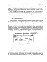
Table 11.1: Example of the execution of a read command by the application
software, reader and transponder
Application ↔ readerReader ↔
transponder
Comment
→
Blockread_Address[00]
Read transponder
memory [address]
→ Request
Transponder in
the field?
←
ATR_SNR[4712]
Transponder
operates with
serial number
→ GET_ Random
Initiate
authentication
←
Random[081514]
→ SEND_Token1
← GET_Token2
Authentication
successfully
completed
→ Read_@[00]
Read command
[address]
←
Data[9876543210]
Data from
transponder
← Data[9876543210]
Data to application
The reader's main functions are therefore to activate the data carrier
(transponder), structure the communication sequence with the data carrier, and
transfer data between the application software and a contactless data carrier.
All features of the contactless communication, i.e. making the connection, and
performing anticollision and authentication procedures, are handled entirely by
the reader.
This document was created by an unregistered ChmMagic, please go to to register it. Thanks.
11.2 Components of a Reader
A number of contactless transmission procedures have already been described in the
preceding chapters. Despite the fundamental differences in the type of coupling
(inductive — electromagnetic), the communication sequence (FDX, HDX, SEQ), the
data transmission procedure from the transponder to the reader (load modulation,
backscatter, subharmonic) and, last but not least, the frequency range, all readers are
similar in their basic operating principle and thus in their design.
Readers in all systems can be reduced to two fundamental functional blocks: the
control system and the HF interface, consisting of a transmitter and receiver (Figure
11.2). Figure 11.3 shows a reader for an inductively coupled RFID system. On the
right-hand side we can see the HF interface, which is shielded against undesired
spurious emissions by a tinplate housing. The control system is located on the
left-hand side of the reader and, in this case, it comprises an ASIC module and
microcontroller. In order that it can be integrated into a software application, this reader
has an RS232 interface to perform the data exchange between the reader (slave) and
the external application software (master).
Figure 11.2: Block diagram of a reader consisting of control system and HF
interface. The entire system is controlled by an external application via control
commands
Figure 11.3: Example of a reader. The two functional blocks, HF interface and
control system, can be clearly differentiated (MIFARE® reader, reproduced by
permission of Philips Electronics N.V.)
11.2.1 HF interface
The reader's HF interface performs the following functions:
This document was created by an unregistered ChmMagic, please go to to register it. Thanks.
generation of high frequency transmission power to activate the
transponder and supply it with power;
modulation of the transmission signal to send data to the transponder;
reception and demodulation of HF signals transmitted by a
transponder.
The HF interface contains two separate signal paths to correspond with the two
directions of data flow from and to the transponder (Figure 11.4). Data transmitted to
the transponder travels through the transmitter arm. Conversely, data received from
the transponder is processed in the receiver arm. We will now analyse the two signal
channels in more detail, giving consideration to the differences between the different
systems.
Figure 11.4: Block diagram of an HF interface for an inductively coupled RFID
system
11.2.1.1 Inductively coupled system, FDX/HDX
First, a signal of the required operating frequency, i.e. 135 kHz or 13.56 MHz, is
generated in the transmitter arm by a stable (frequency) quartz oscillator. To avoid
worsening the noise ratio in relation to the extremely weak received signal from the
transponder, the oscillator is subject to high demands regarding phase stability and
sideband noise.
The oscillator signal is fed into a modulation module controlled by the baseband signal
of the signal coding system. This baseband signal is a keyed direct voltage signal (TTL
level), in which the binary data is represented using a serial code (Manchester, Miller,
NRZ). Depending upon the modulator type, ASK or PSK modulation is performed on
the oscillator signal.
FSK modulation is also possible, in which case the baseband signal is fed directly into
the frequency synthesiser.
The modulated signal is then brought to the required level by a power output module
and can then be decoupled to the antenna box.
The receiver arm begins at the antenna box, with the first component being a steep
edge bandpass filter or a notch filter. In FDX/HDX systems this filter has the task of
largely blocking the strong signal from the transmission output module and filtering out
just the response signal from the transponder. In subharmonic systems, this is a simple
process, because transmission and reception frequencies are usually a whole octave
apart. In systems with load modulation using a subcarrier the task of developing a
suitable filter should not be underestimated because, in this case, the transmitted and
received signals are only separated by the subcarrier frequency. Typical subcarrier
frequencies in 13.56 MHz systems are 847 kHz or 212 kHz.
Some LF systems with load modulation and no subcarrier use a notch filter to increase
the modulation depth (duty factor) — the ratio of the level to the load modulation
sidebands — and thus the duty factor by reducing their own carrier signal. A different
procedure is the rectification and thus demodulation of the (load) amplitude modulated
voltage directly at the reader antenna. A sample circuit for this can be found in Section
This document was created by an unregistered ChmMagic, please go to to register it. Thanks.
11.3.
11.2.1.2 Microwave systems - half duplex
The main difference between microwave systems and low frequency inductive systems
is the frequency synthesising: the operating frequency, typically 2.45 GHz, cannot be
generated directly by the quartz oscillator, but is created by the multiplication
(excitation of harmonics) of a lower oscillator frequency. Because the modulation is
retained during frequency multiplication, modulation is performed at the lower
frequency. See Figure 11.5.
Figure 11.5: Block diagram of an HF interface for microwave systems
Some microwave systems employ a directional coupler to separate the system's own
transmission signal from the weak backscatter signal of the transponder (Integrated
Silicon Design, 1996).
A directional coupler (Figure 11.6) consists of two continuously coupled homogeneous
wires (Meinke and Gundlack, 1992). If all four ports are matched and power P
l
is
supplied to port , then the power is divided between ports and , with no
power occurring at the decoupled port . The same applies if power is supplied to
port , in which case the power is divided between ports and .
Figure 11.6: Layout and operating principle of a directional coupler for a
backscatter RFID system
A directional coupler is described by its coupling loss:
(11.1)
and directivity:
(11.2)
Directivity is the logarithmic magnitude of the ratio of undesired overcoupled power P
4
to desired coupled power P
2
.
A directional coupler for a backscatter RFID reader should have the maximum possible
directivity to minimise the decoupled signal of the transmitter arm at port . The
coupling loss, on the other hand, should be low to decouple the maximum possible
proportion of the reflected power P
2
from the transponder to the receiver arm at port
This document was created by an unregistered ChmMagic, please go to to register it. Thanks.
. When a reader employing decoupling based upon a directional coupler is
commissioned, it is necessary to ensure that the transmitter antenna is well
(anechoically) set up. Power reflected from the antenna due to poor adjustment is
decoupled at port as backwards power. If the directional coupler has a good
coupling loss, even a minimal mismatching of the transmitter antenna (e.g. by
environmental influences) is sufficient to increase the backwards travelling power to
the magnitude of the reflected transponder power. Nevertheless, the use of a
directional coupler gives a significant improvement compared to the level ratios
achieved with a direct connection of transmitter output module and receiver input.
11.2.1.3 Sequential systems - SEQ
In a sequential RFID system the HF field of the reader is only ever transmitted briefly to
supply the transponder with power and/or send commands to the transponder.
The transponder transmits its data to the reader while the reader is not transmitting.
The transmitter and receiver in the reader are thus active sequentially, like a
walkie-talkie, which also transmits and receives alternately. See Figure 11.7.
Figure 11.7: HF interface for a sequential reader system
The reader contains an instantaneous switching unit to switch between transmitter and
receiver mode. This function is normally performed by PIN diodes in radio technology.
No special demands are made of the receiver in an SEQ system. Because the strong
signal of the transmitter is not present to cause interference during reception, the SEQ
receiver can be designed to maximise sensitivity. This means that the range of the
system as a whole can be increased to correspond with the energy range, i.e. the
distance between reader and transponder at which there is just enough energy for the
operation of the transponder.
11.2.1.4 Microwave system for SAW transponders
A short electromagnetic pulse transmitted by the reader's antenna is received by the
antenna of the surface wave transponder and converted into a surface wave in a
piezoelectric crystal. A characteristic arrangement of partially reflective structures in
the propagation path of the surface wave gives rise to numerous pulses, which are
transmitted back from the transponder's antenna as a response signal (a much more
comprehensive description of this procedure can be found in Section 4.3).
Due to the propagation delay times in the piezoelectric crystal the coded signal
reflected by the transponder can easily be separated in the reader from all other
electromagnetic reflections from the vicinity of the reader (see Section 4.3.3). The
block diagram of a reader for surface wave transponders is shown in Figure 11.8.
This document was created by an unregistered ChmMagic, please go to to register it. Thanks.
Figure 11.8: Block diagram of a reader for a surface wave transponder
A stable frequency and phase oscillator with a surface wave resonator is used as the
high-frequency source. Using a rapid HF switch, short HF pulses of around 80 ns
duration are generated from the oscillator signal, which are amplified to around 36 dBm
(4W peak) by the connected power output stage, and transmitted by the reader's
antenna.
If a SAW transponder is located in the vicinity of the reader it reflects a sequence of
individual pulses after a propagation delay time of a few microseconds. The pulses
received by the reader's antenna pass through a low-noise amplifier and are then
demodulated in a quadrature demodulator. This yields two orthogonal components (I
and Q), which facilitate the determination of the phase angle between the individual
pulses and between the pulses and the oscillator (Bulst et al., 1998). The information
obtained can be used to determine the distance or speed between SAW transponder
and reader and for the measurement of physical quantities (see Section 10.4.3).
To be more precise, the reader circuit in Figure 11.8 corresponds with a pulse radar,
like those used in flight navigation (although in this application the transmission power
is much greater). In addition to the pulse radar shown here, other radar types (for
example FM-CW radar) are also in development as readers for SAW transponders.
11.2.2 Control unit
The reader's control unit (Figure 11.9) performs the following functions:
communication with the application software and the execution of
commands from the application software;
control of the communication with a transponder (master-slave
principle);
signal coding and decoding (Figure 11.10).
Figure 11.9: Block diagram of the control unit of a reader.
There is a serial interface for communication with the higher
application software
This document was created by an unregistered ChmMagic, please go to to register it. Thanks.
Figure 11.10: Signal coding and decoding is also performed by
the control unit in the reader
In more complex systems the following additional functions are available:
execution of an anticollision algorithm;
encryption and decryption of the data to be transferred between
transponder and reader;
performance of authentication between transponder and reader.
The control unit is usually based upon a microprocessor to perform these complex
functions. Cryptological procedures, such as stream ciphering between transponder
and reader, and also signal coding, are often performed in an additional ASIC module
to relieve the processor of calculation intensive processes. For performance reasons
the ASIC is accessed via the microprocessor bus (register orientated).
Data exchange between application software and the reader's control unit is performed
by an RS232 or RS485 interface. As is normal in the PC world, NRZ coding (8-bit
asynchronous) is used. The baud rate is normally a multiple of 1200 Bd (4800 Bd,
9600 Bd, etc.). Various, often self-defined, protocols are used for the communication
protocol. Please refer to the handbook provided by your system supplier.
The interface between the HF interface and the control unit represents the state of the
HF interface as a binary number. In an ASK modulated system a logic '1' at the
modulation input of the HF interface represents the state 'HF signal on'; a logic '0'
represents the state 'HF signal off' (further information in Section 10.1.1).
This document was created by an unregistered ChmMagic, please go to to register it. Thanks.
11.3 Low Cost Configuration - Reader IC U2270B
It is typical of applications that use contactless identification systems that they require
only a few readers, but a very large number of transponders. For example, in a public
transport system, several tens of thousands of contactless smart cards are used, but
only a few hundred readers are installed in vehicles. In applications such as animal
identification or container identification, there is also a significant difference between
the number of transponders used and the corresponding number of readers. There
are also a great many different systems, because there are still no applicable
standards for inductive or microwave RFID systems. As a result, readers are only ever
manufactured in small batches of a few thousand.
Electronic immobilisation systems, on the other hand, require a vast number of
readers. Because since 1995 almost all new cars have been fitted with electronic
immobilisation systems as standard, the number of readers required has reached a
completely new order of magnitude. Because the market for powered vehicles is also
very price sensitive, cost reduction and miniaturisation by the integration of a small
number of functional modules has become worth pursuing. Because of this, it is now
possible to integrate the whole analogue section of a reader onto a silicon chip,
meaning that only a few external components are required. We will briefly described
the U2270B as an example of such a reader IC.
The reader IC U2270B by TEMIC serves as a fully integrated HF interface between a
transponder and a microcontroller (Figure 11.11).
Figure 11.11: The low-cost reader IC U2270B represents a highly integrated
HF interface. The control unit is realised in an external microprocessor (MCU)
(reproduced by permission of TEMIC Semiconductor GmbH, Heilbronn)
The IC contains the following modules: on-chip oscillator, driver, received signal
conditioning and an integral power supply (Figure 11.12).
This document was created by an unregistered ChmMagic, please go to to register it. Thanks.
Figure 11.12: Block diagram of the reader IC U2270B. The transmitter arm
consists of an oscillator and driver to supply the antenna coil. The receiver
arm consists of filter, amplifier and a Schmitt trigger (reproduced by
permission of TEMIC Semiconductor GmbH, Heilbronn)
The on-chip oscillator generates the operating frequency in the range 100–150 kHz.
The precise frequency is adjusted by an external resistor at pin R
F
. The downstream
driver generates the power required to control the antenna coil as push-pull output. If
necessary, a baseband modulation signal can be fed into pin CFE as a TTL signal and
this switches the HF signal on/off, generating an ASK modulation.
The load modulation procedure in the transponder generates a weak amplitude
modulation of the reader's antenna voltage. The modulation in the transponder occurs
in the baseband, i.e. without the use of a subcarrier. The transponder modulation
signal can be reclaimed simply by demodulating the antenna voltage at the reader
using a diode. The signal, which has been rectified by an external diode and
smoothed using an RC low-pass filter, is fed into the 'Input' pin of the U2270B (Figure
11.13). Using a downstream Butterworth low-pass filter, an amplifier module and a
Schmitt trigger, the demodulated signal is converted into a TTL signal, which can be
evaluated by the downstream microprocessor. The time constants of the Butterworth
filter are designed so that a Manchester or bi-phase code can be processed up to a
data rate of f
osc
/25 (approximately 4800 bit/s) (TEMIC, 1977).
Figure 11.13: Rectification of the amplitude modulated voltage at the antenna
coil of the reader (reproduced by permission of TEMIC Semiconductor GmbH,
Heilbronn)
A complete application circuit for the U2270B can be found in the following chapter.
This document was created by an unregistered ChmMagic, please go to to register it. Thanks.
11.4 Connection of Antennas for Inductive Systems
Reader antennas in inductively coupled RFID systems generate magnetic flux Φ,
which is used for the power supply of the transponder and for sending messages
between the reader and the transponder. This gives rise to three fundamental design
requirements for a reader antenna:
maximum current i
1
in the antenna coil, for maximum magnetic flux
Φ;
power matching so that the maximum available energy can be used
for the generation of the magnetic flux;
sufficient bandwidth for the undistorted transmission of a carrier
signal modulated with data.
Depending upon the frequency range, different procedures can be used to connect
the antenna coil to the transmitter output of the reader: direct connection of the
antenna coil to the power output module using power matching or the supply of the
antenna coil via coaxial cable.
11.4.1 Connection using current matching
In typical low cost readers in the frequency range below 135 kHz, the HF interface
and antenna coil are mounted close together (a few centimetres apart), often on a
single printed circuit board. Because the geometric dimensions of the antenna supply
line and antenna are smaller than the wavelength of the generated HF current (2200
m) by powers of ten, the signals may be treated as stationary for simplification. This
means that the wave characteristics of a high frequency current may be disregarded.
The connection of an antenna coil is thus comparable to the connection of a
loudspeaker to an NF output module from the point of view of circuitry.
The reader IC U2270B, which was described in the preceding section, can serve as
an example of such a low cost reader (Figures 11.14–11.16).
Figure 11.14 shows an example of an antenna circuit. The antenna is fed by the
push-pull bridge output of the reader IC. In order to maximise the current through the
antenna coil, a serial resonant circuit is created by the serial connection of the
antenna coil L
S
to a capacitor C
S
and a resistor R
S
. Coil and capacitor are
dimensioned such that the resonant frequency f
0
is as follows at the operating
frequency of the reader:
(11.3)
This document was created by an unregistered ChmMagic, please go to to register it. Thanks.
Figure 11.14: Block diagram for the reader IC U2270B with connected
antenna coil at the push-pull output (reproduced by permission of TEMIC
Semiconductor GmbH, Heilbronn)
The coil current is then determined exclusively by the series resistor R
S
.
Figure 11.15: Driver circuit in the reader IC UU2270B (reproduced by
permission of TEMIC Semiconductor GmbH, Heilbronn)
This document was created by an unregistered ChmMagic, please go to to register it. Thanks.
Figure 11.16: Complete example application for the low cost reader IC
U2270B (reproduced by permission of TEMIC Semiconductor GmbH,
Heilbronn)
11.4.2 Supply via coaxial cable
At frequencies above 1 MHz, or in the frequency range 135 kHz if longer cables are
used, the HF voltage can no longer be considered stationary, but must be treated as
an electromagnetic wave in the cable. Connecting the antenna coil using a long,
unshielded two core wire in the HF range would therefore lead to undesired effects,
such as power reflections, impedance transformation and parasitic power emissions,
due to the wave nature of a HF voltage. Because these effects are difficult to control
when they are not exploited intentionally, shielded cable — so-called coaxial cable —
is normally used in radio technology. Sockets, plugs and coaxial cable are uniformly
designed for a cable impedance of 50 O and, being a mass produced product, are
correspondingly cheap. RFID systems generally use 50 O components.
The block diagram of an inductively coupled RFID system using 50 O technology
shows the most important HF components (Figure 11.17).
Figure 11.17: Connection of an antenna coil using 50 O technology
The antenna coil L
1
represents an impedance Z
L
in the operating frequency range of
the RFID system. To achieve power matching with the 50 O system, this impedance
must be transformed to 50 O (matched) by a passive matching circuit. Power
transmission from the reader output module to the matching circuit is achieved
(almost) without losses or undesired radiation by means of a coaxial cable.
A suitable matching circuit can be realised using just a few components. The circuit
illustrated in Figure 11.18, which can be constructed using just two capacitors, is very
simple to design (Suckrow, 1997). This circuit is used in practice in various 13.56
MHz RFID systems.
This document was created by an unregistered ChmMagic, please go to to register it. Thanks.
Figure 11.18: Simple matching circuit for an antenna coil
Figure 11.19 shows a reader with an integral antenna for a 13.56 MHz system.
Coaxial cable has not been used here, because a very short supply line can be
realised by a suitable layout (stripline). The matching circuit is clearly visible on the
inside of the antenna coil (SMD component).
Figure 11.19: Reader with integral antenna and matching circuit
(MIFARE®-reader, reproduced by permission of Philips Electronics N.V.)
Before we can dimension the circuit, we first need to determine the impedance Z
A
of
the antenna coil for the operating frequency by measurement. It is clear that the
impedance of a real antenna coil is generated by the serial connection of the coil
inductance L
S
with the ohmic wire resistance RL
S
of the wire. The serial connection
from XL
S
and RL
S
can also be represented in the impedance level.
The function of the matching circuit is the transformation of the complex coil
impedance Z
A
to a value of 50 O real. A reactance (capacitance, inductance) in series
with the coil impedance Z
A
shifts the total impedance Z in the direction of the jX axis,
while a parallel reactance shifts the total impedance away from the origin in a circular
path (Figure 11.20).
This document was created by an unregistered ChmMagic, please go to to register it. Thanks.
Figure 11.20: Representation of Z
A
in the impedance level (Z plane)
The values of C
2p
and C
2s
are dimensioned such that the resulting coil impedance Z
A
is transformed to the values desired to achieve 50 O.
The matching circuit from Figure 11.18 can be mathematically represented by
equation 11.4:
(11.4)
From the relationship between resistance and conductance in the complex impedance
plane (Z-level), we find the following relationship for C
2p
:
(11.5)
As is clear from the impedance plane in Figure 11.21, C
2p
is determined exclusively
by the serial resistance R
ls
, of the antenna coil. For a serial resistance R
LS
of
precisely 50 O, C
2p
can be dispensed with altogether; however greater values for R
ls
,
are not permissible, otherwise a different matching circuit should be selected (Fricke
et al., 1979).
This document was created by an unregistered ChmMagic, please go to to register it. Thanks.
Figure 11.21: Transformation path with C
ls
and C
2p
We further find for C
ls
:
(11.6)
The antenna current i
LS
is of interest in this context, because this allows us to
calculate the magnetic field strength H that is generated by the antenna coil (see
Chapter 4).
To clarify the relationships, let us now modify the matching circuit from Figure 11.18
slightly (Figure 11.22).
Figure 11.22: The matching circuit represented as a current divider
The input impedance of the circuit at operating frequency is precisely 50 O. For this
case, and only for this case(!), the voltage at the input of the matching circuit is very
simple to calculate. Given a known transmitter output power P and known input
impedance Z
0
, the following is true: P = U
2
/Z
0
. The voltage calculated from this
equation is the voltage at C
2p
and the serial connection of C
ls
, R
ls
and X
LS
, and is
thus known. The antenna current i
2
can be calculated using the following equation:
This document was created by an unregistered ChmMagic, please go to to register it. Thanks.
(11.7)
11.4.3 The influence of the Q factor
A reader antenna for an inductively coupled RFID system is characterised by its
resonant frequency and by its Q factor. A high Q factor leads to high current in the
antenna coil and thus improves the power transmission to the transponder. In
contrast, the transmission bandwidth of the antenna is inversely proportional to the Q
factor. A low bandwidth, caused by an excessively high Q factor, can therefore
significantly reduce the modulation sideband received from the transponder.
The Q factor of an inductive reader antenna can be calculated from the ratio of the
inductive coil resistance to the ohmic loss resistance and/or series resistance of the
coil:
(11.8)
The bandwidth of the antenna can be simply calculated from the Q factor:
(11.9)
The required bandwidth is derived from the bandwidth of the modulation sidebands of
the reader and the load modulation products (if no other procedure is used). As a rule
of thumb, the following can be taken as the bandwidth of an ASK modulated system.
(11.10)
where T is the turn-on-time of the carrier signal, where modulation is used.
For many systems, the optimal Q factor is 10–30. However, it is impossible to
generalise here because, as already mentioned, the Q factor depends upon the
required bandwidth and thus upon the modulation procedure used (e.g. coding,
modulation, subcarrier frequency).
This document was created by an unregistered ChmMagic, please go to to register it. Thanks.
11.5 Reader Designs
Different types and designs of readers are available for different applications. Readers
can be generally classified into OEM readers, readers for industrial or portable use
and numerous special designs.
11.5.1 OEM readers
OEM readers are available for integration into customers' own data capture systems,
BDE terminals, access control systems, till systems, robots, etc. OEM readers are
supplied in a shielded tin housing or as an unhoused board. Electrical connections are
in the form of soldered, plug and socket or screw-on terminals. See Figure 11.23.
Figure 11.23: Example of an OEM reader for use in terminals or robots
(photo— Long-Range/High-Speed Reader LHRI, reproduced by permission
of SCEMTEC Transponder Technology GmbH, Reichshof-Wehnrath)
This document was created by an unregistered ChmMagic, please go to to register it. Thanks.
Table 11.2: Typical technical data
Supply voltage:Typically 12 V
Antenna:External
Antenna connection:BNC box, terminal screw or soldered
connection
Communication interface:RS232, RS485
Communication protocol:X-ON/X-OFF, 3964, ASCII
Environmental
temperature:
0–50°C
Table 11.3: Typical technical data
Supply voltage:Typically 24 V
Antenna:External
Antenna terminal:BNC socket or terminal screw
Communication interface:RS485, RS422
Communication protocol:3964, InterBus-S, Profibus, etc.
Ambient temperature:-25-+80°C
Protection types, tests:IP 54, IP 67, VDE
Table 11.4: Typical technical data
Supply voltage:Typically 6 V or 9 V from batteries or
accumulators
Antenna:Internal, or as "sensor"
Antenna terminal:—
Communication
interface:
Optional RS232
Ambient temperature:0–50°C
Protection types, tests:IP 54
Input/output elementsLCD display, keypad
This document was created by an unregistered ChmMagic, please go to to register it. Thanks.
Figure 11.24: Reader for portable use in payment transactions or for service
purposes. (Photo of LEGIC® reader reproduced by permission of Kaba
Security Locking Systems AG, CH-Wetzikon)
11.5.2 Readers for industrial use
Industrial readers are available for use in assembly and manufacturing plant. These
usually have a standardised field bus interface for simple integration into existing
systems. In addition, these readers fulfil various protection types and explosion
protected readers (EX) are also available.
11.5.3 Portable readers
Portable readers are used for the identification of animals, as a control device in
public transport, as a terminal for payments, as an aid in servicing and testing and in
the commissioning of systems. Portable readers have an LCD display and a keypad
for operation or entering data. An optional RS232-interface is usually provided for data
exchange between the portable readers and a PC.
In addition to the extremely simple devices for system evaluation in the laboratory,
particularly robust and splash-proof devices (IP 54) are available for use in harsh
industrial environments.
This document was created by an unregistered ChmMagic, please go to to register it. Thanks.
Chapter 12: The Manufacture of Transponders and
Contactless Smart Cards
12.1 Glass and Plastic Transponders
A transponder is made up of two components: the electronic data carrier and the
housing. Figure 12.1 gives a simplified representation of the manufacturing process for
an inductively coupled transponder.
Figure 12.1: Transponder manufacture
12.1.1 Module manufacture
In accordance with the normal semiconductor manufacturing procedure, the microchip
is produced on a so-called wafer. This is a slice of silicon, which may be 6 inches in
diameter, upon which several hundred microchips are produced simultaneously by
repeated doping, exposure, etching and washing of the surface.
In the next stage of production, the microchips on the wafer are contacted using metal
points and then each of the chips is individually tested for functionality. The chips have
additional contact fields for this purpose, which give direct access — i.e. without going
through the HF interface — to the chip's memory and security electronics. The chips
are placed in so-called test mode during this procedure, which permits unlimited direct
access to all functional groups upon the chip. The functional test can therefore be
performed significantly more intensively and comprehensively than would be possible
later on, when communication can only taken place via the contactless technology.
All defective chips are marked with a red ink dot at this stage, so that they can be
identified and separated out in the subsequent stages of production. The test mode
This document was created by an unregistered ChmMagic, please go to to register it. Thanks.
can also be used to programme a unique serial number into the chip, if the chip has
an EEPROM. In read-only transponders, the serial number is programmed by cutting
through predefined connecting lines on the chip using a laser beam.
After the successful completion of the test programme the test mode is deactivated by
permanently breaking certain connections (so-called fuses) on the chip by a strong
current surge. This stage is important to prevent unauthorised reading of data at a
later date by the manipulation of the test contacts on the chip.
After the chips have been tested the wafer is sawn up using a diamond saw to give
individual transponder chips. A single chip in this state is known as a die (plural: dice).
A plastic foil is attached to the reverse of the wafer prior to the sawing operation to
prevent the dice from disintegrating (saw on foil).
After the sawing operation the dice can be removed from the plastic foil individually
and fitted into a module. The connection to the contact surfaces of the module for the
transponder coil is by bonding onto the reverse of the connection surfaces. Finally, the
dice are extrusion coated with a moulding substance. This significantly increases the
stability of the brittle and extremely breakable silicon dice. Very small dice, such as
those for read-only transponders (area of die: 1–2 mm
2
) are not fitted into a module
for reasons of space and cost. See Figure 12.2.
Figure 12.2: Size comparison of a sawn die with a cereal grain. The size of a
transponder chip varies between 1 mm
2
and 15 mm
2
depending upon its
function (photo— HITAG® Multimode-Chip, reproduced by permission of
Philips Electronics N.V.)
12.1.2 Semi-finished transponder
In the next stage, the transponder coil is produced using an automatic winding
machine. The copper wire used is given a coating of low-melting point baked enamel
in addition to the normal insulating paint. The winding tool is heated to the melting
point of the baked enamel during the winding operation. The enamel melts during
winding and hardens rapidly when the coil has been removed from the winding tool,
causing the individual windings of the transponder coil to stick together. This
This document was created by an unregistered ChmMagic, please go to to register it. Thanks.
guarantees the mechanical stability of the transponder coil during the following stages
of assembly. See Figure 12.3.
Figure 12.3: Manufacture of plastic transponders. In the figure an endless belt
is fitted with transponder coils wound onto a ferrite core. After the transponder
chip has been fitted and contacted, the transponder on the belt is sprayed
with plastic (reproduced by permission of AmaTech GmbH & Co. KG,
Pfronten)
Immediately after the winding of the transponder coil, the coil connections are welded
to the contact surface of the transponder module using a spot welding machine. The
shape and size of the transponder coil are determined by the format of the finished
transponder.
In dice that are not immediately fitted into a module, the copper wire can be bonded
directly to the die using a suitable procedure. However, this requires that the wire of
the transponder coil is as thin as possible. For this reason, the transponder coil of a
glass transponder is wound from wire that is only 30 µm thick.
Once the transponder coil has been contacted, the transponder is electrically
functional. Therefore a contactless functional test is carried out at this stage to sort out
those transponders that have been damaged during preceding stages. Transponders
that have not yet been fitted into housings are called semi-finished transponders, as
they can go from this stage into different housing formats.
12.1.3 Completion
In the next stage, the semi-finished transponder is inserted into a housing. This may
take place by injection moulding (e.g. in ABS), casting, pasting up, insertion in a glass
cylinder, or other procedures.
After a further functional test, the application data and/or application key can be
loaded into the transponder, if required.
This document was created by an unregistered ChmMagic, please go to to register it. Thanks.
12.2 Contactless Smart Cards
Contactless smart cards represent a very common special type of transponder.
DIN/ISO 7810 specifies the format for all ID and smart cards. The dimensions
of a smart card are specified as 85.46 mm × 53.92 mm × 0.76 mm (±
tolerances). The required thickness of just 0.76 mm represents a particular
challenge for the manufacture of contactless smart cards because this places
strict limits on the possible dimensions of the transponder coil and chip
module.
A contactless smart card may, for example, be manufactured from four PVC
foils of around 0.2 mm thickness: two inlet foils that are inserted in the inside of
the card and two overlay foils that will form the outside of the card. Contactless
smart cards are produced in sheets of 21, 24 or 48. The foils used thus have
an area of around 0.1 to 0.3 m
2
. The typical foil structure of a contactless smart
card is shown in Figure 12.4. The two overlay foils are printed with the layout of
the smart card. On modern printing machines a high-quality coloured print is
possible, such as that familiar from telephone smart cards.
Figure 12.4: Foil structure of a contactless smart card
The antenna in the form of a coil is applied to one of the two inlet foils, the
carrier foil, and connected to the chip module using a suitable connection
technique. Four main procedures are used for the manufacture of the antenna
coil: winding, embedding, screen printing and etching.
The carrier foil is covered by a second inlet foil, from which the area of the chip
module has been stamped out. Often a filler is also dosed into the remaining
hollow space. This filling is necessary to prevent the overlay foils applied after
the lamination process (see Section 12.2.3) from collapsing around the chip
module and to give a smooth and even card surface (Haghiri and Tarantino,
1999).
12.2.1 Coil manufacture
Winding
In the winding technique the transponder coil is wound upon a winding tool in
the normal way and affixed using baked enamel. After the chip module has
been welded onto the antenna, the semi-finished transponder is placed on the
inlet sheet and mechanically affixed using cemented joints (Figure 12.5).
This document was created by an unregistered ChmMagic, please go to to register it. Thanks.
Figure 12.5: Production of a semi-finished transponder by winding and
placing the semifinished transponder on an inlet sheet (reproduced by
permission of AmaTech GmbH & Co. KG, Pfronten)
For contactless smart cards in the frequency range <135 kHz the winding
technique is the only procedure that can be used for the manufacture of
transponder coils due to the high number of windings (typically 50–1500
windings).
Embedding
Inlet manufacture using the embedding technique (Figures 12.6 and 12.7) is a
relatively new procedure that is nevertheless increasing significantly in
importance. In this technique, the chip module is first affixed in its intended
location on a PVC foil. The wire is then embedded directly into the foil using a
sonotrode. The sonotrode consists of an ultrasonic emitter with a passage in its
head through which the wire is guided onto the foil. The ultrasound emitter is
used to locally heat the wire to such a degree that it melts into the foil and is
thus fixed in shape and position. The sonotrode is moved across the inlet foil in
a similar manner to an X-Y plotter, while the wire is fed through, so that the
transponder can be 'drawn' or embedded. At the start and the end of the coil a
spot welding machine is used to make the electrical connection to the
transponder module.
This document was created by an unregistered ChmMagic, please go to to register it. Thanks.
Figure 12.6: Manufacture of an inlet sheet using the embedding
principle (reproduced by permission of AmaTech GmbH & Co. KG,
Pfronten)
Figure 12.7: Manufacture of a smart card coil using the embedding
technique on an inlet foil. The sonotrodes, the welding electrodes (to
the left of the sonotrodes) for contacting the coils, and some finished
transponder coils are visible (reproduced by permission of AmaTech
GmbH & Co. KG, Pfronten)
This document was created by an unregistered ChmMagic, please go to to register it. Thanks.