managing power electronics vlsi and dsp driven computer systems nov 2005 phần 7 doc
Bạn đang xem bản rút gọn của tài liệu. Xem và tải ngay bản đầy đủ của tài liệu tại đây (1.86 MB, 41 trang )
Appendix A Fairchild Specifications
for
FAN5093
225
FAN5093 PRODUCT SPECIFICATION
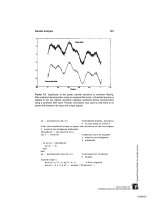
Typical Operating Characteristics
(Vcc
=
12V VOUT
=
1
475V and
Ta
=
+25"C
uslng
clrcult
In
Figure
2. unless othetwse noted
1
ADAPTIVE GATE DELAY
EFFICIENCY VS. OUTPUT CURRENT
90
3
85
$
80
P
::
75
-
>
700
10
20
30
40
50
60
70 80
HIGH-SIDE GATE DRIVES, RISE
I
FALL TIME LOW-SIDE GATE DRIVES, RISE
I
FALL TIME
6
REV
1 1
0
4120105
226
Appendix
A
Fairchild Specifications
for
FAN5093
PRODUCT SPECIFICATION FAN5093
Typical Operating Characteristics
(Continued)
CURRENT SHARING, 30A LOAD
C"%
I/,
,iMW,
C*?
IbilUdr,
OUTPUT RIPPLE, 701 LOAD
CURRENT SHARING, 70A LOAD
C*l
IL,
,SYdR,
'"2
l",iUd",
Tekrlop
,
cb
~~~ ~
a
DROOP VS.
RDROOP
3w
2
50
-
2
2w
I
iM
- -
-
P
1w
0
50
OW
0
5
10
15 20 25
30 35
40
Rdrmp
(Kn)
REV
1 1
0
4/20/05
7
Appendix A Fairchild Specifications
for
FAN5093
227
FAN5093
PRODUCT
SPECIFICATION
Typical Operating Characteristics
(Continued)
START-UP, 40A LOAD
POWER-DOWN, 40A LOAD
LOAD TRANSIENT, 0-40A
C",
lo",
10A,d"
C"2
"O",
CLOSED LOOP RESPONSE, 40A LOAD
50
w
40 150
-
30
120
P
90
L
20
4
10
60
0
30
-10
"
100
lOD0
lW00
IOOODO
LOAD TRANSIENT, 12-52A
cni
80"I
,20&di"i
C*P
"O",
VOUT TEMPERATURE VARIATION
I
I
1501
I
15w
1
499
1496
1497
1496
1495
1
494
0
25
70
100
FREQUENCY
(HZ)
TEMPERATURE
("C)
8
REV
1 1 0
4R0105
228
Appendix A Fairchild Specifications
for
FAN5093
I
REV
1
1
0
4120105
9
PRODUCT
SPECIFICATION
FAN5093
Reference
QTY
Description
Manufacturer
/
Number
Ut
1 IC. PWM.
FAN5093
Fairchild FAN5093
Fairchild FDD6696
01-8
8
NFET.
30V.
50A.
9m3A
D1.2.
3
3
DIOS.
40V.
500mA Fairchild
MBR0540
L1.2
2 IND.
850nH.
30A.
0
9mU inter-Technical SCTA5022A-R85M
L3
ODI
IND.
750nH.
20A.
3
5mU
Inter-Technical
SC4015-R75M
~~ ~
~~ ~ ~ ~~
Application Circuit
.V"W
R1-4.
9
R5-8
R10
R11
i
5
4
7%
5%
4
2
2%.
5%
1
10%
5%
1 10K.
5%
~~~~
.
__
Figure
2.
Application Circuit
far
70A
VRM
9.x
Desktop Application
R12
R13
R14
C1-6
C7-10
1 75OK. 1%
1 13.3K.1%
1
562K.
1%
6
4
~~~
_.
1 Opf,
25V.
10%
X7R
0
luf.
16V.
10% X7R
cout
8
1
2200pf.
6.3V.
20%.
12m3/,
Aluminum Electrolytic
Rubycon
6
3MBZ2200M
Appendix A Fairchild Specifications for FAN5093
229
~~
FAN5093 PRODUCT SPECIFICATION
Application Information
Operation
The FAN5093 Controller
The FAN5093 is
a
programmable synchronous two-phase
DC-DC controller IC. When designed with the appropriate
external components. the FAN5093 can
be
configured to
deliver more than 50A of output current, for VRM 9.x
applications. The FAN5093 functions
as
a
fixed frequency
PWM step down regulator, with
a
high efficiency mode
(E*)
at light load.
Main Control
Loop
Refer to the FAN5093 Black Diagram
on
page
1.
The
FAN5093 consists of two interleaved synchronous buck con-
verters, implemented with summing-mode control. Each
phase has its
own
current feedback, and there is
a
common
voltage feedback.
The two buck converters controlled by the FAN5093 are
interleaved, that is, they
run
180" out of phase.
This
mini-
mizes the RMS input ripple current, minimizing the number
of input capacitors required. It also doubles the effective
switching frequency, improving transient response.
The
FAN5093 implements "summing mode control", which
is different from both classical voltage-mode and current-
mode control It provides superior performance to either by
allowing
a
large converter bandwidth
over
a
wide range of
output loads and external components. No external compen-
sation is required.
The
control loop of the regulator contains two main sections:
the analog control block and the digital control block. The
analog section consists of signal conditioning amplifiers
feeding into a comparator which provides the input to the
digital control block. The signal conditioning section accepts
inputs from a current
sensor
and
a
voltage
sensor,
with the
voltage sensor being common to both phases, and the current
sensor separate for each. The voltage
sensor
amplifies the
difference between the VFB signal and the reference voltage
from the DAC and presents the output to each of the two
comparators. The current control path
for
each phase takes
the difference between its PGND and SW pins when the low-
side MOSFET is
on,
reproducing the voltage
across
the
MOSFET and thus the input current; it presents the resulting
signal to the rame input of its summing amplifier, adding its
signal
to the voltage amplifier's with
a
certain gain. These
two signals
are
thus summed together.
This
sum
IS
then prc-
sented to
a
comparator looking at the oscillator ramp, which
provides the main PWM control signal to the digital control
block. The oscillator ramps
are
180"
out of phase with each
other,
so
that the two phases
are
an
alternately.
The digital control block takes the analog comparator input
to provide the appropriate pulses to the HDRV and LDRV
output pins for each phase. These outputs control the external
power MOSFETs
Response Time
The FAN5093 utilizes leading-edge, not trailing-edge
control. Conventional trailing-edge control turns
on
the
high-side MOSFET at a clock signal, and then turns it
off
when the
error
amplifier output voltage is equal to the ramp
voltage. As a result, the response time of a trailing-edge
converter can he as long as the off-time of the high-side
driver, nearly an entire switching period. The FAN50933
leading-edge control turns the high-side MOSFET on when
the error amplifier output voltage is equal to the ramp volt-
age, and turns it
off
at the clock signal. As
a
result, when
a
transient
occurs,
the FAN5093 responds immediately
by
turning on the high-side MOSFET. Response time is set by
the internal propagation delays, typically
100nsec.
In
worst
case,
the response time
IS
set by the minimum on-time of the
low-side MOSFET, 330nsec.
Oscillator
The FAN5093 oscillator section
N~S
at
a
frequency deter-
mined by a resistor from the RT pin to ground according to
the formula
The
oscillator generates two internal sawtooth ramps, each at
one-half the oscillator frequency, and running 1809 out of
phase with each other. These ramps cause the turn-on time of
the two phases to
be
phased apw.
The
oscillator frequency
of the FAN5093
can
be
programmed from 200KHz
to
2MHz
with each phase running at
l00KHz
to IMHz, respectwely.
Selection of
a
frequency will depend on variou system
performance criteria, with higher frequency resulting
in
smaller components but typically lower efficiency.
Remote Voltage Sense
The FAN5093 has true remote voltage
sense
capability, elim-
inating
errors
due to trace resistance. To utilize remote
sense.
the VFB and AGND pins should he connected as a Kelvin
trace pair to the point
of
regulation, such
as
the processor
pins. The
converter
will maintain the voltage
m
regulation at
that point Care is required in layout of these grounds,
see
the
layout guidelines in this datasheet.
High Current Output Drivers
The FAN5093 contains four high current output drivers that
utilize MOSFETs in
a
push-pull configuration.
Thc
drivers
for the high-side MOSFETs use the BOOT pin far input
power and the
SW
pin for return. The drivers for the law-side
MOSFETs use the VCC pin for input power and the PGND
pin for return. Typically, the BOOT pin will
use
a
charge
pump
as
shown in Figure
2.
Note that the BOOT and VCC
pins are separated from the chip's internal power and ground,
BYPASS and AGND. for switching noise immunity.
10
REV.
1.1.04/20105
230
Appendix A Fairchild Specifications
for
FAN5093
PRODUCT
SPECIFICATION FAN5093
Adaptive Delay Gate Drive
The FAN5093 embodies
an
advanced design that
ensures
minimum MOSFET transition times while eliminating
shoot-through current. It senses the state
of
the MOSFETs
and adjusts the gate drive adaptively to ensure that they
are
never
an
simultaneowly When the high-side MOSFET turns
off, the voltage
on
its
source
begins to fall. When the voltage
there reaches approximately 2.W the low-side MOSFETs
gate drive is applied. When the low-side MOSFET turns
off,
the voltage at the LDRV pin is semed When it drop\ below
approximately 2V. the high-side MOSFETs gate drive is
applied.
Maximum Duty Cycle
In
order to
ensure
that the current-sensing and charge-
pumping work, the FAN5093 guarantees that
the
low-side
MOSFET will
be
on
a
celtain
portion of each period For
low
kquenciea,
this
occurs as
a maximum duty cycle
of
approxi-
mately 90%.
Thus
at
25OKHz.
with
a
period of 4psec. the
law-side will
be
on
at least 4psec
*
10%
=
400nsec. At higher
frequencies, this time might fall
so
low
as
to be ineffective.
The FAN5093 guarantees a minimum low-side on-time
of
approximately 330nsec. regardless of duty cycle.
Current Sensing
The FAN5093 has two independent current semors, one
for
each phase Current sensing is accomplished by measuring
the source-to-drain voltage
of
the low-side MOSFET during
its on-time. Each phase has its
own
powerground pin.
to
per-
mit the phases to be placed in different locations without
affecting measurement accuracy. For best results, It is impor-
tant to connect the PGND and SW pins for each phase
as
a
Kelvin trace pair directly to the
source
and drain, respec-
tively,
of
the appropriate law-side MOSFET. Care
is
required
in the layout
of
these grounds: see the layout guidelines in
this datasheet
Current Sharing
The two independent current
senson
of
the FAN5093 operate
with their independent current control
loops
to guarantee that
the two phases each deliver half of the total output current.
The only mismatch between the two phases
occurs
if there is
a
mismatch between the RDS,~" of the low-stde MOSFETs.
Light Load Efficiency
At light load, the FAN5093
uses
a
number of techniques to
improve efficiency. Because
a
synchronous buck
converter
is
two quadrant, able to both
source
and
sink
current, dung
light load the inductor current will
flow
away from the out-
put and towards the input during
a
portion
of
the switching
cycle. This reverse current
flow
is detected by the FAN5093
as a positive voltage appearing
on
the low-side MOSFET
during its on-time. When reverse current
flow
is detected,
the low-side MOSFET is turned
off
for
the rest
of
the cycle,
and the current instead
flows
through the body diode
of
the
high-side MOSFET, returning the power to the
source.
This
technique substantially enhances light load efficiency.
Short Circuit
(ILIM Pin)
Current Characteristics
The FAN5093 short circuit current characteristic includes a
function that protects the DC-DC converter from damage in
the event
of
a
short
CITCUI~.
The short circuit limit
ib
set with
the RS resistor,
as
given by the formula
with
Isc
the desired output current limit, RT the oscillator
resistor and RDS,~"
one
phase's low-side MOSFET's
on
resistance. Remember to make the RS large enough to
include the effects of initkill tolerance and temperature
vana-
tion
on
the MOSFETs' RDS.~".
Important
Note!
The oscillator frequency must be selected
before selecting the current limit resistor, because the value
of RT
IS
used
in
the calculation of Rs.
When
an
overwrrent
IS
detected. the high-side MOSFETs
are
turned
off,
and the law-side MOSFETs are turned
on.
and
they remain in this state until the measured current through
the low-side MOSFET has returned to
zero
amps. After
reaching
zero,
the FAN5093 re-soft-starts, ensuring that it
can
also
safely turn
on
into
a
short.
A limitation
an
the current sense circuit is that
Isc
*
RDS.,,"
must be
less
that 375mV. To
ensure
correct operation. use
Isc
-
RDS.~"
0
300mV: between 300mV and 375mV, there
will he
some
"on-linearity
in
the short-circuit current not
accounted for in the equation
As
an
example, consider the typical characteristic of the
DC-DC
converter
circuit with two FDP6670AL law-side
MOSFETs (RDS
=
6
5mR maximum at 25°C
*
1.2
at 75°C
=
7.8mR each,
or
3.9mR total) in each phase, RT
=
42.1 KW
(600KHz oscillator) and
a
50KW Rs.
The
converter
exhibit\
a normal
load regulation characteris-
tic
until
the voltage
across
the MOSFETs exceeds the inter-
nal short circuit threshold of50K3/d(3.9mW
*
41.2K3A
-
6.66)
=
47A [Note that this current limit level
can
be
as
high
as
50KW/(3.5mW
*
41.2KW
*
6.66)
=
52A,
if
the MOSFETs
have typical RDS."" rather than maximum, and
are
at 25"C.l
At this point, the internal comparator trips and signals the
contr~ller to leave
on
the low-side MOSFETs and keep off
the high-side MOSFETs. The inductor current decreases,
and
power
is not applied again until the inductor current
reaches OA and the converter attempts to re-softstan.
E'-mode
In
addition, further enhancement in efficiency can be
obtained by putting the FAN5093 into E*-mode. When the
Droop pin is pulled to the 5V BYPASS voltage, the
"A
phase of the FAN5093
IS
completly turned off, reducing
in
half the amount of gate charge power being consumed.
E*-mode can be implemented with the circuit shown
in
Figure
3.
REV. 1.1.04/20/05
11
Appendix A Fairchild Specifications
for
FAN5093
231
FAN5093 PRODUCT SPECIFICATION
FANSOOB.
P,"
6
(Bjgarpl
Go
2N3W
RDAMP
FIINSWI.
IormP.
E.1
Pin
21
HI=E.MODE
Figure
3.
Implementing E'mode Control
Note: The charge pump for the HlDRVs should be based
on
the
"B
phase of the FAN5093, since the
"A"
phase
is
off in
E*-made.
Internal Voltage Reference
The reference included
m
the FAN5093 is
a
precision hand-
gap voltage reference Its internal resistors are precisely
trimmed to provide
a
near zero
temperature coefficient (TC).
Based
on
the reference is the output from an integrated 5-bit
DAC.
The
DAC monitors the
5
voltage identification pins,
VIDO-4, and scales the reference voltage from 1.1OOV to
1.85OV in 25mV steps.
BYPASS Reference
The internal logic of the FAN5093
mns
on
5V. To permit the
1C to
run
with 12V only, tt produces 5V internally with a
linear
regulator, whose output is present
an
the BYPASS pin.
Thispinshouldhe bypassed witha IOOnFcapacitorfarnoise
suppression. The BYPASS pin should not have any external
load attached to it.
Dynamic Voltage Adjustment
The FAN5093
can
have its output voltage dynamically
adjusted to accommodate
low
power modes. The designer
must ensure that the transitions
on
the VID lines all
occur
simultaneously (within less than 500nsec) to avoid false codes
generating undesired output voltages. The Power Good flag
tracks the VID codes, but has
a
5OOpsec
delay transitianing
from high to
low.
this
IS
long
enough to
ensure
that there will
not be any glitches during dynamic voltage adjwtmmt.
Power Good (PWRGD)
The
FAN5093 Power Good function is designed in accor-
dance with the Fentium IV DC-DC converter specifications
and provides a continuow voltage monitor
on
the VFB pin.
The circuit compares the VFB signal to the VREF voltage
and outputs
an
active-low interrupt signal
to
the CPU should
the
power
supply voltage deviate more than
-12%
of its nom-
inal setpoint. The Power Good flag provides
no
control
func-
tions to the FANS093.
Output Enable/Sofi Start (ENABLEISS)
The
FAN5093 will accept
an
open
collectorfITL
signal for
controlling the output voltage. The
low
state disables the
output voltage. When disabled, the PWRGD output
IS
in
the
low
state.
Even
if
an
enable is not required in the circuit, this pin
should have attached a capacitor (typically 100nF) to soft-
start the switching. A softstart capacitor may be approxi-
mately chosen by the formula:
C,,
(1.7+09074~VouT)
D
-
10gA.
2.5
where: tD is the delay time before the output Starts to ramp
tR
is
the ramp time of the output
Css
=
softstart
cap
VOUT
=
nominal output voltage
However, C must
be
100°F.
Programmable Active
DroopTM
The FANS093 features Programmable Active DroopTM: as
the output current increases, the output voltage drops propor-
tionately an amount that can he programmed with
an
exter-
nal resistor. This feature is offered in order to allow
maximum headroom for transient response of the convener.
The current is sensed losslessly by measuring the voltage
across the low-side MOSFET during its
on
time. Consult the
section on current sensing for details. The droop is adjusted
by the droop resistor changing the gain of the current loop.
Note that this method makes the droop dependent
on
the
temperature and initial tolerance of the MOSFET, and the
droop must be calculated taking
account
of these
tolerances.
Given a maximum output current, the amount of droop can
be programmed with
a
resistor
to
ground
on
the droop pin,
according to the formula
with VD~~~ the desired droop voltage, RT the oscillator
resistor.
I,,,
the output current at which the droop is desired,
and RDS.
On
the on-state resistance of
one
phase's low-side
MOSFET.
Important
Nole!
The oscillator frequency must be selected
before selecting the droop resistor, because the value of RT is
used in the calculation of Rmoop.
Over-Voltage Protection
The FAN5093 constantly monitors the output voltage for
protection against over-voltage conditions. If the voltage at
12
REV
1
1.0
4120105
232
Appendix A Fairchild Specifications
for
FAN5093
PRODUCT
SPECIFICATION
FAN5093
the VFEl pin exceeds 2.2V,
an
over-voltage condition is
assumed and the FAN5093 latches
on
the external low-side
MOSFET and latches off the high-side MOSFET. The
DC-DC converter returns to normal operation only after Vcc
has been recycled.
Over Temperature Protection
If the FAN5093 die temperature exceeds approximately
150°C.
the IC shuts itself
off.
It remains off until the temper-
ature has dropped approximately 25'C. at which time it
resumes normal operation.
Component Selection
MOSFET
Selection
This
application requires N-channel Enhancement Mode Field
Effect Transistors Desired characteristics
are
as
follows
*
Low
Drain-Source On-Resistance,
-
RDS.ON
<
lOmR (lower
is
better),
*
Power
package with
low
Thermal Resistance;
*
Drain-Source voltage rating
>
15V.
-
Low
gate charge, especially for higher frequency
operation.
For the low-side MOSFET, the an-resistance (Ros.0~)
IS
the
primary parameter for selection. Because of the small duty
cycle of the high-side, the on-resistance determines the
power dissipation in the low-side MOSFET and therefore
significantly affects the efficiency of the DC-DC converter.
For high current applications, it may be necessary to
use
two
MOSFETs in parallel for the low-side for each phase.
For the high-side MOSFET. the gate charge is
as
imponant
as
the on-resistance, especially with
a
12V input and with
higher switching frequencies. This is because the speed of
the transition greatly affects the
power
dissipation. It may be
a good trade-off to select a MOSFET with
a
somewhat
higher RDS.,,",
If
by
so
doing
a
much smaller gate charge is
available. For high current applications, it may be necesary
to use
two
MOSFETs
In
parallel
far the high-side for each
phase
At the FAN5093.s highest operating frequencies. It may be
necessary to limit the total gate charge of bath the high-side
and low-side MOSFETs together, to aveR excess power dis-
sipation in the IC.
Far details and
a
spreadsheet
an
MOSFET selection, refer to
Applications Bulletin AB-8.
Gate Resistors
Use of
a
gate resistor
on
every MOSFET is mandatory. The
gate resistor prevents high-frequency oscillations caused by
the
trace
inductance ringing with the MOSFET gate
capacitance. The gate resistors should be located Dhvsicallv
as
close to the MOSFET gate as possible.
REV.
1.1.0
4120105
The
gate resistor ah limits the power dissipation inside the
IC, which could otherwise be
a
limiting factor
on
the switch-
ing frequency. It may thus carry significant power, especially
at higher frequencies As an example: The FDB7045L has
a
maximum gate charge of 70°C at 5V, and
an
input capaci-
tance of 5.4nF. The total energy used in powering the gate
during
one
cycle is the energy needed to get it
up
to 5V,
plus
the energy to get it up to
12V
E
=
C)V+iC-AV2
=
70nC.5V+154nF.(12V~5V)2
2
=
482nJ
This
power
IS
dissipated every cycle, and is divided between
the internal resistance of the FAN5093 gate driver and the
gate resistor. Thus,
*
=
131rnW
4.7R
+
0.5R
and each gate resistor thus requires a 114W resistor to
ensure
worst
case
power dissipation.
Inductor Selection
Choosing the value of the inductor is a tradeaff between
allowable ripple voltage and required transient response
A smaller inductor produces greater ripple while producing
better transient
response.
In
any
case,
the minimum induc-
tance
IS
determined by the allnwsble ripple. The first order
equation
(close
approximation) for minimum inductance for
a
two-phase converter is.
where:
Vm
=
Input Power Supply
Vout
=
Output Voltage
f
=
DCDC
converter
switching frequency
ESR
=
Eouivalent
series
resistance of all mtwt caoacitors in
1.
parallel
Vripple
=
Maximum peak to peak output ripple voltage
budget
Schottky Diode Selection
The application circuit of Figure
2
shows
a
Schottky diode,
DI
(D2
respectively),
one
in each phase. They
are
used
as
free-wheeling diodes to
ensure
that the body-diodes
~n
the
low-side MOSFETs do not conduct when the
upper
MOSFET is turning off and the
lower
MOSFETs
are
turning
on.
It is undesirable far this diode to conduct because its high
forward voltage drop and long reverse recovery time
degrades efficiency, and
so
the Schottky provides a shunt
path
for
the current. Since this time duration is extremely
short, being minimized by the adaptive gate delay, the
selection criterion for the diode is that the forward voltage of
13
Appendix A Fairchild Specifications for FAN5093
233
FAN5093
PRODUCT
SPECIFICATION
Figure
4.
Input
Alter
Deskgn Consideratlons and Component
Selection
Additinnsl information
on
design and component selection
may he
found
in
Fairchild's Application Note
59.
PCB
Layout
Guidelines
*
Placement of the
MOSFETs
relative
to
the FANS093
is
critical.
Place
the
MOSFETs
wch that the
Race
length
of
the HIDRV
and
LODRV pinr of the
FAN5093
to
Ihe FET
pates is mmmiied. A long
lead
length
on
these pins
will
caux high
amounts
of ringing due
to
the inductance of the
trace
and
the gate capacitance
of
the FET.
This
noise
radiates throughout the
board.
and. because it
is
\witching
at wch
P
high voltage and frequency, it
is
very difficult to
wpprusr.
*
In
general.
all
of
the nuisy switching lines should
be
kept
away from the
quiet
analog
section of the FAN5OY3. That
ik,
traces that connect to pins
X-17
(MDRV.
HIDRV.
PGND
and BOW) shnuld
be
kept far away
from
the
traces that
connect
to
pins
I
through
7.
and
pins
18-24.
-
Plecr the
0
IpF
decoupling c;ipilciturr
ils
clme to the
FAN5093
pins
as
pwsiblr.
Extra
lead
length
on
there
reduces their ahility
to
rupprar noise.
*
Each power
and
ground pin should have its
uwn
ria
to
the
npprupriate plane.
'This
helps prmide isulation
hetween
pins.
*
Place
the
MOSFET\.
inductor.
and
Schottky
of
a
given
phase
as
close
together
as
pusiblc for the
same
reasons
as
in the
first
bullet
above. Place the input
bulk
capacitors
as
clur
lo
the drains
of
the high
\rdc
MOSFETs
as murrible.
It
is necessary to hare
wme
low
ESR
capaciton at the input
to
the convener.
These
oiipzicitupi deliver current when the
In
addition, placement of a
O.lpF
decoupling
cap
right
on
the drain
of
each high ride
MOSFET
helm
to
SUDD~~SS
high cide
MOShET
\witches
on.
Becaws ofthr inlcrleavmg.
the
number
of
such capitciton
required
I:,
greatly rcduced
from
that
required
for
a
single-phax
huck
converter. Figure
2
shows
3
x
I
SOOpF.
hut the
eruct
number required will vary
with
the
output
\*oltage
and current. according tn the forniula
fur
the
two
phare
FANSW3.
where
DC
is
the duty cycle.
DC
=
Voul
/
Vin.
Capacitor ripple current rating is
a
function
of
ternprature. and
so
the
manufacturer
should
be
eonfilcted
to find nut the ripple
cumnt
rating at the
expected
opcra-
tionul
temperature.
For
details
on
the
de\ign
uf
an input
til-
ier.refer
to
Applicatms Bulletin AB-16.
.
wnic
ot
the high frequency ruhlching
nm$e
on
the input
01.
the
DC-DC
converter.
*
Place
the
output
bulk capaciton
as
close
to
the CPU
as
possible
to
optimim their
ability
to
supply
instantaneous
cumcnt
to
the load in the
event
of
il
current
msient.
Additional space between the output capacitors
and
the
CPll will
idlow
the
parasitic re\irtmw ofthe hoard twer
10
degritdr
the
W-DV ~onvcrier'i petiomiance
under
severe
load
transient conditionr.
causing
higher
wltape
deviation.
For
more detailed information regarding
capacitor
placement.
refer
to
Application
Bulletin
AB-5.
.
A
PC
Board Layout Chtckli\t
is
available from Fairchild
Application\. A\k
for
Appiic,itinn Bulletin AD-
I
I
14
REV.
1.1.04/20/05
Ihe
Schottky
at
the output current
should
br
ICIS
than the
for-
ward
voltage
of
the
MOSFET's
body diode. Powereapahility
is
not
a criterion
for
this device. as its disbarion is
very
\mall.
Output Filter Capacitors
The output bulk capacitors
of
a
convener help determine its
output ripplc
voltage
and its transient
response.
It
has already
been seen in the section on selecting
an
inductor that the
ESR
helps
set
the minimum inductance.
For
most conveners.
the number
of
capacitors required is detecmined
by
the
Iran-
urn1
response ;and the output ripple voltage.
and
these are
determined by the
ESR
and
not
the
capacitance
~aluc.
That
IS.
in
order
to achiwe the necessary
ESR
to
meet the
tran-
Gent
and
ripple requirements. the capacitance wlue required
i\ already very Iarp
The
most
cummonly used choice
far
oulpul hulk cdpocitorr
8,
duntinuin electrrdytio. because
of
their
low
cast
and
Inu
ESR.
The only type
of
aluminum capacitor used should he
those that have an
ESR
rated at
IWkHz.
Consult Application
Bulletin
AB-14
for
detailed information
on
output capacitor
selection.
For
higher frequency applications. particularly those running
the
FAN5093
oscillator at
>IMHL,
Oscon or
ceramic
capact-
tom
may he considered. They have much smaller
ESR
than
comparable electrnlytics.
but
also much
\mailer
capacitance.
The
output capacitance should
also
include a nomher
of
\mdl
value ceramic capacitors placed
di
close
85
pohsihle
10
the
QFOC~SW~:
O.IpF
and
0
OIpF
are
recimmrnded
values.
Input
Fllter
The
DC-DC
convener design may include
an
input inductor
between the system main supply and the converter input
as
shown in Figure
2.
This
inductor serves
to
isolate the
twain
wpply
from
the nokc in the switching portion
of
the
DC-DC
convener. and
to
limit the inrush current inia the input capac-
itom during
power
up.
A
value
of
I3pH
is rccommended.
It
is necessary to hare
wme
low
ESR
capaciton
ill
the input
the
number
of such
capitciton
required
I:,
greatly
rcduced
from that required
for
a
single-phaqe
huck
convener. Figure
2
shows
3
x
I
SOOpF.
hut
the
eruct
numhcr required will vary
riIh
the output
\*ollage
and
current. according
10
the forniula
234
Appendix A Fairchild Specifications
for
FAN5093
PRODUCT SPECIFICATION FAN5093
PC
Motherboard Sample
Layout
and Gerber File Additional Information
A
reterence
de\ign
for
motherboxd !mplemental!on
of
The
FANS093
along
with the PCAD layout
Gerber
file
and
\ilk
wrern
cdn
he
ohmned
thmugh your
local
Fmchild
repre-
\e"latl"e
For
rddiiionrl
mtormrtm
conlac1
your
local
Fdrchild
reprrrrntsliw
FAN5093 Evaluation Board
Fairchild
proride5
an
evaluatmn
hoard
10
\enty the \y\lem
level performance ufthe FANSW3.
It
\ewe\
a!
a
guide
10
performance
expeclalion\
when
uvng
the wpplted
external
component,
and
PCB layout Plea\e
contact
your
Iod
Fairchild rcpre\enlmve
for
an
e\aluat~m
hoard
REV
1
1 0
4120105
15
Appendix A Fairchild Specifications
for
FAN5093
235
FAN5093 PRODUCT SPECIFICATION
Mechanical Dimensions
-
24
Lead
TSSOP
Notes:
t
Dimensioning
and
lolerancing
per
ANSI
Yt4
5M
1982
2
"0
and "E"
do
not
include
mold
flash
Mold
flash
or
protrusions
Shall
not
exceed
006
inch
(0
15mm)
3
'L"
8s
Ihe
length
of
terminal
for
Soldering
lo
a
wbslrate
4
Terminal numbers
are
Shown
lor
reference
Only
5
Symbol
"N’
IS
the
maximum number
of
terminals
I1
OPLANARITY
16
REV
1 1
0
4120105
236
Appendix A Fairchild Specifications
for
FAN5093
Product
Number
1
Description
FAN5093 PRODUCT SPECIFICATION
Package
Ordering Information
DISCLAIMER
FAIRCHILD SEMICONDUCTOR RESERVES THE RIGHT TO MAKE CHANGES WITHOUT FURTHER NOTICE TO
ANY PRODUCTS HEREIN
TO
IMPROVE RELIABILITY
FUNCTION
OR
DESIGN FAIRCHILD
DOES
NOT ASSUME
ANY LIABILITY ARISING OUT
OF
THE APPLICATION
OR
USE
OF ANY PRODUCT OR CIRCUIT DESCRIBED HEREIN
NEITHER DOES IT CONVEY ANY LICENSE UNDER
ITS
PATENT RIGHTS NOR THE RIGHTS OF OTHERS
LIFE
SUPPORT POLICY
FAIRCHILD
S
PRODUCTS ARE NOT AUTHORIZED FOR USE AS CRITICAL COMPONENTS IN LIFE SUPPORT DEVICES
OR SYSTEMS WITHOUT THE EXPRESS WRITTEN APPROVAL OF THE PRESIDENT OF FAIRCHILD SEMICONDUCTOR
CORPORATION As
used herein
1
Life
supporl devices
or
systems are devices or systems
which
(a)
are
intended
for
surgical
implanl
into
the body
or (b) suppoll
or
suslain
life
and
(c)
whose failure
to
perform when properly used
in
accordance with
Instructions lor
use
provided
in
lhe labeling can be
reasonably expected
to
result
in
a significant
injury
of
the
user
2
A
crilical
component
in
any component
01
a
life
suppon
device
or
system whose failure
to
perform
can
be
reasonably expected
lo
cause the failure
01
the life SUPPO~
device or system
01
lo
an&
11s
safety
or
etfectfveness
YMll
la
rcn
ldseml corn
237
238
Appendix
B
Fairchild Specifications
for
FAN4803
-
FAIRCHILD
-
www.fairchildsemi.com
SEMICONDUCTOR
TM
FAN4803
8-Pin PFC and PWM Controller Combo
Features
*
Internally \ynchroni7ed
PFC
and
PWM
in
one
%pin
IC
.
Patented one-pin voltage
emr
amplifier with advanced
input current shaping technique
-
Peak
or
average
current,
continuous
tmort,
leading edge
PFC
(Input
Current
Shaping Technology)
-
High efficiency trailing-edge current
mode
PWM
*
Low
supply cumnls; start-up:
l5mA
typ operating:
ZmA
typ.
Synchronized leading
and
trailing
edge
modulation
-
Reduces
ripple
current in
the
atomge
capacitor
herween
thc
PPC
and
PWM
sections
*
Overvoltagc,
UVLO.
and
brownout
protectam
*
PFC
VcdlVP
with
PFC
Soft Stan
Block Diagram
General Description
The
FAN4803
LS
a
spacc-saving controller
for
power
factor
cornled. switched mode power supplies that
offers
very
low
sfan-up and operating
currents.
Power
Factor
Comaion
(PFC)
offers
the
use
of
rmaller,
lower
CLXI
bulk
capacim.
reduces
power
line
loading
and
sms
on
Ihe
switching
FETs.
and
results m
a
-r
supply fully compli-
ant
to
IEK
1000-3-2
rpecifieations.
The
FAN4803
includes
circuits
fur
the
implemcntatian of
P
leading
edge,
average
cumnl "hooil"
type
PFC
and a trailing edge,
PWM
The
FAN4X03-l'r
PFC
and
PWM
operate
at
the same
frequency.
67kHz.
The
PFC
frequency
of
the
FAN48034
is
rlutomatically
sct
at
half that of the
134kHz
PWM.
This
higher
frequency
allows
the
uscr
In
design with smaller
PWM
components while maintaining the optimum
operating
frcqucncy
far
the
PFC.
An
OVCNOhge comparator shuts
down the
PFC
section
in
the
event
of a sudden decrease in
load. me
PFC
section
also
includes
peak
current
limiting for
enh~ncsd
system reliability.
REV.
1.2.3
4/20/05
Appendix
B
Fairchild Specifications
for
FAN4803
239
Pin
1
Name
PRODUCT SPECIFICATION
FAN4803
Function
Pin Configuration
FAN4803
8-Pin PDlP (PO8)
8-Pln
SOlC
(508)
PFC
OUT
PWM OUT
GNO
vcc
ISENSE
ILlMiT
"EAO
voc
TOP
VIEW
Pin Description
PWM voltage feedback input
Absolute Maximum Ratings
Ahwlute
m,txmuni
raung,
are
thwe
YP~UCI
beyond
which
the
dc\
kce
wuld
be
perindnently
d.imaged
Ahwlute
maximum
rattng\
are
itrw
rattng, only
and
Iuncimal
device
operalion
I\
not
implied
Parameter
I
Min
I
Max
I
Unit
I
40
I
mA
Icc
Current (average)
I
Plastic
DIP
DIQrtlr
cnlr
-,
. .
I
101.11
""mu
Operating Conditions
Temperature Range
FAN4803CS-X
1
0C
to
70C
FAN4803CP-X
I
0C to 70C
2
REV
1
2
3
4120105
240
Appendix
B
Fairchild Specifications for FAN4803
Symbol
I
Parameter
PRODUCT SPECIFICATION FAN4803
Conditions
I
Min
1
TYP
j
MAX
IUNlTS
Output Low Impedance
Output Low Voltage
Output High Impedance
Output High Voltage
RiseiFall Time
1
VEAO
output Current
I
34.0
1
36.5
j
39.0
1
PA
I
Line Regulation
I
IOV<VCC<15V,VEAO=6V
I
1
0.1
1
0.3
1
PA
I
TA
=
25"C, VEAO
=
6V
Vcc OVP
Comoarator
8
15
%
[OUT
=
-1
OOmA
0.8
1.5
V
iOUT
=
-IOmA, VCC
=
8V
0.7
1.5 V
8
15
U
[OUT= 100mA,VCC= 15V 13.5 14.2
V
CL
=
IOOODF
50
ns
Duty Cycle Range
Output Low Impedance
Outout Low Voltaae
FAN4803-2 0-41 0-47 0-50
%
FAN4803-1 0-49.5
0-50
%
8
15
U
IOUT
=
-1
OOmA
0.8
1.5 V
Output High Impedance
Output High Voltage
Rise/Fall Time
~
,~ ,~
,
I
vcc
Clamp Voltage (Vccz)
I
Start-up Current
I
vcc=1Iv.cL=o
I
0.2
I
0.4
I
mA
1
Icc
=
lOmA
I
16.7
I
17.5
I
18.3
1
V
I
IOUT
=
-1 OmA, VCC
=
8V
0.7
1.5
V
8
15
U
lOUT=
IOOmA, VCC
=
15V 13.5 14.2 V
CL
=
IOOOpF 50
ns
Operating Current
Undervoltage Lockout Threshold
Undervoltage Lockout Hysteresis
REV.
1.2
3 4/20/05
VCC
=
15V, CL
=
0
2.5 4
mA
11.5
12 12.5 V
2.4 2.9 3.4 V
~
3
Appendix
B
Fairchild Specifications
for
FAN4803
241
FAN4803
Functional Description
The FAN4803 consists of
an
average current mode boost
Power Factor Corrector (PFC) front end followed by
a
syn-
chronized Pulse Width Modulation (PWM) controller. It is
distinguished from
earlier
combo
conuollen
by its
low
pin
count, innovative input cunent shaping technique. and very
low
stan-up and operating currents. The PWM section is
dedicated to peak current mode operation. It
uses
conven-
tional trailing-edge modulation, while the PFC uses leading-
edge modulation. This patented Leading Edgefhiling Edge
(LETE) modulation technique helps to minimize ripple cur-
rent in the PFC DC buss capacitor.
The FAN4803 is offered in
two
versions The FAN4803-I
operates both PFC and PWM sections at 67kHz. while the
FAN4803-2 operates the PWM section at twice the fre-
quency (134kHz)
of
the PFC. This
allows
the
use
of
smaller
PWM magnetics and output
filter
components, while mini-
mizing switching
losses
in
the PFC stage.
In
addition to power factor correction, several protection fea-
tures have
been
built into the FAN4803. These include soft
start, redundant PFC over-voltage protection, peak current
limiting. duty cycle limit, and under voltage lockout
(UVLO). See Figure
12
for
a
typical application.
Detailed Pin Descriptions
VEAO
This pin provides the feedback path which forces the PFC
output to regulate at the programmed value. It connects to
programming resistors tied to the PFC output voltage and is
shunted by the feedback compensation network.
ISENSE
This pin ties
to
a resistor
or
current sense transformer which
senses the PFC input current. This signal should
be
negative
with respect to the IC ground. It internally feeds the pulse-
by-pulse current limit comparator and the current
sense
feed-
back signal. The
ILIMIT
trip
level
IS
-IV. The
ISENSE
fced-
back is internally multiplied by a gain of four and compared
against the internal programmed ramp
to
set the PFC duty
cycle.
The
intersection
of
the boost inductor current
downslope with the internal programming ramp determines
the boost off-time
VDC
This pin
is
typically tied
to
the feedback opto-collector. It is
tied to the internal 5V reference through a 26kU resistor and
to GND through
a
40kU reqistor
ILIMIT
This pin
IS
tied to the primary side PWM current
sense
resis-
tor
or
Wansfarmer. It provides the internal pulse-by-pulse
current limit far the PWM stage (which
occurs
at
1
5V) and
the peak current mode feedback path far the current made
PRODUCT SPECIFICATION
control
of
the PWM stage. The current ramp
is
offset inter-
nally by
I
.2V and then compared against the opta feedback
voltage to set the PWM duty cycle.
PFC
OUT
and
PWM
OUT
PFC OUT and PWM OUT
are
the high-current power driv-
ers
capable of directly driving the gate of
a
power MOSFET
with peak currents up to ?IA. Bath outputs are actively held
low
when Vcc is below the UVLO threshold level.
vcc
Vcc
IS
the
power
input connection to the IC.
The
Vcc stm-
up current is 150pA
.
The no-load Icc current is 2mA. Vcc
quiescent current
will
include bath the IC biasing currents
and the PFC and PWM output currents. Given the operating
frequency and the MOSFET gate charge (Qg), average
PFC and PWM output currents can be calculated
as
IOUT
=
Qg
x
F. The average magnetizing current required far any
gate drive transformers must
also
be included. The Vcc pin
is also assumed to be proportional to the PFC output voltage.
Internally it
LS
tied to the VccOVP comparator (16.2V)
providing redundant high-speed over-voltage protection
(OVP) of the PFC stage. Vcc
also
ties internally to the
UVLO circuitry, enabling the IC at 12V and disabling it at
9.1V. Vcc must be bypassed with a high quality ceramic
bypass capacitor Dlaced
as
close
as
possible to the IC
. .
Goad bypassing
IS
critical to the proper operation of the
FAN4803.
Vcc
IS
typically produced by
an
additional winding off the
boost inductor
or
PFC Choke, providing a voltage that is pro-
portional to the PFC output voltage. Since the VccOVP max
voltage is 16.2V, an internal shunt limits Vcc overvoltage to
an
acceptable
value.
An external clamp, such as shown in
Figure
I,
is desirable but not necessary.
IN4148
lN4148
1
GND
IN52468
Figure
1.
Optional
Vcc
Clamp
Vcc
IS
internally clamped to 16.7V minimum, 18.3V maxi-
mum. This limits the maximum Vcc that
can
be applied to
the IC while allowing a Vcc which is high enough
to
trip the
VccOVP. The max current through this
zener
is IOmA.
External series resistance
is
required in order to limit the
current through this Zener in the case where the Vcc voltage
exceeds the
zener
clamp level.
4
REV.
1.2.3
4/20/05
242
Appendix
B
Fairchild Specifications
for
FAN4803
PRODUCT
SPECIFICATION
FAN4803
GND
GND
is the reNrn point
fa
all circuits asmiated with
this
pw.
Note: a highqualily,
low
impedance ground is
critical to the proper operation of the
IC.
High frequency
grounding techniques should be used.
Power
Factor
Correction
Power factor correction makes a nonlinear had
look
like a
resistive load to the
AC
line.
For
a
resistor, the current drawn
from the line is in phase with. and proportional to, the line
voltage. This is defined as
a
unity power factor is (one).
A
common
class
of nonlinear
Inad
is the input of
a
most power
supplies, which
use
a
bridge rectifier and capacitive input
fil-
ter ted from the line. Peak-charging effect. which occurs on
the input filter capacitor in such
a
~~pply, causes brief high-
amplitude pulses of current
to
flow
from the
power
line,
rather than a sinusoidal cunent
in
phase with
the
line volt-
age. Such a ~~pply prescnts a
power
factor to the line of less
than one (another wdy
to state this is that it causes significant
current harmonic, to
appear
at its input).
If
the input Current
drawn
by such a supply (or any other nonlinear load) can be
made to
follow
the input volIage in instantaneous amplitude,
it will appear wsistive
to
the
AC
line and
a
unity power
fac-
tor will be achieved.
To hold the input current draw
of
a
device drawing power
from
the
AC
line in phase with, and proportional to.
the
input
voltage, a way
must
be
found
to
prevent that device from
loading
the
line except in proportion to the instantaneous line
voltage. The
PFC section ofthe
FAN4803
uses
a
hoost-
mode
DC-DC
converter to accomplish this. The input to the
converter is the full wave rectified
AC
line voltage. No
fil-
tering ir applied following the bridge rectifier.
so
the input
voltage
to
the hst convener ranges, at twice line frequency.
from zem volts to the pedk vdlue afthe
AC
input and back to
zero.
By
forcing the hoost converter to meet two blmUkd-
neous conditions. it
is
possible to ensure that
the
current thal
the
convener draws from the
pwer
line matches the instan-
taneous line voltage. One of
these
conditions is that the
output voltage of the boost convener must
be
set higher than
the peak value
of
the line voltage
A
commonly used value is
385VDC.
to
allow
for a high line of
270VACRMS.
The other
condition is that the current that the convener is allowed to
draw
from the line at any given insrant must
be
proportional
to
the
line voltage.
Since the boost converter topology in the
FAN4803
PFC
is
of
the current-averaging type.
no
slope compensation is
required.
Leadinglkailing Modulation
Conventional
Pulse
Width Modulation
(PWM)
techniques
employ
trailing edge modulation in which the switch will
turn
ON right after
the
trailing edge
of
the system clock.
The error amplifier output voltage is then compared with the
modulating ramp When the modulating
ramp
reaches the
level of the
error amplifier output voltage, the switch will be
turned
OFF.
When the switch is ON,
thc
inductor current
will
mp
up. The effective
duty
cycle
of
the mailing edge
modulation is determined during the
ON
time of the switch.
Figure
2
shows
a
typical trailing edge control rcheme.
RAMP
Flgure
2.
Typical Tralllng Edge
Control
Scheme.
REV.
1.2.3
4RW05
5
Appendix
B
Fairchild Specifications
for
FAN4803
243
FAN4803 PRODUCT SPECIFICATION
In
the
case
of
leading
edge
modulation, the switch
IS
turned
Om
right at the leading edge of the System clock. When the
modulating ramp reaches the
level
of the
error
amplifier
outwt
voltas,
the switch
will
be turned ON. The effective
Programming Resistor Value
~q~~~i~~
1
value,
the required
programming
resistor
duty-cycle of the leading edge modulation is determined
edge
control scheme.
during the OFF time of the switch Figure
3
Fhows a leading
Rp=V,,,,-V,,,=400V-=
35M
13Mn
(1)
'PGM
One
of the advantages of this control technique is that it
requires only one Fystem clock. Switch
1
(SWI)
turns
OFF
and
Switch
(sw2)
furnS
ON
at
the
SBme
mlze the
momentary
,,no-load"
penad,
thus
lowering
ripple
voltage generated by the switching action. With such
synchronized switching. the ripple voltage of the first stage simplicity'
that
pole
capacitor
dominates
l2OHr
component
of
the PFC's output ripple voltage can be
PFC
voltage
L~~~
ti^^
The voltage-loop bandwidth
must
be set to
less
than
120Hz
to
limit the amount of line current harmonic distonion.
A typical
crossover
frequency
IS
30Hc.
Equation
1,
for
tO
mini-
Is
reduced. Calculation and
evaluation
have shown that
the
reduced by
as
much
Bs
30%
using
this
method,
substantially
Typical Applications
the
error
amplifier gain
at
the loop unity-gain frequency.
providing 45 degrees ofphase mugin. Equation
3
places
a
places
a
pole
at
the crossoyer
frequency'
reducing dlsslpatlan
1"
the hlgh-voltage pFC capacitor,
zero
One
decade
prlar
to
the
pole'
Bode
plots showing
the
overall
gain and phase are shown in Figures
5
and 6 Figure
4
displays
a
Fimplified model af the
voltage
loop.
Pin
RpxVBw,x
AVEAOx
C,,,
~(2xnxf)~
(')
300W
11.3Mn
x
400V
x
0.5V
x
220pF
x
(2
Y
I
Y
30Hz)'
One Pin Error
Amp
CCOW
=
The FAN4803 utilizes
a
one
pin voltage error amplifier in the
PFC section (VEAO). The error amplifier is in reality a
cur-
rent
sink which forces 35pA through the output program-
ming
resistor. The nominal voltage
at
the VEAO pin is 5V.
The VEAO voltage
range
IS
4 to 6V. For a
11.3MU
resistor
chain
to
the
boost output voltage and 5V steady state at the
VEAO, the boost output voltage
would
be 400V.
CCoMp
=
CCoMp
=
16nF
+
CMP
RAMP
CLK
D
U2-
CLK
osc
U4
Figure
3.
Typical
Leading Edge Control Scheme.
6
REV.
1.2
34/20/05
244
Appendix
B
Fairchild Specifications for FAN4803
~~
PRODUCT SPECIFICATION FAN4803
1
(3)
2
XTIX
f
Y
c,,,,
RCOMP
=
=33OkC2
62
8
x
30Hz
x
16nF
1
10
RCOMP
=
CZERO=
2
nn
x
xRc0,,
(4)
'
=016pF
6.28
x
3Hz
x
33CW
CZERO
=
FAN4803
-
11
3M0
RLOAD
220wF
6670 330kG
34pA
0
15pF
'z:';
COMPENSATION
Figure
4.
Voltage Control
Loop
Internal Voltage Ramp
The internal
ramp
current source
is
programmed by way
of
the
VEAO
pin voltage. Figure
7
displays the internal ramp
current
vs.
the
VEAO
voltage. This current source is used
to
develop the internal ramp by charging the internal
30pF
+I21
-10%
capacitor.
See
Figures
10
and
1
I
The
frequency of the
internal programming ramp
1s
set internally to
67kHc.
PFC Current Sense Filtering
In
DCM,
the input current wave shaping technique
used
by
the FAN4803 could
cause
the input cul~ent to
run
away.
In
order
for
this technique to he able to operate properly
under
DCM,
the programming
ramp
mu\t meet the boost
inductor current down-slope at
zero
amps Assuming the
programming
ramp
is
zero
under light load, the OFF-time
will he terminated
once
the inductor current
reaches
zero.
FREQUENCY (Hz)
Figure
5.
Voltage Loop Gain
01
1
10
100
1000
FREOUENCY
(Hz)
Figure
6.
Voltage Loop Phase
01234567
VEAO
IVI
Figure
7.
Internal Ramp Current
vs.
VEAO
REV.
1.2.3
4/20/05
7
Appendix
B
Fairchild Specifications
for
FAN4803
245
FAN4803
PRODUCT SPECIFICATION
Subsequent!)
the
PFC
gate
drive
ix
initiated. eliminating the
>necessary
dcad
time
needed
tor the
DCM
made. This
force5
the
output
to
run
away until
the
Vcc OVP
rhuo down the
PFC.
This situation is
corrected
by
adding
an
ofkt
voltage
to
the current
wnse
signal. which
forces
the duly cycle
tii
rern
at
light loads. This
offset
prevents the PFC fmm
operat-
ing
in the
DCM
;~nd
force5 pulre-skipping
from
('CM
10
no-
duty, avoiding
DMC
operation. External
tiltering
to
the
cur-
rent sense Ggnal helps
to
rmwth
out
the
sense
signal.
expanding
the
operating
range
slightly into the DCM rmgc
hit
this should
be
done carefully,
as
this filtering
also
reduces the hilndwidth
of
the 5ignul feeding
the
pulsu-by-
pulse current
limit
signal.
Figure
9
dirplaya
a
typical circuit
for
adding
ofkt
to
ISENSE
at
light
loads.
PFC
Start-up and
Soft
Start
During
stciidy
state uperuliun VEAO
draws
3SuA.
At
stmt-up
the internal current iniirrar which sink this
current
is defeated
until Vcc reaches IZV. This furccs
the
PFC
emr
voltage
to
Vcc
at the time
that
the
1C is enabled. With leading edge
modulation
Vcc
on
the
VEAO
pin furccs
zero
duty
un
the
PFC
rrutpul.
When selecting
external
compm\ittion
compn-
nmtr
and Vcc supply
CITCUI~S
VEAO
mubt
not
be prevented
from reaching hV prior
to
Vcc
reaching
12V
in the
tum-on
wqequence.
Thi\
will
guarantee
that
the PFC stage will enter
son-start.
Once
Vcc
rcachen
IZV
the
35pA VEAO
cumnt
sink
ii
enahled.
VEAOcompen\srion comp~menrr
are
then
discharged
b)
way
ofths
3Sp.4
current rink unlil the
rteady
shlr
Operating piint is reached.
See
Figure
8.
PFC
Soft
Recovery Following
Vcc
OVP
The FAN4803 assuiiie~
ths~
Vcc
is
penereled lrom
a
wurcc
that is proporrronai
to
the
PtC
output vult~tgc.
Once
thnl
souwe reaches 16.2V the internal current rink tied
to
the
VEAO
pin
IC
diwbled
just as
in
the
soft
stan
turn-un
Flgure
8.
PFC
Soft
Start
sequence.
Once disabled. thc
VEAO
pin charges
HIGH
by
way
ofthe
exicrnal
components
until thc
PFC
duty cyclc
goes
to
zero,
dirnhling the PFC. The Vcc
OVP
resets
once
the Vcc discharges below 16.2V. enabling the
VEAO
CUT-
rent sink and discharging the VEAO eompcnsation
comp-
nenls until
the
steady
state
operating point
i\
mched.
It
should be noted
that.
as
rhown
in
Figure
X.
once
the VEAO
pin
exceeds
6.W
the intrm.tl
ramp
is
defeated. Hecuure
of
this. an
external
Zener
can
be
imtalled
la
reduw
the
maxi-
mum
voltage
tn
which the
VEAO
pin
may
rise
in
a
shutdown
condition. Cliimping the
VEAO
pin externally
to
7.4V will
reduce
the
time
required
For
the VGAO
[rim
to
recover
to
it\
iteady
state
vdue.
UVLO
Once
Vcc
reaches
I2V
hoth the
PFC
and
PWM
arc enahled.
The UVLO threshold
ib
Y
i
V providing
2
YV
of
hysterrri\.
Generating
Vcc
An
internal
clamp
limits overvoltage
to
Vcc.
This
clamp
circuit enwes that the
Vcc OVP
circuitry
of
the
FAN1803
will I'unctian properly
mcr
tolerance and temperature
while
prutccting
the
part
from
voltape
trimaienir. This circuit
allows
the
FAN4803
10
deliver 15V nominal gilc
d"ve
at
PWM
OUT
and
PA
OL!T.
ruficient
10
driw low-cost
ICBTs.
It
15
importdnt
to
limit the current through
the
Zener
ti)
avoid
weheating
or
demoying
11.
This
cm
be
done with
a
single
resistor in
\cries
with the
Vcc
pin.
returned
tn
a
bias supply
of
typically
14V
to
I
8V.
The
rebirror
value
must
be chusen
to
imert
the aperdting currrnl requirement
of
the FAN4XCI3
itsrllt4.0mA
mm)
plus
the
current
rcqumd
by the
two
gale
driver
output*.
Figure
9.
ISENSE
Onset
for
LlgM
Load
Conditions
8
REV.
1.2.3
4PZW05
246
Appendix
B
Fairchild Specifications for FAN4803
PRODUCT SPECIFICATION FAN4803
vcc
OVP
Component Reduction
Vcc
is asumed to be
a
voltage proportivnal to the PFC
output voltage. typically a bootstrap winding
off
the boost
inductor. The
Vcc OVP
comparator
senses
when this volt-
age exceeds
16V.
and terminates the PFC output dr*e while
disabling the
VEAO
current sink. Once the
VEAO
current
sink
is disabled. the
VEAO
voltage will charge unabated,
except
fbr
a diode clamp tv
Vcc.
reducing the PFC
pulse
width.
Once
the
Vcc
rail
has decnased to
below
16.2V
ihe
VEAO
sink
will
be
enabled, discharging external
VEAO
compensation cornplnents until the
steady
state
voltage
is
reached. Given that
15V
on
Vcc
corresponds to
4OOV
on
the
PFC
output.
16V
on
Vcc
corresponds
to
an
OVP
level
of
426V.
Components
aswciated
with the
VRMS
and
IRMs
pins of a
typical PFC controller such as the
MU824
have been elimi-
nated. The PFC puwer
limit
and bandwidth does
vary
with
line
voltage. Double the power can
be
delivered from a
220
V
AC line versus
a
I10
V
AC
line.
Since this
is
a
combina-
tion
PFCIFWM.
the
power to the load
is
limited
by
the PWM
stage
Figure
10.
Typical Peak Current
Mode
Waveforms
Figure
11.
FAN4803 PFC Control
REV.
1.2.3
4/20/05
9
Appendix
B
Fairchild Specifications for FAN4803
247
FAN4803
PRODUCT
SPECIFICATION
I
I1
I
1111
1'1
~igure
12.
~ypicsl Application
circuit.
Unlversal
Input
240W
12v
DC
output
10
REV
1
2
3
4120105
248
Appendix
B
Fairchild Specifications for FAN4803
PRODUCT
SPECIFICATION FAN4803
Mechanical Dimensions
Package
SO8
8
Pin
SOlC
Package PO8
8-Pin PDlP
REV
1
2
3
4120105 11
Appendix
B
Fairchild Specifications for FAN4803
249
FAN4803CS-1 67kHz
/
67kHZ
FAN4803 PRODUCT SPECIFICATION
0°C
to
70°C
8-Pin
SOlC
(SO8)
~
____~
~ ~~ ~~~~~~
Ordering Information
FAN4803CP-1 67kHZ
/
67kHZ
0°C
to
70°C
8-Pin
PDlP
(PO8)
DISCLAIMER
FAIRCHILD SEMICONDUCTOR RESERVES THE RIGHT TO MAKE CHANGES WITHOUT FURTHER NOTICE
TO
ANY PRODUCTS HEREIN TO IMPROVE RELIABILITY
FUNCTION
OR
DESIGN FAIRCHILD DOES NOT ASSUME
ANY LIABILITY ARISING OUT OF THE APPLICATION
OR
USE OF ANY PRODUCT
OR
CIRCUIT DESCRIBED HEREIN
NEITHER DOES
IT
CONVEY ANY LICENSE UNDER
ITS
PATENT RIGHTS NOR THE RIGHTS OF OTHERS
LIFE SUPPORT POLICY
-
-
. . . .
-
.
FAIRCHILD
S
PRODUCTS ARE NOT AUTHORIZED FOR USE AS CRITICAL COMPONENTS IN LIFE SUPPORT DEVICES
OR
SYSTEMS WITHOUT THE EXPRESS WRITTEN APPROVAL OF THE PRESIDENT OF FAIRCHILD SEMICONDUCTOR
CORPORATION AS
used herein
1
Life
support devices
or
systems
are
devices
or
systems
which
(a)
are
intended
lor
surgical implant into the body
or
(b) support
or
susta111
life
and
(c)
whose
failure
to
perform
when
properly used
in
accoidance with
in~tructions
lor
use
provided
in
the
labeling
can
be
reasonably expected to
res~lt
in
a
significant
inpry
of
the
2
A
critical
component
In
any
component
of a life
suppolt
device
or
system
whose
failure
to perform
can be
reasonably
expected tocausethefailure ofthe
life
suppon
device
or
system
or
to
akct
115
safety
or
effectiveness
"*el
ww
fa
rch
,Maem,
Corn