logic synthesis with verilog hdl
Bạn đang xem bản rút gọn của tài liệu. Xem và tải ngay bản đầy đủ của tài liệu tại đây (304.11 KB, 30 trang )
Advanced VLSI Design Lab, IIT Kharagpur
Digital Design Group
Advanced VLSI Design Lab, IIT Kharagpur
Advanced VLSI Design Lab, IIT Kharagpur
Digital Design Group
Digital Design Group
Logic Synthesis with Verilog HDL
Gourav Sarkar
Gourav Sarkar
Advanced VLSI Design Lab, IIT KGP
Advanced VLSI Design Lab, IIT KGP
Contents:
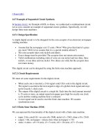
1. What is Synthesis?
2. Synthesis Design Flow.
3. Verilog HDL Synthesis.
4. Interpretation of few Verilog constructs.
5. Verification of the Gate-Level Netlist.
6. Modeling Tips for Logic Synthesis.
7. Impact of Logic Synthesis.
8. Synthesis Tool.
9. An Example.
10.Summary.
Advanced VLSI Design Lab, IIT KGP
Advanced VLSI Design Lab, IIT KGP
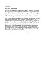
What is Logic Synthesis?
Logic synthesis is the process of converting a high-level
description of the design into an optimized gate-level
presentation, given a standard cell library and certain
design constraints.
Standard cell library: and, or, nor etc.
Design constraints: timing, area, power
Advanced VLSI Design Lab, IIT KGP
Advanced VLSI Design Lab, IIT KGP
Behavioral
Physical
Structural
Synthesis
Physical Design
Advanced VLSI Design Lab, IIT KGP
Advanced VLSI Design Lab, IIT KGP
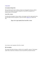
The Verilog Design Flow
Design Specification
Behavioral Description
RTL Description
Functional Verification &Testing
Logic Synthesis
Gate-Level Net list
Logical Verification & testing
Floor Planning, placing & Routing
Physical Layout
Layout Verification
Layout Implementation
Advanced VLSI Design Lab, IIT KGP
Advanced VLSI Design Lab, IIT KGP
LOGIC SYNTHESIS FLOW:
RTL Description
Logic Optimization
Technology Mapping and
Optimization
Translation
Un-optimized Internal
Representation
Optimized Gate-Level
Representation
Design
Constraints
Library of
available gates.
(Technology
Library)
RTL TO GATES
Advanced VLSI Design Lab, IIT KGP
Advanced VLSI Design Lab, IIT KGP
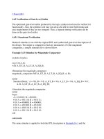
Discussion On Each Block::
RTL description: Design at a high level using RTL constructs.
Translation: Synthesis Tool convert the RTL description to un-
optimized internal representation.
Un-optimized Intermediate Representation: Represented internally
by the logic synthesis tool in terms of internal data structure.
Logic Optimization: Logic is optimized to remove redundant logic.
Technology Mapping and Optimization: Here the synthesis tool
takes the internal representation and implements the representation
in gates, using the cells provided in the technology library.
Advanced VLSI Design Lab, IIT KGP
Advanced VLSI Design Lab, IIT KGP
Technology Library
It contains library cells that can be basic gates or macro cells.
The cell description contains information about the following:
•Functionality of the cell.
•Area of the cell layout.
•Timing information about the cell.
•Power information about the cell.
Advanced VLSI Design Lab, IIT KGP
Advanced VLSI Design Lab, IIT KGP
Design Constraints
It includes the following:
•Timing
•Area
•Power
Area
Timing
Advanced VLSI Design Lab, IIT KGP
Advanced VLSI Design Lab, IIT KGP
Points to note about synthesis
• For very big circuits, vendor technology libraries
may yield non-optimal result.
• Translation, logic optimization and technology
mapping are done internally in the logic synthesis
tool and are not visible to the designer.
• Timing analyzer built into synthesis tools will have
to account for interconnect delays in the total
delay calculation.
Advanced VLSI Design Lab, IIT KGP
Advanced VLSI Design Lab, IIT KGP
Verilog HDL Synthesis
Verilog Constructs:
Ports, Parameters, Signals & variables,
functions & tasks, loops, …
Verilog Operators:
Arithmetic, Logical, Bit-wise, Shift, …
Statements that don’t get Synthesis:
•Primitive definitions.
•Time declaration (#delay).
•Event declaration.
•Case operators (…===…, …!==…)
•Repeat, wait
•… and few more
Advanced VLSI Design Lab, IIT KGP
Advanced VLSI Design Lab, IIT KGP
Interpretation of few Verilog Constructs
The assign statement:
Adder: assign {cout, sum} = a + b + cin;
assign out = (a & b) | c;
Multiplexer: assign out = (s) ? i1 : i0;
The if-else statement
if (s)
out = i1;
else
out = i0;
The case statement
case (s)
1’b0 : out = i0;
1’b1 : out = i1;
endcase
Advanced VLSI Design Lab, IIT KGP
Advanced VLSI Design Lab, IIT KGP
For loops:
for (i=0; i<5;i=i+1)
{c, sum[i]} = a[i] + b[i] + c;
Always statement:
For D- Filp Flop
always @(posedge clk)
q <= d;
always @(clk or d)
if (clk)
q <= d;
Advanced VLSI Design Lab, IIT KGP
Advanced VLSI Design Lab, IIT KGP
Blocking Statements :
Verilog and Synthesis
always @(posedge clk) begin
x = in;
op = x;
end
always @(posedge clk) begin
x <= in;
op <= x;
end
Non-Blocking Statements :
Advanced VLSI Design Lab, IIT KGP
Advanced VLSI Design Lab, IIT KGP
STATE MACHINE HARDWARE
Advanced VLSI Design Lab, IIT KGP
Advanced VLSI Design Lab, IIT KGP
Verification of the Gate-Level Netlist
Functional Verification:
Identical stimulus is run with the original RTL and synthesized
gate-level descriptions of the design. The output is compared to
find any mismatches.
Timing Verification:
Gate-level netlist is checked for timing by use of timing
simulation or by static timing verifier.
Advanced VLSI Design Lab, IIT KGP
Advanced VLSI Design Lab, IIT KGP
Modeling Tips for Logic Synthesis
I. Verilog Coding Style :
1. Use meaningfull names for signals and variables.
2. Avoid mixing positive and negative edge-triggered flip-flops.
3. Use basic building blocks vs. use continuous assign statements.
4. Instantiate multiplexers vs. use if-else or case statements.
5. Use parenthesis to optimize logic structure.
6. Use arithmetic operators *,/ and % vs. design building blocks.
7. Be careful with multiple assignments to the same variable.
8. Define if-else and case statements explicitly.
Advanced VLSI Design Lab, IIT KGP
Advanced VLSI Design Lab, IIT KGP
II. Design Partitioning:
1. Horizontal partitioning.
2. Vertical partitioning.
3. Parallelizing design structure.
III. Design Constraint Specification:
Accurate specification will produce gate-level netlist that is
optimal.
Advanced VLSI Design Lab, IIT KGP
Advanced VLSI Design Lab, IIT KGP
a. Simplification of logic equation.
minimization of boolean expression.
two level (karnaugh map, Quine Mc-clauskey, Espresso).
multilevel
reduce no. of literals.
factoring , common sub-expression.
F(A,B,C,D,E,F,G) = ADF + AEF + BDF + BEF + CDF + CEF + G
= (A + B + C)(D + E)F + G
b. Mapping logic equation to gates.
c. Gate level optimization.
replace OR-NOT by NOR
d. Technology mapping.
Basic Problem
Advanced VLSI Design Lab, IIT KGP
Advanced VLSI Design Lab, IIT KGP
Impact of Logic Synthesis
• No manual conversion, design is describes at the higher
level of abstraction.
• High-level design is done without significant concern about
design constraints.
• Conversion from high-level design to gates is fast.
• Turnaround time for redesign of blocks is shorter.
• Logic synthesis tools optimize the design as a whole.
• Logic synthesis tools allow technology-independent
design.
• Design reuse is possible for technology-independent
descriptions.
Advanced VLSI Design Lab, IIT KGP
Advanced VLSI Design Lab, IIT KGP
Advanced VLSI Design Lab, IIT KGP
Advanced VLSI Design Lab, IIT KGP
Advanced VLSI Design Lab, IIT KGP
Advanced VLSI Design Lab, IIT KGP
Tools used in the lab
Verilog HDL Æ Verilog XL by Cadence
Logic Simulation Æ Simvision by Cadence
Logic Synthesis Æ Design Compiler by Synopsis
Physical Design Æ Silicon Ensemble by Cadence
Advanced VLSI Design Lab, IIT KGP
Advanced VLSI Design Lab, IIT KGP
Important Command
Advanced VLSI Design Lab, IIT KGP
Advanced VLSI Design Lab, IIT KGP
// Multiplexer in verilog
module muxe(data_in,sel,out,clk);
input [3:0] data_in;
input [1:0] sel;
input clk;
output out;
wire [1:0] sel;
wire [3:0] data_in;
reg out;
always @(posedge clk)
begin
case(sel)
2'b00: out=data_in[0];
2'b01: out=data_in[1];
2'b10: out=data_in[2];
2'b11: out=data_in[3];
endcase
end
endmodule
Example of 4X1 Multiplexer
Advanced VLSI Design Lab, IIT KGP
Advanced VLSI Design Lab, IIT KGP