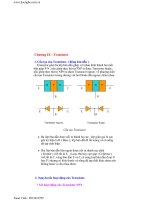
CHƯƠNG 9 ADC-DAC
Bạn đang xem bản rút gọn của tài liệu. Xem và tải ngay bản đầy đủ của tài liệu tại đây (4.81 MB, 39 trang )
Chapter 9
DIGITAL ANALOG CONVERSION
1
Introduco n
An ADC inputs an analog electrical signal such as voltage or current and outputs a binary number. In
block diagram form, it can be represented as such:
2
Introduco n
A DAC, on the other hand, inputs a binary number and outputs an analog voltage or current signal. In
block diagram form, it looks like this:
3
Introduco n
Together, they are often used in digital systems to provide complete interface with analog sensors and
output devices for control systems such as those used in automotive engine controls:
4
Introduco n
It is much easier to convert a digital signal into an analog signal than it is to do the reverse.
Therefore, we will begin with DAC circuitry and then move to ADC circuitry.
5
The R/2
n
R DAC
6
The R/2
n
R DAC
For a simple inverting summer circuit, all resistors must be of equal value.
If any of the input resistors were different, the input voltages would have different degrees of effect
on the output, and the output voltage would not be a true sum.
Let's consider, however, intentionally setting the input resistors at different values. Suppose we were
to set the input resistor values at multiple powers of two: R, 2R, and 4R, instead of all the same value
R
7
The R/2
n
R DAC
8
The R/2
n
R DAC
9
[ ]
REF
1n
F
012n1no
V
R2
R
bb bbV
−
−−
×−=
The R/2
n
R DAC
If we chart the output voltages for all eight combinations of binary bits (000 through 111) input to
this circuit, we will get the following progression of voltages:
Binary Output voltage
000 0.00 V
001 -1.25 V
010 -2.50 V
011 -3.75V
100 -5.00 V
101 -6.25 V
110 -7.50 V
111 -8.75 V
10
The R/2
n
R DAC
We can adjust resistors values in this circuit to obtain output voltages directly corresponding to the
binary input. For example, by making the feedback resistor 800 Ω instead of 1 kΩ, the DAC will
output -1 volt for the binary input 001, -4 volts for the binary input 100, -7 volts for the binary input
111, and so on.
11
The R/2
n
R DAC
with feedback resistor set at 800 ohms
Binary Output voltage
000 0.00 V
001 -1.00 V
010 -2.00V
011 -3.00V
100 -4.00 V
101 -5.00 V
110 -6.00 V
111 -7.00 V
12
The R/2
n
R DAC
If we wish to expand the resolution of this DAC (add more bits to the input), all we need to do is add
more input resistors, holding to the same power-of-two sequence of values:
13
The R/2R DAC
An alternative to the binary-weighted-input DAC is the so-called R/2R DAC, which uses fewer
unique resistor values.
A disadvantage of the former DAC design was its requirement of several different precise input
resistor values: one unique value per binary input bit.
Manufacture may be simplified if there are fewer different resistor values to purchase, stock, and sort
prior to assembly.
14
The R/2R DAC
Of course, we could take our last DAC circuit and modify it to use a single input resistance value, by
connecting multiple resistors together in series:
15
The R/2R DAC
This "ladder" network looks like this:
16
[ ]
REF
n
F
012n1no
V
R2
R
bb bbV ×−=
−−
The R/2R DAC
Either way, you should obtain the following table of figures:
Binary Output voltage
000 0.00 V
001 -1.25 V
010 -2.50 V
011 -3.75V
100 -5.00 V
101 -6.25 V
110 -7.50 V
111 -8.75 V
17
Flash ADC
Also called the parallel A/D converter, this circuit is the simplest to understand.
It is formed of a series of comparators, each one comparing the input signal to a unique
reference voltage.
The comparator outputs connect to the inputs of a priority encoder circuit, which then
produces a binary output.
The following illustration shows a 3-bit *ash ADC circuit:
18
Flash ADC
V
ref
is a stable reference voltage provided by a
precision voltage regulator as part of the converter
circuit, not shown in the schematic.
As the analog input voltage exceeds the reference
voltage at each comparator, the comparator outputs will
sequentially saturate to a high state.
The priority encoder generates a binary number based
on the highest-order active input, ignoring all other
active inputs.
19
Flash ADC
When operated, the flash ADC produces an output that looks something like this:
20
Flash ADC
For this particular application, a regular priority encoder with all its inherent complexity isn't
necessary. Due to the nature of the sequential comparator output states (each comparator saturating
"high" in sequence from lowest to highest), the same "highest-order-input selection" effect may be
realized through a set of Exclusive-OR gates, allowing the use of a simpler, non-priority encoder:
21
Flash ADC
22
Flash ADC
And, of course, the encoder
circuit itself can be made
from a matrix of diodes,
demonstrating just how
simply this converter design
may be constructed:
23
Digital ramp ADC
Also known as the stairstep-ramp, or simply counter A/D converter, this is also fairly easy to
understand but unfortunately suffers from several limitations.
The basic idea is to connect the output of a free-running binary counter to the input of a DAC, then
compare the analog output of the DAC with the analog input signal to be digitized and use the
comparator's output to tell the counter when to stop counting and reset. The following schematic
shows the basic idea:
24
Digital ramp ADC
25