Advanced luminescence based characterisation of silicon wafer solar cells
Bạn đang xem bản rút gọn của tài liệu. Xem và tải ngay bản đầy đủ của tài liệu tại đây (14.09 MB, 213 trang )
ADVANCED LUMINESCENCE-BASED
CHARACTERIZATION OF SILICON WAFER SOLAR
CELLS
Matthew P. Peloso
(B.Sc.(hon), Physics, University of Waterloo)
(GCMOT, Engineering, National University of Singapore)
(M.Sc., Physics, National University of Singapore)
A THESIS SUBMITTED FOR THE DEGREE OF
DOCTOR OF PHILOSOPHY
DEPARTMENT OF ELECTRICAL AND COMPUTER
ENGINEERING
NATIONAL UNIVERSITY OF SINGAPORE
2012
0.1 Acknowledgments
I began my PhD program in the quantum optics group at the Physics Department,
National University of Singapore (NUS). During this period of time I was able to achieve
a long term goal: to work with entangled systems of light, and observe first-hand the Bell
violation. Thanks to Christian Kurtsiefer and Antia Lamas-Linares for making
this possible, and their help in advancing the research. Thanks particularly to Ilja
Gerhardt for his dedicated work, and to Alexander Ling.
Having completed my doctoral coursework and projects in quantum cryptography,
I became interested in working on a project in the applied sciences. Armin Aberle
offered a project at the Solar Energy Research Institute of Singapore in NUS. This
project involved optical characterization of semiconductors using luminescence. This
portion of my doctoral research is presented in this Thesis, whereas the work completed
at the beginning of my doctoral program in the Department of Physics and the Center
for Quantum Technologies is summarized in Section 0.2.
Funding for this project was received from the Singapore International Graduate
Award through the Agency for Science, Technology & Research and NUS, as well as
the Economic Development Board of Singapore. Kind thanks to the funding agencies.
The Renewable Energy Corporation (REC) at Tuas, Singapore supplied the author with
multiple sample devices and material for investigation. Thanks to REC, to their sci-
entists and engineers, including Roland Utama for sample preparation and operating
the Semilab tool.
A special thanks to Peter W
¨
urfel who provided derivations of photoluminescence
spectra, and for valuable discussions on the generalized Planck law. Thanks to Pooja
Chaturvedi for her effort in the characterization lab. A very special thanks to Jen
Sern Lew for developing algorithms and processing data sets for interpretation of lu-
minescence hyperspectral images, and polarization images.
Other thanks go to Marius Peters for algebraic manipulations, to Thorsten
Trupke and others at BT Imaging Pty Ltd for their discussions. Thanks to Jonathan
Hobley for collaboration on lock-in thermography. Thanks to Mark Breese and Ren-
i
qin Min from the Physics Department at NUS for collaboration on x-ray fluorescence
measurements.
Thanks to Noritaka Usami for supplying silicon samples for studies on dislocations
in multicrystals. Thanks to Otwin Breitenstein for discussions and measurements on
defects in silicon wafer solar cells. Thanks also to Sven Riβland for lock-in thermogra-
phy measurements on samples studied using inline photoluminescence characterization
and defect luminescence imaging. Thanks to P&P Optica for completing the initial
demonstration of hyperspectral imaging. Thanks to Photon Etc. for accepting sam-
ples for advanced studies using high resolution hyperspectral imaging, and accepting
modifications to study the polarization interaction of the excitation in their system.
Thanks as well to Masayuki Fukuzawa for accepting silicon wafers for comparative
studies of luminescence images using transmission polarimetery.
Thanks go to everyone who worked in the SERIS characterization lab. Specific thanks
to Keith Punzalan who provided solar energy market data presented in this Thesis.
Thomas Reindl discussed solar systems projects. Jiaji Lin compiled measurements us-
ing the photospectrometer for the home-built EL/PL tool. Thanks to Natalie Palina
who performed detailed analyses of samples using the synchrotron light source. Thanks
to Joachim Luther for discussions on the polarization of light emission. Thanks to Tim
Walsh, Hidayat, and Martin Heinrich for collaborating on ideas, experiments, and
discussing PV technology. Thanks to Wilfred Walsh for discussions on PV markets
and equities. Thanks to my supervisor Armin Aberle and my co-supervisor Bram
Hoex for guidance on the presentation of the scientific results.
Best of luck to you all in your future endeavors.
ii
0.2 Publication list
The following journal articles were published by the author while at the Department of
Electrical and Computer Engineering, National University of Singapore.
• Matthew P. Peloso, Jen Sern Lew, Thorsten Trupke, Marius Peters, and Armin G.
Aberle, Evaluating the electrical properties of multisilicon wafer solar cells using
hyperspectral imaging of luminescence, Applied Physics Letters 99, 221915 (2011)
• Matthew P. Peloso, Jen Sern Lew, Pooja Chaturvedi, Bram Hoex, and Armin G.
Aberle, Polarization analysis for the characterization of defects in silicon wafer
solar cells, Progress in Photovoltaics: Research and Applications, Paper presented
at 26th EU PVSEC, Hamburg, Germany 2011, (in press, DOI: 10.1002/pip.1201)
(2011)
• Matthew P. Peloso, Bram Hoex, and Armin G. Aberle, Polarization analysis for
the characterization of silicon wafer solar cells, Applied Physics Letters 98, 171914
(2011)
The following conferences articles and conference presentations were completed/accepted
while at the Department of Electrical and Computer Engineering, National University
of Singapore.
• Matthew P. Peloso, Jen Sern Lew, Bram Hoex, and Armin G. Aberle, Line-imaging
spectroscopy for characterization of silicon wafer solar cells, Energy Procedia 15,
pp. 171-178 (2012)
• Matthew P. Peloso, Bram Hoex, and Armin G. Aberle, Polarization analysis for the
characterization of defects in silicon wafer solar cells, Proceeding of the 26th Euro-
pean Photovoltaic Solar Energy Conference and Exhibition (PVSEC), Hamburg,
Germany (2011) - plenary talk
• Matthew P. Peloso, Detection of defect densities in raw silicon wafers using a
transmission polarimeter, 38th IEEE Photovoltaic Specialists Conference (PVSC),
Austin, Texas (2012) - conference proceedings and poster presentation (N.B. con-
ference funding withdrawn by SERIS)
• Natalie Palina, Matthew P Peloso, Krzysztof Banas, Bram Hoex, Study on defects
in multicrystalline silicon wafer solar cells by electroluminescence imaging and
synchrotron radiation induced x-ray emission, 1BO.9.5, Oral Presentation, 27th
EU PVSEC (Sept. 2012) - oral presentation accepted
• Matthew P. Peloso, Pooja Chaturvedi, Bram Hoex, and Armin G. Aberle, Effects of
optical instrumentation on the electroluminescence based ratio method for diffusion
length imaging of silicon wafer solar cells, Symposium O of ICMAT 2011, Singapore
(2011) - conference poster presentation
iii
• Matthew P. Peloso, Jen Sern Lew, Bram Hoex, and Armin G. Aberle, Hyperspec-
tral imaging for the spatially resolved characterization of the effective pathlength
enhancement factor of a silicon wafer solar cell, Symposium O of ICMAT 2011,
Singapore (2011) - conference talk
• Matthew P Peloso, Dora Chen, Olga Pawluczyk, Bram Hoex, and Armin G. Aberle,
Spatially resolved optical determination of the path-length enhancement factor of
texturized silicon wafer solar cells, MRS-S Trilateral Conference on Advances in
Nanoscience - Energy, Water & Healthcare, Singapore, (2010) - conference poster
presentation
• Matthew P. Peloso, Pooja Chaturvedi, Peter W¨urfel, Bram Hoex, and Armin
G. Aberle, Observations on the spectral characteristics of defect luminescence of
silicon wafer solar cells, 35th IEEE Photovoltaic Specialists Conference (PVSC),
Hawaii (2010) - conference proceedings and poster presentation
The following work was published and/or completed by the author while at the
Department of Physics and the Center for Quantum Technologies, National University
of Singapore.
• Matthew P Peloso, Ilja Gerhardt, Caleb Ho, Ant´ıa Lamas-Linares, and Christian
Kurtsiefer, Daylight operation of a free space, entanglement-based quantum key
distribution system, New Journal of Physics 11, 045007 (2009) - invited journal
article
• Alexander Ling, Matthew P. Peloso, Ivan Marcikic, Valerio Scarani, Ant´ıa Lamas-
Linares, and Christian Kurtsiefer, Experimental Quantum Key Distribution Based
on a Bell Test, Physical Review A - (Rapid Comm.) 78, 020301 (2008) - journal
article
• Ilja Gerhardt, Matthew P. Peloso, Caleb Ho, Ant´ıa Lamas-Linares, and Christian
Kurtsiefer, Entanglement-based free space quantum cryptography in full daylight,
Conference on Lasers and Electro-Optics (CLEO) / Conference on Quantum Elec-
tronics & Laser Science (QELS) 2 no.4p.1 Jun (2009) - conference proceeding
• Matthew P. Peloso, Ilja Gerhardt, Caleb Ho, Ant´ıa Lamas-Linares, and Christian
Kurtsiefer, Daylight quantum key distribution, 4th Mathematical and Physical
Sciences Graduate Congress, Singapore, 17-19 December, 2008 (conference talk
and paper) - conference talk and proceeding
• Alexander Ling, Matthew P. Peloso, Ivan Marcikic, Ant´ıa Lamas-Linares, and
Christian Kurtsiefer, Experimental E91 quantum key distribution, Advanced Opti-
cal Concepts in Quantum Computing, Memory, and Communication, Proceedings
of the Society of Photo-Optical Instrumentation Engineers (SPIE) 6903 art. no.
69030U p.U9030-U9030 January (2008) - conference proceeding
• Ant´ıa Lamas-Linares, Ivan Marcikic, Caleb Ho, Matthew P. Peloso, and Christian
Kurtsiefer, Free space distribution of entangled photons pairs in daylight condi-
tions, 1-4 CT Pacific Rim Conference on Lasers and Electro-Optics (CLEO), Aug.
26-31, 2007 CL Seoul, South Korea (2007) - conference talk and proceeding
iv
0.3 Overview
Chapter 1 includes an introduction to solar energy, the photovoltaic effect, and solar
cells in Section 1.1, luminescence-based characterization in Section 1.2, and applications
of luminescence characterization to silicon wafer solar cells in Section 1.3.
Chapter 2 gives an overview of optics required to model the silicon material in Sec-
tion 2.2, develops the generalized Planck law of luminescence in Section 2.3, and the
transition moment model of luminescence in Section 2.4. These models are used to in-
terpret luminescence characterization methods for silicon wafer solar cells.
Chapter 3 gives an overview of the instrumentation built to enable electroluminescence
and photoluminescence experiments of silicon wafer solar cells. The instrumentation for
applications of spatially-resolved luminescence spectroscopy is discussed in Section 3.5.2,
and the instrumentation for applications of spatially-resolved luminescence polarimetry
is discussed in Section 3.5.1.
Chapter 4 presents experiments performed for characterization of silicon wafer solar
cells. Diffusion length imaging experiments are presented in Section 4.1. Defect topol-
ogy experiments are presented in Section 4.2, and x-ray fluorescence experiments are
presented in Section 4.3. The later results may be found in articles written by the au-
thor of this Thesis [1, 2].
Chapter 5 presents the results of the spatially-resolved luminescence spectroscopy exper-
iments, with discussion and outlook. This includes applications for studying textured
silicon in Section 5.1, and carrier transport properties in Section 5.2. The results may
be found in articles written by the author of this Thesis [3, 4].
Chapter 6 presents the results of the spatially-resolved luminescence polarization ex-
periments, with discussion and outlook. This includes application to study the partial
polarization of luminescence emission from silicon in Section 6.2, and the orientation of
the polarization of luminescence to silicon defects in Section 6.3. The results may be
found in articles written by the author of this Thesis [5, 6].
Chapter 7 gives a theoretical calculation of the transmission of polarized light at an
edge dislocation in silicon through a crossed polarizer instrument to present an alter-
native methodology for characterization motivated from chapter 6. This provides an
alternative form of optical characterization to photoluminescence, and presents an in-
strument with potential application for raw silicon wafer sorting.
Chapter 8 gives a discussion and outlook based on the experiments and results pre-
sented in the Thesis.
v
Contents
0.1 Acknowledgments . . . . . . . . . . . . . . . . . . . . . . . . . . . . . . . . i
0.2 Publication list . . . . . . . . . . . . . . . . . . . . . . . . . . . . . . . . . iii
0.3 Overview . . . . . . . . . . . . . . . . . . . . . . . . . . . . . . . . . . . . v
0.4 Summary . . . . . . . . . . . . . . . . . . . . . . . . . . . . . . . . . . . . xi
1 Introduction 1
1.1 Solar power . . . . . . . . . . . . . . . . . . . . . . . . . . . . . . . . . . . 1
1.1.1 Sunlight as a source of renewable energy . . . . . . . . . . . . . . . 2
1.1.2 The solar spectrum . . . . . . . . . . . . . . . . . . . . . . . . . . . 5
1.1.3 The photovoltaic effect for direct conversion of sunlight into elec-
tricity . . . . . . . . . . . . . . . . . . . . . . . . . . . . . . . . . . 6
1.1.4 Generation of electrons and holes . . . . . . . . . . . . . . . . . . . 9
1.1.5 Silicon-wafer photovoltaic devices . . . . . . . . . . . . . . . . . . . 10
1.1.6 Defects in silicon wafer solar cells . . . . . . . . . . . . . . . . . . . 13
1.1.7 Characterization of photovoltaic materials and devices . . . . . . . 15
1.2 Luminescence . . . . . . . . . . . . . . . . . . . . . . . . . . . . . . . . . . 17
1.2.1 Introduction to luminescence . . . . . . . . . . . . . . . . . . . . . 17
1.2.2 Generation and detection of luminescence . . . . . . . . . . . . . . 18
1.2.3 A method for developing luminescence-based characterization . . . 20
1.2.4 History of luminescence imaging for gallium arsenide characteri-
zation . . . . . . . . . . . . . . . . . . . . . . . . . . . . . . . . . . 21
1.3 History of luminescence imaging for silicon wafer material and photo-
voltaic device characterization . . . . . . . . . . . . . . . . . . . . . . . . . 22
1.3.1 The spatial homogeneity of a silicon wafer solar cell . . . . . . . . 23
1.3.2 Measuring the electrical properties of a silicon wafer solar cell . . . 25
1.3.3 Identification of defects in solar cells . . . . . . . . . . . . . . . . . 27
1.4 Advancing luminescence-based characterization of silicon wafer materials
and devices . . . . . . . . . . . . . . . . . . . . . . . . . . . . . . . . . . . 29
2 Modeling light emission from silicon 31
2.1 Light and optics . . . . . . . . . . . . . . . . . . . . . . . . . . . . . . . . 31
2.2 Optical properties of silicon . . . . . . . . . . . . . . . . . . . . . . . . . . 32
2.2.1 Refractive index of silicon . . . . . . . . . . . . . . . . . . . . . . . 33
2.2.2 Reflectivity of silicon . . . . . . . . . . . . . . . . . . . . . . . . . . 34
2.2.3 Absorptivity of silicon . . . . . . . . . . . . . . . . . . . . . . . . . 36
2.3 The generalized Planck law of luminescence . . . . . . . . . . . . . . . . . 37
2.3.1 The classical spectrum of luminescence emission . . . . . . . . . . 38
vi
2.3.2 Effect of instrumentation on the measured luminescence . . . . . . 39
2.3.3 Excess carrier concentration . . . . . . . . . . . . . . . . . . . . . . 39
2.3.4 Solving electroluminescence boundary conditions . . . . . . . . . . 41
2.3.5 Solving photoluminescence boundary conditions . . . . . . . . . . . 45
2.3.6 Solving reabsorption of luminescence of a planar cell . . . . . . . . 48
2.3.7 Reabsorption of luminescence in textured wafers . . . . . . . . . . 51
2.4 The transition moment model of light emission . . . . . . . . . . . . . . . 53
2.4.1 The transition moment of light emission . . . . . . . . . . . . . . . 54
2.4.2 Emission processes in the quantum theory . . . . . . . . . . . . . . 55
2.4.3 Luminescence emission from silicon as an oscillation . . . . . . . . 57
2.4.4 Light-matter interactions . . . . . . . . . . . . . . . . . . . . . . . 58
2.4.5 Electrodynamics for light-matter interactions . . . . . . . . . . . . 58
2.4.6 The Hamiltonian of a charge in an electromagnetic field . . . . . . 59
2.4.7 The electric dipole approximation and the transition moment . . . 61
2.4.8 Dependence of the spatial orientation of the charges on the emission 62
2.4.9 The orientation of fields in the light-matter interaction . . . . . . . 62
3 Instrumentation for photoluminescence and electroluminescence ap-
plied to silicon wafer solar materials and devices 64
3.1 Luminescence imaging instrumentation . . . . . . . . . . . . . . . . . . . . 64
3.1.1 Electroluminescence instruments . . . . . . . . . . . . . . . . . . . 64
3.1.2 Photoluminescence instruments . . . . . . . . . . . . . . . . . . . . 67
3.2 Electrical components . . . . . . . . . . . . . . . . . . . . . . . . . . . . . 67
3.2.1 Temperature controller, electrical contacts, and power supply . . . 67
3.3 Optical components . . . . . . . . . . . . . . . . . . . . . . . . . . . . . . 68
3.3.1 Sources of optical excitation . . . . . . . . . . . . . . . . . . . . . . 69
3.3.2 Homogenization of laser light . . . . . . . . . . . . . . . . . . . . . 70
3.3.3 Camera selection . . . . . . . . . . . . . . . . . . . . . . . . . . . . 71
3.3.4 Optical filtering . . . . . . . . . . . . . . . . . . . . . . . . . . . . . 72
3.3.5 Imaging optics . . . . . . . . . . . . . . . . . . . . . . . . . . . . . 74
3.4 Mechanical components . . . . . . . . . . . . . . . . . . . . . . . . . . . . 75
3.5 Modifications to the luminescence-imaging instruments for advanced char-
acterization of silicon wafer solar cells . . . . . . . . . . . . . . . . . . . . 76
3.5.1 Luminescence polarimetry instrument . . . . . . . . . . . . . . . . 77
3.5.2 Luminescence spectroscopy instrument . . . . . . . . . . . . . . . . 78
4 Applications of luminescence imaging of silicon wafer solar cells 82
4.1 Measuring the diffusion length of solar cells using electroluminescence
imaging . . . . . . . . . . . . . . . . . . . . . . . . . . . . . . . . . . . . . 82
vii
4.1.1 The ratio method for imaging diffusion lengths of silicon wafer
solar cell . . . . . . . . . . . . . . . . . . . . . . . . . . . . . . . . . 82
4.1.2 Application of diffusion length imaging using different cameras and
interference filters . . . . . . . . . . . . . . . . . . . . . . . . . . . 84
4.1.3 Ratio images of multicrystalline silicon wafer solar cells . . . . . . 87
4.1.4 On the practical application of diffusion length imaging based on
the ratio method . . . . . . . . . . . . . . . . . . . . . . . . . . . . 89
4.2 Luminescence emission related to defects in silicon wafer solar cells . . . . 90
4.2.1 Reverse-bias luminescence and sub-bandgap luminescence . . . . . 90
4.2.2 Using voltage control and spectral analysis to enhance electrolu-
minescence imaging . . . . . . . . . . . . . . . . . . . . . . . . . . 93
4.2.3 Results from the luminescence investigations and their association
with defects in silicon wafer solar cells . . . . . . . . . . . . . . . . 95
4.2.4 Summary of the investigations of defect luminescence from silicon
wafer solar cells . . . . . . . . . . . . . . . . . . . . . . . . . . . . . 96
4.3 Elemental analysis of defects in silicon wafer solar cells correlated to their
luminescence characteristics . . . . . . . . . . . . . . . . . . . . . . . . . . 96
4.3.1 Luminescence from defects in silicon wafer solar cells . . . . . . . . 97
4.4 Analysis using synchrotron light source for x-ray fluorescence measurements 99
4.4.1 Experimental results from SRIXE analysis . . . . . . . . . . . . . . 99
4.4.2 Summary and discussion on defect luminescence and x-ray fluo-
rescence studies on multicrystalline silicon wafer solar cells . . . . 101
5 Luminescence spectroscopy for characterization of silicon wafer solar
cells 103
5.1 Evaluation of the textured silicon wafer solar cell using luminescence spec-
troscopy . . . . . . . . . . . . . . . . . . . . . . . . . . . . . . . . . . . . . 103
5.1.1 Dependence of the luminescence spectrum on the pathlength en-
hancement factor . . . . . . . . . . . . . . . . . . . . . . . . . . . . 104
5.1.2 Measuring pathlength enhancement of textured solar cells with a
hyperspectral imaging instrument . . . . . . . . . . . . . . . . . . . 105
5.1.3 Fitting procedures on the measured spectra . . . . . . . . . . . . . 108
5.1.4 Resulting measured spectra of the textured samples . . . . . . . . 109
5.1.5 Discussion on the evaluation of the pathlength enhancement factor
using luminescence spectroscopy . . . . . . . . . . . . . . . . . . . 112
5.2 Determining the electrical properties of a multicrystalline silicon wafer
solar cell with a hyperspectral imaging instrument . . . . . . . . . . . . . 112
5.2.1 Quantifying the luminescence spectrum . . . . . . . . . . . . . . . 114
viii
5.2.2 Developing characterization of diffusion length of minority charge
carriers from the luminescence spectrum . . . . . . . . . . . . . . . 117
5.2.3 Sample preparation and experimental procedures for luminescence
spectroscopy . . . . . . . . . . . . . . . . . . . . . . . . . . . . . . 118
5.2.4 Data processing procedures for the spatially-resolved luminescence
spectra . . . . . . . . . . . . . . . . . . . . . . . . . . . . . . . . . 120
5.2.5 Resulting diffusion length images based on the spatially resolved
luminescence spectra . . . . . . . . . . . . . . . . . . . . . . . . . . 122
5.3 Summary and conclusion on spatially-resolved luminescence spectroscopy
of silicon wafer solar cells . . . . . . . . . . . . . . . . . . . . . . . . . . . 123
6 Polarization analysis of luminescence for characterization of silicon
wafer solar cells 125
6.1 The nature of polarization anisotropy of emission . . . . . . . . . . . . . . 125
6.1.1 Spatial anisotropy of defects in silicon . . . . . . . . . . . . . . . . 127
6.1.2 Extended defects in multicrystalline silicon . . . . . . . . . . . . . 128
6.1.3 Polarized emission from a dipole oscillator . . . . . . . . . . . . . . 129
6.1.4 Dislocation emission from multicrystalline silicon . . . . . . . . . . 131
6.2 Partial polarization images of silicon wafer solar cells . . . . . . . . . . . . 134
6.2.1 Experimental procedure used to perform polarization analysis on
defect luminescence . . . . . . . . . . . . . . . . . . . . . . . . . . 135
6.2.2 Resulting analysis of polarization analysis and electroluminescence
images . . . . . . . . . . . . . . . . . . . . . . . . . . . . . . . . . . 136
6.3 Orientation of the polarization of luminescence from dislocations in mul-
ticrystalline silicon solar cells . . . . . . . . . . . . . . . . . . . . . . . . . 139
6.3.1 On the anisotropy of the Bloch bands at extended defects in silicon
wafers . . . . . . . . . . . . . . . . . . . . . . . . . . . . . . . . . . 145
6.4 Conclusion and outlook of luminescence polarimetry of silicon wafer solar
cells . . . . . . . . . . . . . . . . . . . . . . . . . . . . . . . . . . . . . . . 146
7 Theory of defect detection in raw silicon wafers using transmission
polarimetry 148
7.1 Introduction and motivation for the use of transmission polarimetry for
wafer sorting . . . . . . . . . . . . . . . . . . . . . . . . . . . . . . . . . . 148
7.1.1 Comparing transmission polarimetery with photoluminescence imag-
ing . . . . . . . . . . . . . . . . . . . . . . . . . . . . . . . . . . . . 150
7.1.2 Calculation of the transmission of light through a cross polarizer
arrangement including a raw silicon wafer . . . . . . . . . . . . . . 152
ix
7.1.3 Determining the dislocation density in a raw silicon wafer using a
transmission polarimeter . . . . . . . . . . . . . . . . . . . . . . . . 155
7.2 Transmission polarimetry instrument for analysis of the density of ex-
tended defects in silicon wafers . . . . . . . . . . . . . . . . . . . . . . . . 157
7.3 Summary of the potential use of transmission polarimetry for raw wafer
sorting . . . . . . . . . . . . . . . . . . . . . . . . . . . . . . . . . . . . . . 159
8 Conclusion 160
8.1 Discussion . . . . . . . . . . . . . . . . . . . . . . . . . . . . . . . . . . . . 160
8.1.1 Luminescence spectroscopy . . . . . . . . . . . . . . . . . . . . . . 160
8.1.2 Luminescence polarimetry . . . . . . . . . . . . . . . . . . . . . . . 161
8.1.3 Identification of defects in silicon wafer materials and devices . . . 161
8.1.4 Textured silicon materials . . . . . . . . . . . . . . . . . . . . . . . 162
8.2 Proposed future work . . . . . . . . . . . . . . . . . . . . . . . . . . . . . 162
8.2.1 Using polarization of emission to characterize extended defects in
silicon crystals . . . . . . . . . . . . . . . . . . . . . . . . . . . . . 163
8.2.2 Interaction of luminescent materials with alternative external fields 164
8.2.3 Characterization of decorated dislocations and precipitates by cir-
cular or elliptical polarization of luminescence . . . . . . . . . . . . 164
8.2.4 Inline characterization using transmission polarimetry . . . . . . . 165
8.2.5 Spatially-resolved characterization of pathlength enhancement of
textured silicon wafers . . . . . . . . . . . . . . . . . . . . . . . . . 165
8.2.6 Imaging diffusion lengths and the surface recombination velocity . 166
8.2.7 Luminescence emission from thin film devices . . . . . . . . . . . . 166
References 168
x
0.4 Summary
Luminescence-based characterization of silicon wafers and silicon solar cells used to cre-
ate photovoltaic modules for solar energy conversion may reduce their production cost
and performance variance, and allow improved understanding of their physical proper-
ties. Luminescence measurements are advantageous since they are non-destructive, and
provide rapid, spatially-resolved evaluation of large areas typical of silicon photovoltaic
materials and devices, and in room temperature conditions. A luminescence measure-
ment is made by exciting a material or device and recording the emitted electromagnetic
radiation. Luminescence was commonly used more than thirty years ago to image gallium
arsenide substrates for fabrication of integrated circuits. Recently, electroluminescence
and photoluminescence has been used to characterize silicon wafer-based photovoltaic
materials and devices.
In this Thesis, the practical instrumentation of a luminescence imaging system was in-
vestigated to advance luminescence-based characterization of silicon wafer materials, and
silicon wafer photovoltaic devices. A photo/electroluminescence instrument was built to
allow flexible modification of instrumentation parameters to design and test modifica-
tions and applications of the instrument for silicon wafer solar cell characterization.
Two major modifications to luminescence imaging instrumentation for characterization
of silicon photovoltaic materials and devices includes the advancement of polarimetry
for luminescence, as well as the application of hyperspectral imaging of luminescence to
allow luminescence spectroscopy measurements.
The instrument was applied to characterize defects in multicrystalline silicon wafer
solar cells. Both forward and reverse-biasing was applied to the photovoltaic devices
to yield defect-related luminescence. The spatial topography of the defects was inves-
tigated using x-ray fluorescence, and it was found that certain luminescence signatures
correspond with large concentrations of metals, while other signatures were associated
with extended defects in the crystal lattice, particularly dislocations. Spectral imaging
was used as well to evaluate the electrical properties of silicon wafer solar cells.
The application of luminescence spectroscopy using a hyperspectral imaging instru-
xi
ment allowed full area device characterization. Using the generalized Planck law to
compute luminescence spectra over the indirect bandgap of silicon, it was shown that
spectroscopy has advantages over intensity imaging because physical device parameters
may have a distinct affect on the spectral signature of luminescence. This may allow un-
ambiguous and independent determination of a particular device parameter from other
parameters, which otherwise could simultaneously affect the luminescence intensity. As
an example, it was shown that by observing a specific feature of the luminescence spec-
trum, being the wavelength at the peak luminescence intensity, the diffusion length of
minority carriers in the absorber layer can be determined.
The application of polarization-resolved luminescence imaging showed that lumines-
cence polarization is related to extended defects in silicon crystals. The polarization
of emission was shown to correlate strongly with the orientations of extended defects
in silicon crystals, like dislocations and sub-grain boundary dislocation networks. The
physical interpretation of luminescence polarization from dislocation defects in photo-
voltaic devices relates to a electric dipole model of light emission assuming a constrained
oscillator orientation at the structural defect. This oscillator orientation is related thus
to the orientation and structure of extended defects in the raw silicon wafers and ingots
used to fabricate silicon wafer solar cells. This form of characterization may be further
developed to characterize silicon crystalline materials, the physics of solid state light
emission, anisotropic defect structures in crystals, and how to detect these defects to
control device and material fabrication.
xii
List of Tables
1 Characterization methods of solar cells . . . . . . . . . . . . . . . . . . . . 17
2 Types of luminescence . . . . . . . . . . . . . . . . . . . . . . . . . . . . . 18
3 Observable parameters of luminescence . . . . . . . . . . . . . . . . . . . . 19
4 Optical properties of crystalline silicon at room temperature . . . . . . . . 31
5 Sellmeier coefficients for silicon . . . . . . . . . . . . . . . . . . . . . . . . 34
6 Parameters of the fitted spectra for textured samples . . . . . . . . . . . . 111
List of Figures
1.1.1 The sun is the source of solar power . . . . . . . . . . . . . . . . . . . . . 3
1.1.2 AM0 and AM1.5 intensity spectra . . . . . . . . . . . . . . . . . . . . . . 5
1.1.3 The photovoltaic effect in a pn junction solar cell . . . . . . . . . . . . . . 7
1.1.4 I-V curve of a solar cell based on a diode model . . . . . . . . . . . . . . . 8
1.1.5 Solar energy market data 2009 . . . . . . . . . . . . . . . . . . . . . . . . 10
1.1.6 Manufacturing process for silicon wafer solar cells . . . . . . . . . . . . . . 11
1.1.7 A multicrystalline silicon wafer and solar cell . . . . . . . . . . . . . . . . 12
1.1.8 Defects in solar cells . . . . . . . . . . . . . . . . . . . . . . . . . . . . . . 14
1.1.9 Two diode circuit model of a solar cell . . . . . . . . . . . . . . . . . . . . 16
1.2.1 Control-response layout for luminescence characterization . . . . . . . . . 21
1.3.1 Electroluminescence image of a multicrystalline silicon wafer solar cell . . 24
1.3.2 Quantitative series resistance image of a multicrystalline silicon wafer so-
lar cell . . . . . . . . . . . . . . . . . . . . . . . . . . . . . . . . . . . . . . 26
2.2.1 Refractive index of silicon . . . . . . . . . . . . . . . . . . . . . . . . . . . 33
2.2.2 Reflection internal to silicon . . . . . . . . . . . . . . . . . . . . . . . . . . 35
2.2.3 Absorption of light in silicon . . . . . . . . . . . . . . . . . . . . . . . . . 36
2.3.1 Ray paths of luminescence in a planar sample . . . . . . . . . . . . . . . . 50
2.3.2 Ray paths of luminescence in a textured sample . . . . . . . . . . . . . . . 52
3.1.1 Experimental layout for photoluminescence and electroluminescence . . . 65
3.1.2 Electrode assembly for electroluminescence contact . . . . . . . . . . . . . 66
3.2.1 Photo of the photoluminescence experiment . . . . . . . . . . . . . . . . . 68
3.3.1 Coupling and homogenization of the 532 nm photoluminescence laser . . . 69
3.3.2 Homogenizer assembly for the excitation laser . . . . . . . . . . . . . . . . 71
3.3.3 Typical quantum efficiencies of scientific cameras . . . . . . . . . . . . . . 73
3.4.1 Photographs of the assembly for a luminescence imaging instrument . . . 76
3.5.1 Experiment for partial polarization imaging of luminescence from solar cells 77
3.5.2 A spectrum obtained using hyperspectral imaging . . . . . . . . . . . . . . 79
3.5.3 Setup of the hyperspectral imaging spectrometer . . . . . . . . . . . . . . 81
xiii
4.1.1 Ratios of luminescence spectra dependent on the diffusion length . . . . . 83
4.1.2 Measured short and long pass filters used to analyze luminescence . . . . 84
4.1.3 Quantum efficiencies of three cameras and the electroluminescence spectrum 86
4.1.4 LBIC measurements on two multicrystalline silicon wafer solar cells . . . . 86
4.1.5 Ratio of spectral electroluminescence images of multicrystalline silicon
solar cells . . . . . . . . . . . . . . . . . . . . . . . . . . . . . . . . . . . . 88
4.2.1 Quantum efficiencies and filter transmissions for the defect luminescence
measurements . . . . . . . . . . . . . . . . . . . . . . . . . . . . . . . . . . 90
4.2.2 Comparing reverse-bias and sub-bandgap luminescence . . . . . . . . . . . 91
4.2.3 Spectral analysis of reverse-bias luminescence . . . . . . . . . . . . . . . . 92
4.2.4 Sub-bandgap and diode breakdown luminescence image . . . . . . . . . . 94
4.3.1 Defect luminescence of a multicrystalline silicon wafer solar cell studied
using SRIXE . . . . . . . . . . . . . . . . . . . . . . . . . . . . . . . . . . 98
4.4.1 Calibrated SRIXE spectra . . . . . . . . . . . . . . . . . . . . . . . . . . . 100
5.1.1 Electroluminescence of the textured solar cell . . . . . . . . . . . . . . . . 107
5.1.2 Visible and electroluminescence images of textured/untextured solar cells 108
5.1.3 Average textured vs. untextured spectra . . . . . . . . . . . . . . . . . . . 110
5.1.4 Fit parameters obtained using hyperspectral imaging . . . . . . . . . . . . 111
5.2.1 Example fits on a luminescence spectrum . . . . . . . . . . . . . . . . . . 113
5.2.2 LBIC, electroluminescence, and hyperspectral imaging data . . . . . . . . 116
5.2.3 Diffusion length image derived from the peak wavelength . . . . . . . . . 119
5.2.4 Integral ratios on two regions of the spectrum . . . . . . . . . . . . . . . . 123
6.1.1 A dipole emitter . . . . . . . . . . . . . . . . . . . . . . . . . . . . . . . . 127
6.1.2 Differential polarization image . . . . . . . . . . . . . . . . . . . . . . . . . 130
6.1.3 Defect sub-levels in the silicon bandgap . . . . . . . . . . . . . . . . . . . 132
6.1.4 Spatially resolved electroluminescence and sub-bandgap luminescence . . 132
6.1.5 Photoluminescence image of a multicrystalline Si wafer . . . . . . . . . . . 133
6.2.1 Electroluminescence and sub-bandgap luminescence from dislocations in Si137
6.2.2 Partial polarization of sub-bandgap luminescence from a Si wafer solar cell 138
6.3.1 Intensity vs. analyzer angle for luminescence from dislocations . . . . . . 140
6.3.2 Partial polarization and orientation of the polarization . . . . . . . . . . . 142
6.3.3 Orientation of the partial polarization . . . . . . . . . . . . . . . . . . . . 143
6.3.4 Partial polarization, polarization orientation, and polarization contrast . . 144
7.1.1 Stress fields at an edge dislocation . . . . . . . . . . . . . . . . . . . . . . 149
7.1.2 Polar plot of normalized transmission intensity at an edge dislocation . . 153
7.1.3 Transmitted intensity contours for various polarizer angles . . . . . . . . . 156
7.2.1 Instrumentation for transmission polarimetry of silicon wafers . . . . . . . 158
xiv
1 Introduction
1.1 Solar power
Global energy markets are evolving. Conventional energy sources, being fossil fuels, are
becoming more expensive and harder to extract [7]. Particularly, oil prices have risen
significantly, while oil exploration has focused towards unconventional mineral deposits
[8–11]. Combustion of fossil fuels pollutes the atmosphere, and might contribute to global
warming [12]. Thus, many nations today have targets to allocate renewable energy into
their energy production mix [13–15]. Renewable energy is generated using a source that
is not depleted, depletes at a slow rate, or is naturally replenished in a short time [12, 16].
Of renewable energies, solar energy has seen considerable growth since the start
of the millennium [17]. Recently, solar energy has approached costs that make it a
candidate for large-scale application [18, 19]. Policy mandates supporting renewable
energy are a primary motivator for the expansion of photovoltaic energy systems used
for electricity generation
1
[14, 21, 22]. For example, feed-in tariffs allow guaranteed
pricing to give financial certainty to investors, and priority grid access for renewable
energy producers [14, 23]. Solar energy is currently approaching a dollar-per-Watt price
figure, which is decreasing [24]. By most accounts, solar power generation is predicted to
reach dynamic grid parity
2
during this decade. Dynamic grid parity has been achieved
in some equatorial regions, and is expected to be achieved in most equatorial regions as
early as the year 2014 [27].
Solar power is abundant, clean, and has other considerable advantages [21, 28, 29].
Its use allows the containment of waste and pollution at the manufacturing site. A
solar module is non-toxic, and can be recycled. Solar modules last for > 20 years
in the field [30], and generally come with warranties of twenty five years [29]. Solar
photovoltaic modules produce no noise, and allow energy systems to be scaled to larger
power generation capacities if needed. Sunlight provides a large amount of energy every
1
Note, however, that almost all energy generation technologies receive some form of policy support
since energy generation is positively correlated to the economic output and quality of life of a state
[16, 20].
2
For a definition of dynamic grid parity see Luther, Lund or Bhandari [21, 25, 26]
1
day which is free to use, and assessable to all. Solar energy incident on the earth is
orders of magnitude larger
3
than the energy consumed by humankind currently, and
rates foreseeable for some time to come [31].
In this Section, the energy density of sunlight is calculated, and characterized by its
energy spectrum. Devices which use the photovoltaic effect to convert sunlight directly
into electricity are introduced, then luminescence-based characterization of these devices
is introduced.
1.1.1 Sunlight as a source of renewable energy
The sun (see Fig. 1.1.1) generates energy through the fusion of hydrogen atoms due to
the large pressure and temperature in its core. Fusion involves the binding of nuclei into
larger groups. In the sun, hydrogen atoms bind to form helium atoms. The sun is a
spectral class G2V star; a main-sequence star of spectral class G and luminosity class
V [32]. It is known colloquially as a yellow dwarf, emitting primarily yellow and green
light. A yellow dwarf has a temperature of 5300 K and 6000 K at its outer surface, and
a mass of 1.6 × 10
30
kg to 2.38 × 10
30
kg.
The sun is brighter than 85% to 90% of the stars in the Milky Way galaxy, and
provides the majority of energy used by humankind and nature. Energy is released by
the sun into space in the form of electromagnetic radiation. This radiation flux is so
enormous that approximately 1 hour of its energy flow through the earth’s cross-section
is equivalent to the annual worldwide energy consumption of humankind, based on an
estimation of
474 × 10
18
J ≈ 132, 000 T W h (1.1.1)
used in the year 2008
4
.
Sunlight’s energy density may be calculated using the fusion process, the rate that
hydrogen is consumed in the sun, and the geometry of the solar system. The fusion
3
Approximately 10
4
times more sunlight energy is incident on the earth than is consumed by hu-
mankind; read on.
4
Source: BP statistical review of world energy, 2011 [33]. Alternative data at EIA [34]
2
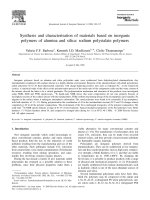
Figure 1.1.1: A giant burning ball of compressed hydrogen gas. The Sun is the primary
source of energy on Earth due to the fusion of hydrogen atoms in its core. Large masses
of hydrogen undergo fusion to form helium atoms, thereby releasing energy. Electro-
magnetic radiation from the sun reaches the earth as sunlight, and may be converted
into useful work by using sunlights heat, or converting the light into electricity. (Image
courtesy of NASA).
process can be represented as the conversion
4p
+
→
4
2
He +2e
+
+ 2ν
e
+ 2γ (1.1.2)
releasing photons or light energy (γ) into space, while four hydrogen (H) atoms are con-
verted into one helium (He) atom. The neutrino (ν
e
) energy flux released in the process
is about 10
11
cm
−2
s
−1
, or about 3% of the energy emitted compared to the photon (γ)
energy [35–37], and can be subtracted from the total energy emission. Equation 1.1.2
results in a net reduction of mass. The reduction in mass is due to the energy difference
between free hydrogen atoms and the bound helium core. Using the atomic mass units
(amu) for hydrogen and helium, and Avogadro’s constant (which is 6.022 × 10
23
mol
−1
)
the mass of hydrogen before fusion is 4 × 1.00794/6.022 × 10
23
, and the mass of helium
after fusion is 4.0026/6.022 × 10
23
.
Using the Einstein mass-energy relationship [38], the difference in mass is equated
3
to the energy emitted from the sun. Converting mass to kg, and dividing by time, the
power per fusion event emitted uniformly into 4π steradians surrounding the sun is
P =
E
t
=
(∆m) c
2
t
(1.1.3)
=
4 × 1.00794 − 4.0026
6.022 × 10
26
c
2
t
. (1.1.4)
Since H is consumed at approximately 620 × 10
9
kg/s [39], the total rate of mass
negated is 620 × 10
9
kg/s ×
4×1.00794
4.0026
− 1
= 4.516 × 10
9
kg/s and the power emitted
becomes
P = 4.516 × 10
9
kg/s ×(299792458 m/s)
2
= 4.05 × 10
28
W. (1.1.5)
At a distance of one astronomical unit from the sun (the distance from the sun to the
earth) the power incident on one square meter is thus
97%
4.05 × 10
28
4π (150 ×10
9
)
2
= 1391 W/m
2
. (1.1.6)
The factor of 97% subtracts the neutrino energy. This value corresponds closely with a
modern determination of the solar constant [40, 41] outside of the earths atmosphere,
being 2% higher than an accepted value of 1360.8 W/m
2
.
By multiplying the determined solar constant by the cross-section of the earth, the
total time t through which the solar insolation incident upon the earth’s atmosphere
equals the energy consumed by humankind in one year (see Equation 1.1.1) is
t =
474 × 10
18
(1435 W/m
2
)π (6387.1 km)
2
, (1.1.7)
which gives 2584 s, or roughly 43 minutes. Alternatively, matching humankind’s rate of
energy consumption to an equivalent area A of solar power gives
A =
474 × 10
18
J/1 yr.
(1435 W/m
2
)
= 10474 km
2
. (1.1.8)
This is approximately the size of Jamaica, Qatar, or the smallest sovereign state of
4
continental Africa, Gambia. Moreover, dividing the mass of the sun by the rate of mass
conversion, the remaining lifetime of the sun is on the order of 1.98892 ×10
30
kg/620 ×
10
9
kg/s ≈ 100 ×10
9
years, or at least billions of years
5
.
1.1.2 The solar spectrum
Figure 1.1.2: The radiation emitted from the sun is absorbed and scattered in the earth’s
atmosphere. The AM0 spectrum represents the sun’s radiation outside of the earth’s
atmosphere (red). The spectrum reaching ground level at earth is represented by the
AM1.5 spectrum (green and blue). It is this spectrum which must be converted to useful
energy to provide solar power. (Image adapted from PV-CDROM [45]).
Sunlight may be characterized by its spectrum to identify an appropriate material
that may convert the solar spectrum into useful energy, such as electricity. The surface
temperature of the sun is approximately 5778 K. Modeled as a black-body, the spectrum
of light emitted by the sun can be calculated using the Planck law which states
I (ω, T) =
4π¯hω
3
/c
2
e
¯hω/k
B
T
− 1
−1
. (1.1.9)
5
The assumption used here does not relate to modern astrophysical models of stellar evolution, which
may be found in the literature [42–44]. In any case, sunlight should be available for a long time, and
thus solar power is classified as a renewable energy.
5
I is the spectral radiance, ν is the electromagnetic frequency, T is the temperature of
the black-body, ¯h is the reduced Planck constant, c is the speed of light, and k
B
is the
Boltzmann constant.
The air mass (AM) of the atmosphere defined as AM = 1/ cos (θ), with θ measured
as an angle from overhead, defines the AM0 spectrum outside the earth’s atmosphere,
and the AM1.5 spectrum representing the irradiation of the sun at the earth’s surface
(θ = 48
◦
) (see Fig. 1.1.2). As the air mass increases, the attenuation of light shifts
the spectrum to the red, since scattering of light increases with the photon energy by
≈ ω
4
. This explains why the sky is blue, while a sunset appears orange. The AM spectra
[46, 47] as the radiative power at earth is written I
AM
. The Standard Tables for
Reference Solar Spectral Irradiances give a value of the integral of the spectrum
as 888 W/m
2
for terrestrial applications [47]. Average values for solar insolation can be
obtained from NASA [48], for example, or the National Renewable Energy Laboratory
(NREL) [49].
The conversion of sunlight into useful work is a candidate for renewable energy since
sunlight is abundant, and sufficiently dense in energy. Sunlight can provide humankind
with considerable amounts of solar generated power, if the energy can be converted or
stored efficiently. The conversion of sunlight into work using heat is known as solar-
thermal energy [50–52]. Heat can be used to drive a turbine, or heat water [53]. Below,
the photovoltaic effect and silicon-based devices used to exploit the photovoltaic effect
are introduced, followed by luminescence-based characterization of these devices.
1.1.3 The photovoltaic effect for direct conversion of sunlight into electricity
The direct conversion of sunlight into electricity uses the photovoltaic effect [54–56]. The
focus of the present work is on the characterization of silicon-based devices designed to
enable photovoltaic energy conversion of sunlight energy into electricity. For more infor-
mation on photovoltaic energy conversion, solar cell physics, and design architectures,
the reader is referred to the literature [28, 31, 57–65].
Solar electric energy generation using the photovoltaic effect may be enabled using
6
Figure 1.1.3: The photovoltaic effect at a pn junction showing the formation of an
electron and hole due to the absorption of a photon of energy ¯hω. The bulk is p-
type, while the emitter is n-type. The majority of the base region is quasi-neutral with
respect to the electric potential, and diffusion of the photo-generated minority carriers
dominates. Some minority carriers (electrons in the case of a p-type base) diffuse towards
the depletion region and are influenced by the electric field close to the pn junction. The
electric field formed at the junction region drives the excess charge carriers so that
the electrons will flow in only one direction. The generation of an electric field at the
depletion region establishes a voltage on the device, while the flow of charges establishes
a current. The current and voltage together establish the output power of the device.
an electronic device called a solar cell [66–68]. Figure 1.1.3 shows a cross-section of
a solar cell. The photovoltaic effect was discovered in 1839 by Alexandre Edmond
Becquerel [54]. Becquerel noticed that certain metal/electrolyte systems provided
electrical currents upon incidence of light [54, 55]. This effect is due to the liberation
of electrons upon absorption (annihilation) of photons. A combination of the diffusion
of liberated electrons (holes) and forces on these charge carriers by the electric fields
in the material causes charge carriers to flow, producing a net current and a voltage at
the device terminals [56, 62, 69]. Modern solar cells use semiconductors, not electrolyte
solutions
6
, to harness the photovoltaic effect. Silicon-based technologies dominate the
market [58, 70].
When sunlight is incident on a solar cell, the energy is transferred to electrons bound
in the material [71, Chapter 8, p. 195]. Electrons will go from a lower energy state called
the valence band, into a higher energy state called the conduction band, leaving behind
a positive charge in the valence band, known as a hole. The minimum photon energy
6
With the exception of organic solar cells.
7
Figure 1.1.4: The I-V curve (a) and simple diode model of a solar cell (b), demonstrate
the operation of a solar cell. The power curve in blue calculated by P = V I shows
a maximum for a particular current and voltage. In (b) the simple diode is based on
parameters I
L
, the current generated at the source when the device is illuminated, and
I
0
, the saturation current.
required to excite the electron into the conduction band is known as the bandgap energy.
The liberated electrons and holes are able to move around the material [72, Chapter 2,
p. 27]. The result of the annihilation of light energy is the creation of two charges in the
solar cell, one negative and another positive.
Inside the solar cell different layers of material are created through a process called
doping or diffusion [73]. The solar cell shown in Figure 1.1.3 has two regions, a base
fabricated with an excess of free positive charge carriers, and an emitter with an excess of
free negative charge carriers. The boundary of these regions forms a pn junction [68, 69,
74] resulting in an electric field that causes charge carriers to drift. The physics of the pn
junction is described in detail in sources such as the book by Sze [65, Chapter 2,p. 79-
133] or Luque, et al. [28, Section 3.2.8,p. 102]. Due to drift and diffusion, a net
current flow is achieved in the device upon illumination. The result is that light energy
is converted into a flow of electrons which may power a connected load.
The photovoltaic conversion efficiency η
P V
can be written as the division of the
electrical energy by the sunlight energy as
η
P V
=
V
mpp
I
mpp
I
AM
(λ) dλ
(1.1.10)
where V
mpp
is the voltage and I
mpp
is the current at the maximum power point of the
8
solar cell. I
AM
represents the optical power incident at ground level (see Figure 1.1.2).
The denominator integrates to a constant value which depends on the location of the
photovoltaic system, as well as meteorological conditions, or the module inclination. A
standard solar cell I-V curve is shown in Figure 1.1.4, together with the power-voltage
curve. The solar cell must operate at a particular point on the curve. The output power
peaks at the maximum power point. Optimization of this electrical energy generation
process in an economical manner is the key aspect of silicon wafer-based photovoltaic
research and engineering [75, 76]. For example, selective emitters, back surface fields,
and specific chemical processing procedures for passivation and texturing of silicon wafer
solar cells have been developed [58]. More details on the fabrication of silicon wafer solar
cells may be found in the Handbook of Photovoltaic Science and Engineering
by Luque, et al [28], and other books [59, 77].
1.1.4 Generation of electrons and holes
The generation of an electron and hole in a semiconductor may occur upon the absorp-
tion of a photon of energy E
γ
= ¯hω. The process of absorption at room temperature
may include the addition of a phonon of vibrational energy, along with the absorption of
light energy. This allows momentum and energy conservation for excitation of an elec-
tron into the conduction band of an indirect semiconductor. Energy transitions in the
semiconductor may also involve localized states in the bandgap [62]. Such transitions
involve only a single electron or hole. Photovoltaic conversion requires the generation
and collection of both an electron and hole to provide a net current from the device.
In steady-state, the Poisson equation and continuity equations govern the concen-
tration of charges in the semiconductor [65, 71, 78, 79]. These equations are
∇ ·
E = q (p − n + N) , (1.1.11)
∇ ·
J
p
= q
G − R
p
−
∂p
∂t
, (1.1.12)
∇ ·
J
n
= q
R
n
− G +
∂n
∂t
, (1.1.13)
9
Figure 1.1.5: (a) Estimated annual growth figures of solar markets by country. The
compounded annual growth rate of the solar energy market from 2000 to 2009 is esti-
mated at 39%. (b) Technologies leading the solar energy market. Wafer-based silicon
technologies currently dominate the solar market.
respectively. This includes the concentrations of the free electrons n and free holes
p, while N may be written N = N
+
D
− N
−
A
+ N
+
T
, q is the electron charge, and the
electric field is
E. N
+
T
is the net recombination due to defects in the bulk of the solar
cell. The current density vectors for electrons and holes are
J
n
and
J
p
, respectively.
The rates of change in the electron and hole concentrations
∂n/p
∂t
are constrained by the
terms G for the optical generation rate of electron-hole pairs, and R
n/p
accounting for
recombination. The generation rate G is proportional to G(z) = αj
γ
(z) at a distance of
z into the material, where j
γ
is the particle flux of photons transmitted into the silicon
material, and α is the absorption coefficient. These general equations constrain the
rates of change of charge concentration in the material, and may be used to compute
the electrical performance of a device based on its specific boundary conditions.
1.1.5 Silicon-wafer photovoltaic devices
Silicon wafer technologies currently dominate the market (see Fig. 1.1.5). This Thesis
focuses on characterization of silicon wafer-based photovoltaic devices. A silicon wafer
solar cell is fabricated in a series of processing sequences whereby the raw silicon is
grown, sliced into wafers, doped to create a junction, and finally optically coated and
metalized [28, 80].
A procedure for fabricating a silicon wafer solar cell is shown in Figure 1.1.6. The
10