Characterization and design of CMOS components for microwave and millimeter wave applications
Bạn đang xem bản rút gọn của tài liệu. Xem và tải ngay bản đầy đủ của tài liệu tại đây (4.76 MB, 149 trang )
CHARACTERIZATION AND DESIGN OF CMOS COMPONENTS
FOR MICROWAVE AND MILLIMETER WAVE APPLICATIONS
NAN LAN
(B.S., Nanjing University, China)
A THESIS SUBMITTED
FOR THE DEGREE OF DOCTOR OF PHILOSOPHY
DEPARTMENT OF ELECTRICAL AND COMPUTER ENGINEERING
NATIONAL UNIVERSITY OF SINGAPORE
2009
ACKNOWLEDGEMENTS
The work described in this thesis could not have been accomplished without
the help and support of many individuals.
I owe my deepest gratitude to my supervisor Assistant Professor Koen Mouthaan,
who fueled my interest in this field of research when I was an undergraduate stu-
dent, and offered me the opportunity to advance my study for a PhD degree. His
knowledge and passion in the related research fields have led me to discover the
challenging problems in industry and encour aged me to explore theoretical and
practical solutions. Throughout more than four years, he has guided me along in
weekly meetings and helped me to overcome difficulties whenever I got stuck. I
have also benefited from his training in other asp ects, such as analytical thinking,
English language, building self-confidence in pu blic presentations, and so on. All
of this has been beneficial b oth to my academic progress and personal growth.
I sincerely appreciate my co-supervisor Dr. Yong-Zhong Xiong from the Insti-
tute of Microelectronics, Singapore. I would like to thank him for his constructive
advice in my research progress, and for providing important resources, especially
the devices in the cutting-edge technology at that time and the measurements for
noise characterization.
My gratitude is extended to the late Associate Professor Ban-Leong Ooi, who
was also my co-supervisor. I learned a lot from him, and many ideas were sparked
through discussions with him. Those experiences are my cherished memories.
I am grateful to Dr. Subhash Chander Rustagi for his support in the TSRP
project on the modeling of CMOS passives.
ii
I am thankful to all the friends who h elped me in my study and life in Singapore.
I am fortunate to have worked with the members in the MMIC Packaging and
Modeling Lab of National University of Singapore in a stimulating and enjoyable
research environment. The friendship with themhas been invaluable to me.
I appreciate the friendly interactions with staff from the Integrated Circuit
and System Lab in the Institute of Microelectronics, Singapore. Many useful
discussions with them as well as t echnical support in the measurements have been
of great benefit to my research work.
Special thanks to my boyfriend for bringing me so much joy and for his ever-
lasting patience.
Last but not the least, I wish to thank my parents for bringing me up and for
their forever love. I have always been learning to be more kind-hearted, patient,
and optimistic from them.
iii
TABLE OF CONTENTS
Chapter 1 : Introduction 1
1.1 CMOS Technology for Microwave and Millimeter Wave Applications 1
1.2 CMOS Components . . . . . . . . . . . . . . . . . . . . . . . . . . . 3
1.2.1 MOSFETs . . . . . . . . . . . . . . . . . . . . . . . . . . . . 3
1.2.2 Passive Components . . . . . . . . . . . . . . . . . . . . . . 5
1.3 Motivation, Scope, and Thesis Organization . . . . . . . . . . . . . 7
1.4 List of Publications . . . . . . . . . . . . . . . . . . . . . . . . . . . 9
Chapter 2 : On-Wafer Measurements and De-embedding 12
2.1 Introduction . . . . . . . . . . . . . . . . . . . . . . . . . . . . . . . 12
2.2 S-Parameter Measurements . . . . . . . . . . . . . . . . . . . . . . 12
2.2.1 S-Parameters . . . . . . . . . . . . . . . . . . . . . . . . . . 12
2.2.2 Vector Network Analyzer . . . . . . . . . . . . . . . . . . . . 13
2.3 Noise Parameter Measurements . . . . . . . . . . . . . . . . . . . . 15
2.4 De-embedding Techniques . . . . . . . . . . . . . . . . . . . . . . . 17
2.4.1 Pad De-embedding . . . . . . . . . . . . . . . . . . . . . . . 18
2.4.2 “Thru” De-embedding . . . . . . . . . . . . . . . . . . . . . 19
2.4.3 “Open-Short” De-embedding . . . . . . . . . . . . . . . . . . 21
2.4.4 Three-Step De-embedding . . . . . . . . . . . . . . . . . . . 23
2.4.5 “Thru-Short” De-embedding . . . . . . . . . . . . . . . . . . 25
2.5 Results and Discussions . . . . . . . . . . . . . . . . . . . . . . . . 26
iv
2.5.1 Case 1: S-Parameter De-embedding for Two-Port Transmis-
sion Lines . . . . . . . . . . . . . . . . . . . . . . . . . . . . 26
2.5.2 Case 2: S-Parameter De-embedding for Source Grounded
Transistors . . . . . . . . . . . . . . . . . . . . . . . . . . . . 28
2.5.3 Case 3: Noise Parameter De-embedding for Source Grounded
Transistors . . . . . . . . . . . . . . . . . . . . . . . . . . . . 30
2.6 Conclusions and Recommendations . . . . . . . . . . . . . . . . . . 34
Chapter 3 : Microwave Noise Characterization of MOSFETs 35
3.1 Introduction . . . . . . . . . . . . . . . . . . . . . . . . . . . . . . . 35
3.2 Methodology . . . . . . . . . . . . . . . . . . . . . . . . . . . . . . 36
3.3 Small Signal Parameter Extraction . . . . . . . . . . . . . . . . . . 39
3.3.1 Terminal Resistances . . . . . . . . . . . . . . . . . . . . . . 40
3.3.2 Intrinsic Parameters . . . . . . . . . . . . . . . . . . . . . . 41
3.3.3 Drain Substrate Parameters . . . . . . . . . . . . . . . . . . 44
3.3.4 Optimization . . . . . . . . . . . . . . . . . . . . . . . . . . 45
3.3.5 Experimental Results . . . . . . . . . . . . . . . . . . . . . . 45
3.4 Noise Source Extraction . . . . . . . . . . . . . . . . . . . . . . . . 49
3.4.1 Substrate Network Transformation . . . . . . . . . . . . . . 50
3.4.2 Noise Source De-embedding and Contribution Breakdown . . 52
3.5 Noise Source Distribution . . . . . . . . . . . . . . . . . . . . . . . 56
3.6 Intrinsic Noise Source Modeling . . . . . . . . . . . . . . . . . . . . 56
3.6.1 Drain Current Noise . . . . . . . . . . . . . . . . . . . . . . 57
3.6.2 Gate Current Noise . . . . . . . . . . . . . . . . . . . . . . . 60
3.7 Scaling of Minimum Noise Figure . . . . . . . . . . . . . . . . . . . 64
3.7.1 Intrinsic Noise . . . . . . . . . . . . . . . . . . . . . . . . . . 65
3.7.2 Extrinsic Noise . . . . . . . . . . . . . . . . . . . . . . . . . 67
3.8 Conclusions and Recommendations . . . . . . . . . . . . . . . . . . 68
v
Chapter 4 : Modeling of Inductors with Metal Dummy Fills 69
4.1 Introduction . . . . . . . . . . . . . . . . . . . . . . . . . . . . . . . 69
4.2 Design and Measurement of Inductor Counterparts . . . . . . . . . 70
4.2.1 Design of Experiment . . . . . . . . . . . . . . . . . . . . . . 70
4.2.2 Fabrication and Measurement . . . . . . . . . . . . . . . . . 72
4.3 Modeling of Inductors . . . . . . . . . . . . . . . . . . . . . . . . . 72
4.4 Effect of Metal Dummy Fills On Inductors . . . . . . . . . . . . . . 76
4.5 Model Modification . . . . . . . . . . . . . . . . . . . . . . . . . . . 77
4.5.1 Method 1: Parallel-Plate Assumption . . . . . . . . . . . . . 81
4.5.2 Method 2: Fringing Field Consideration . . . . . . . . . . . 82
4.5.3 Update of the Compact Model . . . . . . . . . . . . . . . . . 83
4.6 Conclusions and Recommendations . . . . . . . . . . . . . . . . . . 85
Chapter 5 : Millimeter Wave Thin Film Microstrip Lines in CMOS 86
5.1 Introduction . . . . . . . . . . . . . . . . . . . . . . . . . . . . . . . 86
5.2 TFMS Structure . . . . . . . . . . . . . . . . . . . . . . . . . . . . 88
5.3 Unloaded Q-factor . . . . . . . . . . . . . . . . . . . . . . . . . . . 90
5.4 Experiment of TFMS Lines . . . . . . . . . . . . . . . . . . . . . . 92
5.4.1 Fabrication and Measurement . . . . . . . . . . . . . . . . . 92
5.4.2 Results . . . . . . . . . . . . . . . . . . . . . . . . . . . . . . 93
5.5 Conclusions and Recommendations . . . . . . . . . . . . . . . . . . 97
Chapter 6 : Millimeter Wave Filters in 0.18-µm CMOS 98
6.1 Introduction . . . . . . . . . . . . . . . . . . . . . . . . . . . . . . . 98
6.2 Narrow Bandpass Filters . . . . . . . . . . . . . . . . . . . . . . . . 99
6.2.1 Designed Structures . . . . . . . . . . . . . . . . . . . . . . 102
6.2.2 Results . . . . . . . . . . . . . . . . . . . . . . . . . . . . . . 102
6.2.3 Loss Analysis . . . . . . . . . . . . . . . . . . . . . . . . . . 103
vi
6.3 Bandpass Filters with Small to Moderate Bandwidths . . . . . . . . 108
6.4 Conclusions and Recommendations . . . . . . . . . . . . . . . . . . 111
Chapter 7 : Conclusions and Recommendations 113
7.1 Measurements and De-embedding . . . . . . . . . . . . . . . . . . . 114
7.2 Microwave Noise Modeling of MOSFETs . . . . . . . . . . . . . . . 116
7.3 Effects of Metal Dummy Fills . . . . . . . . . . . . . . . . . . . . . 117
7.4 Millimeter Wave Filters . . . . . . . . . . . . . . . . . . . . . . . . . 119
vii
Summary
Accurate models of the on-chip active and passive components are essential for
successful CMOS IC designs. This work aims to characterize important active and
passive components in modern CMOS technologies for microwave and millimeter
wave applications to accommodate the two trends in many practical applications:
smaller technology nodes and higher operating frequencies. The thesis is mainly
concerned with the noise characterization of 65nm RF n-MOSFETs, modeling of
the impact of metal dummy fills on the microwave behavior of spiral inductors,
and the design of line resonators and filters at 60 GHz and 77 GHz in a 0.18-µm
CMOS process.
To investigate the noise properties of the nano-scale MOSFETs at microwave fre-
quencies, the various noise sources in the MOSFETs are extracted based on an
equivalent circuit from measured S-parameters and noise parameters. It is found
that the intrinsic noise figure generally improves with a shorter gate length, mainly
due to the reduced induced gate noise. However, the excess noise increases in the
shorter channels which holds back the improvement of the intrinsic noise figure
of the MOS FETs to a certain extent. Additionally, the thermal noise from the
extrinsic parasitics, particularly the gate resistance which is inversely proportional
to the gate length, has an increasing weight in the total MOSFET noise figure.
The overall noise performance may deteriorate when the gate length reduces to
below 100 nm.
In smaller CMOS technology nodes, metal dummy fills are inserted in all the met-
allization layers to fulfill the process metal density and uniformity requirements.
They influence the passive components when the frequency increases into the mi-
viii
crowave range. The Q-factor of the on-chip spiral inductors is shown to be degraded
by the inserted metal dummy fills. By comparing the extracted model parameters
based on a physics-based mo del from the experimental results, it is found that the
main reason for the reduced Q-factor is due to the increased oxide capacitance.
A methodology is proposed to update existing inductor models by modifying the
oxide capacitance analytically.
The feasibility of implementing millimeter wave passive filters in standard CMOS
technology is studied in this thesis. A technique to use the lowest metallization as
a ground plane is exploited to reduce the losses in the silicon substrate. First, the
best layer configuration for transmission lines with the ground plane in a 0.18-µm
CMOS is identified by comparing the unloaded Q-factors of three viable options.
Next, coupled-line bandpass filters at 60 and 77 GHz with different bandwidths are
realized using λ/4 line resonators. The relationship between the center frequency
insertion loss and the 3-dB bandwidth is determined experimentally. The results
provide trade-off considerations for the design of the 60 GHz and 77 GHz filters in
CMOS.
ix
LIST OF TABLES
3.1 Model Parameters of MOSFET L60 with V
D
= 0.6 V and I
D
= 1 mA 49
4.1 Design Parameters for Inductors . . . . . . . . . . . . . . . . . . . . 71
4.2 Extracted Parameter Values and Changes for Inductors with and
without Metal Dummy Fills (W =6 µm) . . . . . . . . . . . . . . . 78
4.3 Extracted Parameter Values and Changes for Inductors with and
without Metal Dummy Fills (W =10 µm) . . . . . . . . . . . . . . . 79
6.1 Design Parameters for Inductors . . . . . . . . . . . . . . . . . . . . 102
6.2 Performance Comparison of Previously Published Narrow Bandpass
Filters and This Work . . . . . . . . . . . . . . . . . . . . . . . . . 107
6.3 Design and layout parameters for the filters with various 0.5-dB FBWs109
x
LIST OF FIGURES
1.1 Frequency spectrum of wireless applications (after [1]). . . . . . . . 1
1.2 Predicted scaling of the gate length and peak f
max
and peak f
T
of
CMOS technology in near- and long-term (after [1]). . . . . . . . . . 3
2.1 Block diagram of a vector network analyzer (VNA). . . . . . . . . . 14
2.2 System setup for S-parameter and noise and on-wafer measurements. 16
2.3 Layout of the test structure of the DUT. The measurement reference
planes are located at the probe tips after calibration. . . . . . . . . 17
2.4 (a) Layout of an “open” standard. (b) The parasitic model of the
DUT test-structure in a pad de-embedding method . . . . . . . . . . 18
2.5 (a) Layout of the DUT test-structure. (b) Layout of a “thru” stan-
dard. (c) The parasitic model of the DUT test-structure in a “thru”
de-embedding method. . . . . . . . . . . . . . . . . . . . . . . . . . 20
2.6 The parasitic model of the DUT test-structure in an improved “thru”
de-embedding method. . . . . . . . . . . . . . . . . . . . . . . . . . 20
2.7 (a) Layout of a DUT containing a tr ansistor with the source con-
nected to ground bars. (b) Layout of the “short” standard. . . . . . 22
2.8 The parasitic model of the DUT test-structure (a) in an “open-
short” de-embedding scheme and (b) in a “short-open ” scheme. . . 22
2.9 Layout of (a) “open”, (b) “thru”, (c) “short1”, and (d) “short2”. . . 23
2.10 The parasitic model of the DUT test-structure in a three-step de-
embedding method. . . . . . . . . . . . . . . . . . . . . . . . . . . . 24
xi
2.11 The parasitic mo del of the DUT test-structure in a “thru-short”
de-embedding method. . . . . . . . . . . . . . . . . . . . . . . . . . 25
2.12 The structure of the transmission lines fabricated in a 0.18-µm
CMOS technology. . . . . . . . . . . . . . . . . . . . . . . . . . . . 26
2.13 De-embedded S-parameters for a 800 µm long an d 10 µm wide trans-
mission line using different de-embedding methods. Momentum EM
simulation results are also shown. . . . . . . . . . . . . . . . . . . . 27
2.14 De-embedded S- parameters for a 16-finger MOSFET with V
G
= 0.7
V and V
D
= 1.8 V using different de-embedding metho d s. . . . . . . 29
2.15 Extracted R
s
and L
s
of the source ground legs in the “short”. . . . 31
2.16 Measured and de-embedded noise-parameters for a 0.18-µm MOS-
FET with a total width of 80 µm biased at V
ds
= 1.8 V and V
gs
=
0.7 V. (a) Minimum noise figure, (b) noise resistance, (c) magnitude
of optimized source reflection coefficient, and (d) ph ase of optimized
source reflection coefficient. . . . . . . . . . . . . . . . . . . . . . . 33
3.1 Cross-sectional view of a gate finger in a MOSFET with equivalent
circuit elements. . . . . . . . . . . . . . . . . . . . . . . . . . . . . . 36
3.2 MOSFET Microwave noise model. . . . . . . . . . . . . . . . . . . . 37
3.3 Extraction flow for the MOSFET small signal equivalent circuit
shown in Figure 3.2. . . . . . . . . . . . . . . . . . . . . . . . . . . 40
3.4 MOSFET small signal equivalent model at DC or low frequencies. . 42
3.5 Small signal equivalent model of an intrinsic MOSFET. . . . . . . . 42
3.6 Substrate network of the small-signal equivalent circuit as shown in
Figure 3.2. . . . . . . . . . . . . . . . . . . . . . . . . . . . . . . . . 44
3.7 Logarithm of I
D
in mA against V
G
. Symbols are measured data. . . 46
xii
3.8 Curve fitting for estimating the terminal resistances. (a) To estimate
R
g
, R
d
, and R
s
for L60 with V
D
= 1.2 V and I
D
= 1 mA. (b) To
estimate R
g
for the four MOSFETs. The scattered symbols are
measurements up to 18.5 GHz, and the lines are the fitted curves
calculated up to 100 GHz to show the values. . . . . . . . . . . . . 47
3.9 Extraction of (a) g
m
, (b) R
ds
, (c) C
gd
, and (d) C
gg
for L60 with V
D
= 1.2 V and I
D
= 1 mA. . . . . . . . . . . . . . . . . . . . . . . . . 48
3.10 Comparison of measured and modeled S-parameters for L60 with
V
D
= 0.6 V and I
D
= 1 mA. . . . . . . . . . . . . . . . . . . . . . . 50
3.11 Small-signal model parameters for the MOSFETs. . . . . . . . . . . 51
3.12 Cutoff frequency of the measured MOSFETs. . . . . . . . . . . . . 52
3.13 Substrate network tran sformation for intrinsic noise sour ce extrac-
tion. (a)-(d) network transformantion steps. (e) final equivalent
circuit. . . . . . . . . . . . . . . . . . . . . . . . . . . . . . . . . . . 53
3.14 Equivalent noise circuit representation of the intrinsic MOSFET. . . 55
3.15 The contribution of the various noise sources in the excess noise
factor (F
min
− 1) of the MOSFETs with I
D
= 0.6V and I
D
= 1mA. 56
3.16 Drain noise power spectral density S
id
for L60 from measurements.
Full symbols are with a low drain voltage of 0.6 V, and empty sym-
bols are with a higher voltage of 1.2 V. . . . . . . . . . . . . . . . . 59
3.17 Extracted drain n oise power spectral density S
id
at 14 GHz against
the DC drain current. The drain voltage is 0.6 V. Theoretical calcu-
lations of shot noise (2qI
D
) and thermal noise (8kT g
m
/3) are shown
for comparison. . . . . . . . . . . . . . . . . . . . . . . . . . . . . . 61
3.18 Drain noise power spectral density S
id
of L60 with V
D
= 0.6 V and
I
D
= 1 mA. Symbols are measured data. Modeled flicker noise,
thermal noise, and the sum of them are also shown. . . . . . . . . . 62
xiii
3.19 Symbols: extracted gate current noise power spectral density S
ig
for
the MOSFETs with I
D
= 1 mA. Lines: modeled gate current noise
taking into account the gate tunneling noise and the induced gate
noise. . . . . . . . . . . . . . . . . . . . . . . . . . . . . . . . . . . . 63
3.20 Extracted correlation coefficient for the MOSFETs with different
drain currents. . . . . . . . . . . . . . . . . . . . . . . . . . . . . . . 64
3.21 Simplified noise model for the MOSFET with three noise sources:S
id
,
S
ig
and R
g
. . . . . . . . . . . . . . . . . . . . . . . . . . . . . . . . 64
3.22 γ and β factors versus gate length with V
D
= 0.6 V and I
D
= 1 mA. 65
3.23 Calculated NF
min,int
with varying γ and β for L60 with V
D
= 0.6 V
and I
D
= 1 mA. . . . . . . . . . . . . . . . . . . . . . . . . . . . . . 66
3.24 Intrinsic NF
min
against gate length L with V
D
= 0.6 V and I
D
= 1
mA. . . . . . . . . . . . . . . . . . . . . . . . . . . . . . . . . . . . 67
3.25 Measured NF
min
against gate length L with V
D
= 0.6 V and I
D
=
1 mA. . . . . . . . . . . . . . . . . . . . . . . . . . . . . . . . . . . 68
4.1 The experimental set including 14 pairs of inductors and 4 “thru”
standards. . . . . . . . . . . . . . . . . . . . . . . . . . . . . . . . . 71
4.2 Microphotographs of fabricated inductors with W =6 µm, S=6 µm,
ID=78 µm, and N=3.5 (a) without metal dummy fills, and (b) with
metal dummy fills. (c) Regional enlarged view of (b). . . . . . . . . 72
4.3 The equivalent single π-model for on-ship spiral inductors. . . . . . 73
4.4 Measured (a) inductance, (b) resistance, (c) oxide capacitance, and
(d) substrate capacitance for inductors with W=6 µm, S=2 µm,
ID=70 µm, and N=3.5 with and without metal dummy fills. . . . . 75
4.5 Comparison of the measured and simulated Q-factors of inductor
with W=6 µm, S=2 µm, ID=70 µm, and N=3.5 with and without
metal dummy fills. . . . . . . . . . . . . . . . . . . . . . . . . . . . 76
xiv
4.6 Change in Q
max
versus the changes in (a) C
ox
, (b) C
sub
, and (c) R
sub
for the inductor with W =6 µm, S=2 µm, ID=70 µm, and N=3.5. . 80
4.7 (a) 3-D view of the spiral inductor with metal dummy fills. (b) Top
view. (c) Cross-sectional view of the inserted metal dummies in M1
to M5. . . . . . . . . . . . . . . . . . . . . . . . . . . . . . . . . . . 81
4.8 Comparison of the measured, simulated and predicted Q-factors of
inductor with metal dummy fills with W =6 µm, S=2 µm, ID=70
µm, N=3.5 using two methods. . . . . . . . . . . . . . . . . . . . . 84
4.9 Predicted Q
max
versus measured Q
max
by updating C
ox
using two
methods. . . . . . . . . . . . . . . . . . . . . . . . . . . . . . . . . . 84
4.10 Predicted f
max
versus measured f
max
by updating C
ox
using two
methods. . . . . . . . . . . . . . . . . . . . . . . . . . . . . . . . . . 85
5.1 Illustration of parallel-coupled resonator filters using CPW lines. . . 87
5.2 Layer configuration in a 0.18-µm CMOS process. . . . . . . . . . . 89
5.3 Configurations of TFMS lines: (a) TFMS-M6. (b) TFMS-M5. (c)
TFMS-M56. . . . . . . . . . . . . . . . . . . . . . . . . . . . . . . . 89
5.4 λ
0
/4 line resonators and equivalent circuits. (a) Open-circuited and
(b) short-circuited. . . . . . . . . . . . . . . . . . . . . . . . . . . . 91
5.5 Fabricated TFMS lines. . . . . . . . . . . . . . . . . . . . . . . . . . 93
5.6 Extracted α and β for a TFMS-M6 line with W=12 µm, L=670 µm. 94
5.7 (a) Examination the condition of small loss. (b) Determination of
the resonance frequency f
0
for the λ/4 line where βL/π = 0.5 for a
TFMS-M6 line with W = 12 µm, L = 670 µm. . . . . . . . . . . . 94
5.8 (a) Extracted Q
u
and (b) Magnitude of the characteristic impedance
|Z
0
| for a TFMS-M6 line with W =12 µm, L=670 µm. . . . . . . . . 95
5.9 Comparison of simulated and measured Q
u
of TFMS-M6 lines. . . . 95
xv
5.10 Comparison of measured Q
u
of TFMS lines resonators at th e reso-
nance frequency. . . . . . . . . . . . . . . . . . . . . . . . . . . . . . 96
5.11 Measured Q
u
of TFMS-M6 and TFMS-M5 line resonators against
the line width at 60 GHz. . . . . . . . . . . . . . . . . . . . . . . . 97
6.1 Block diagram of the millimeter-wave front-end of an automotive
radar system. . . . . . . . . . . . . . . . . . . . . . . . . . . . . . . 98
6.2 Structures of even- and odd-mode coupled lines simulated in Sonnet
EM. . . . . . . . . . . . . . . . . . . . . . . . . . . . . . . . . . . . 101
6.3 Transformation map between even-mode and odd-mode characteris-
tic impedances (Z
0e
and Z
0o
) and layout parameters (width W and
spacing S). . . . . . . . . . . . . . . . . . . . . . . . . . . . . . . . 101
6.4 Micrographs of the designed filters with a target fractional band-
width of 5% at center frequencies of (a) 60 GHz and (b) 77 GHz. . 102
6.5 Measured and de-embedded data compared with simulation results
using Sonnet EM and Agilent’s Momentum for th e 60-GHz bandpass
filter. (a) Return loss. (b) Insertion loss. . . . . . . . . . . . . . . . 103
6.6 Measured and de-embedded data compared with simulation results
using Sonnet EM and Agilent’s Momentum for th e 77-GHz bandpass
filter. (a) Return loss. (b) Insertion loss. . . . . . . . . . . . . . . . 104
6.7 Loss analysis. (a) Non-dissipative filter. (b) Filter with lossy SiO
2
dielectric layer included. (c) Filter with lossy conductors in M6
included. (d) Filter with lossy ground plane in M1 and ideal silicon
substrate. (e) Actual filter. . . . . . . . . . . . . . . . . . . . . . . . 105
6.8 Simulated insertion losses of the five configurations in Fig. 6.7. . . . 106
6.9 Insertion loss versus 3-dB bandwidth for reported millimeter-wave
narrow bandpass filters in different technologies [75, 78-85]. . . . . . 108
xvi
6.10 Measured and simulated responses of filters with target FBWs of
10% to 40% at 60 GHz. . . . . . . . . . . . . . . . . . . . . . . . . . 110
6.11 Insertion loss against 3-dB bandwidth for filters at 60 GHz. The
theoretical relationship by Cohn’s formula is shown. Measured data
is compared with the performance of filters reported in [72, 86, 87]. 111
xvii
CHAPTER 1
Introduction
1.1 CMOS Technology for Microwave and Millimeter Wave
Applications
The rapid development and expansion of the wireless communication market has
driven the wide application of radio-frequency integrated circuits (RFICs). The
spectrum for most wireless applications is from the RF range to the millimeter
wave range allocated as illustrated in Fig. 1.1.
GSM
ISM
CDMA
0.8 GHz
WLAN
Bluetooth
802.1b/g
2.4 GHz
WLAN
802.1a
5 GHz
WLAN
UWB
10 GHz
WLAN
LMDS
28 GHz
Unlisenced
short-
range
wireless
comm.
60 GHz
ACR
77 GHz 94 GHz
ACC
30 cm 3 mm3 cm
Frequency
Wavelength
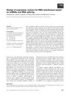
Figure 1.1: Frequency spectrum of wireless applications (after [1]).
With the growing interest in short-range broadband wireless communications
in microwave and millimeter wave frequency bands, such as 22-29 GHz and 76-77
GHz for automotive radar, and 57-64 GHz for unlicensed use, for higher data rates
of 100 Mbit/s to 1 Gbit/s and beyond, higher operating speeds or frequencies and
lower power consumption have been become general trends for wireless electronics
[2]. Advances in the semiconductor technologies for the microwave and millimeter
wave ICs are highly needed to fulfill these demands.
1
Traditionally, microwave ICs were mostly realized in III-V technologies. GaAs
or InP based field-effect transistors (MESFETs) and heterostructure field-effect
transistor (HFETs) can operate at higher speeds and are superior in low noise per-
formance because of the high mobility of the electrons. However, these technologies
are costly for consumer electronics.
Silicon-based technologies have received profound interest for reasons of low
cost and high yield. Between CMOS and SiGe BiCMOS technologies, CMOS
is even cheaper, and more advantageous in integrating digital circuits and data
storage devices on the same chip. A constant effort has been made to realize whole
communication systems on a single chip to further bring down the manufacturing
cost, complexity, and to improve the reliability. To this end, the integration of the
RF front-end circuits in CMOS is of key importance.
Fortunately, CMOS technology is being pushed to higher operating frequencies,
entering the millimeter wave range. MOSFETs with increased cutoff frequency f
T
around 200 GHz have now been realized due to the downscaling of the modern
CMOS technologies to the nano-scale level.
This downscaling phenomenon was first predicted by Gordon Moore in 1965:
the number of transistors on an IC would dou ble about every two years since
invention [3]. This infers a scaling factor of
√
2 of the feature size designated by the
“DRAM half-pitch” [4]. The semiconductor industry has almost kept the pace for
more than 40 years. Currently in year 2009, a 32nm logical CMOS technology has
been delivered by Intel on-target [5]. The scaling of CMOS technology generations
in near- and long-term predicted by the International Technology Roadmap for
Semiconductors (ITRS) is shown in Fig. 1.2 [1]. Note that, the smallest gate
length is generally smaller than the feature size of a technology generation. For
example, a 65nm CMOS can have a gate length smaller than 65 nm. Also shown in
Fig. 1.2 are the increase in the peak f
max
and peak f
T
of the MOSFETs resulting
2
from the downscaling [1]. Many high-speed and microwave ICs are likely to be
implemented in CMOS technology [6–10].
Figure 1.2: Predicted scaling of the gate length and peak f
max
and peak f
T
of
CMOS technology in near- and long-term (after [1]).
1.2 CMOS Components
The success in CMOS RFIC design strongly depends on the availability of accurate
models of the constituent components. New challenges are faced as the components
shrink in size, and operate at higher frequencies.
1.2.1 MOSFETs
The evolution of CMOS technologies has mostly been digital-oriented. The foundries
first develop the process for digital design which mainly targets higher transistor
density, higher speed, and lower power dissipation. Then, modifications may be
made to the process to suit mixed-signal and analog RF applications. Options such
as using copper in the top metal layer, thickening the top metal layer or adding
3
a special device mask may be taken. Moreover, the performance of the MOSFET
remains the foremost component to represent the progress of the process.
In terms of MOSFET application for RF circuits, there are three most impor-
tant figure-of-merit parameters: the cutoff frequency associated with the short-
circuit current gain f
T
, the maximum frequency of oscillation f
max
, and the mini-
mum noise figure NF
min
. Higher f
T
and f
max
enable higher operating frequencies
of CMOS ICs with better performance. Lower NF
min
is required to reduce the
noise figure of the circuits. This is of key importance in most receiver front-end
circuit design to improve the receiver sensitivity.
Although both f
T
and f
max
are almost linear to 1/L, where L is the MOSFET
gate length, as shown in Fig. 1.2, the scaling of NF
min
with the technology node
has been found more complex. First of all, the NF
min
is a function of frequency
and bias. Due to the various noise mechanisms in a MOSFET, such as flicker
noise, generation-r ecombination noise, shot noise, and t hermal noise, the overall
noise behavior of the MOSFET depends on the operation region, and the operating
frequency. Moreover, different noise sources may have different scaling properties.
Finally, NF
min
has a complex relationship with the various noise sources through
small-signal parameters. Hence, accurate modeling the noise performance of the
MOSFETs is extremely important.
Compact MOSFET models have been developed over the years. The most
popular one is the industry standard BSIM series MOSFET models developed
by the research group from UC Berkeley with a current version of BSIM4 [11].
The BSIM4 model predicts the DC, small-signal, and noise behavior based on
a large number of parameters (more than 300), including model parameters and
process parameters provided by the foundries. High accuracy of fitting the model
parameters to different technologies is one of the main challenges.
Noise performance for smaller MOSFETs or at higher frequencies is still dif-
4
ficult to predict due to the various short-channel effects, exacerbated substrate
noises, and non-quasi-static effects [12]. Experimental verification of the commer-
cial models has been reported. Deviations of the measured noise performance in
subthreshold region with the BSIM4 model predictions were reported in [13]. In
[14], it was found that additional gate noise sources were added to the BSIM4
model in order to fit the experimental results.
The weakness of BSIM4 model in the weak to moderate inversion regions is
because it is based on a threshold voltage formulation which inherently lacks of
physical solutions in these regions [15]. The surface potential based formulation
is a better approach to solve this problem. However, a major drawback of the
models is that the surface potential is formulated by an implicit relation and thus,
requires an iterative solution.
As the technology node continues to reduce, and the operating speed of the
MOSFETs increases into the microwave and millimeter wave regime, accurate
compact models to predict the DC, small-signal, and noise behavior of the MOS-
FETs for a broad range of bias conditions and operating frequencies are more
urgently demanded.
1.2.2 Passive Components
Integrating passive components is imperative to realize high-performance low-cost
system-on-chips. On-chip passive components include resistors, capacitors, in-
ductors, and transmission lines. They are frequently used in designing matching
networks, resonance circuits, filters, and antennas. As the operating frequency
increases into the microwave regime, the intrinsic and substrate parasitics of the
passives play a key role in the overall circuit b ehavior.
Resistors, capacitors, inductors are all lumped components which are usually
much smaller than the operating wavelength and have relatively lower quality
5
factors than distributed components. The resistors and capacitors are beyond th e
scope of this thesis and are intro d uced very briefly here.
Resistors are typically used in bias circuits. A precise resistor is implemented
using the doped polysilicon in CMOS salicide process which has a low sensitivity to
voltage changes and temperature variations. Important characteristics of polysil-
icon resistors include the interface resistance, sheet resistance, and the process
deviation of the polysilicon resistor width [16]. Integrated capacitors in CMOS
usually take the forms of metal-insulator-metal (MIM) or MOS capacitors. A
MOS capacitor which is formed between p oly-silicon layer and N-well layer pro-
vides larger capacitance value per unit area, however, such capacitor has a larger
capacitance variation. The Q-factor of the capacitors becomes more critical at
millimeter wave frequencies [17].
Inductors play a vital role in CMOS RFICs. They are widely used in microwave
integrated circuits including oscillators, low noise amplifiers and matching net-
works. The Q-factor is an important measure of the inductors which determines
the overall performance of the circuits. For instance, in VCO design, inductors
with a high Q-factor are required to achieve a low phase noise. Over the decades,
enormous efforts have b een devoted to the modeling of on-chip inductors at mi-
crowave frequencies. Compact parasitic models have been proposed to characterize
high frequency effects such as the skin effect, proximity effect, and substrate losses
[18–20]. However, the inductor models need to be updated with the progress in
CMOS technology. Examples include using copper instead of aluminum as the
interconnect layers and inserting the metal dummy fills to meet the uniform metal
density requirement on all the interconnect layers. The inductor models must be
able to take into account the influence of these metal dummy fills on the microwave
performance of the inductors.
As the operating frequency enters the millimeter wave regime, wavelengths
6
become comparable to on-chip component dimensions. As a result, transmission
lines are more widely used in both narrow-band and broad-band circuit design
[7, 21]. They can r ealize small and accurate inductances and thus replace lumped
inductors to achieve resonance at higher frequencies [22]. They can realize a broad
range of impedance and are widely utilized in matching circuits [23]. To achieve
high performance of the circuits, dedicated efforts have been made in the design of
low loss transmission lines. Several viable transmission line structures in standard
CMOS have been studied. Types of transmission lines can be implemented in
CMOS process, such as a simple transmission line on the SiO
2
-Si substrate, a CPW
line consisting of a conductor and a pair of ground planes on the same plane, and a
microstrip-like transmission line with a signal line and a ground plane in between
the signal line and the silicon substrate. These transmission lines support different
electromagnetic modes and have applications in the circuit.
1.3 Motivation, Scope, and Thesis Organization
The aim of this thesis is to characterize and design the on-chip components in
order to cater for the two trends in the progress of CMOS technology and its
applications: smaller technology nodes and the increased operating frequency.
More specifically, the problems defined in this research are listed below.
1. For MOSFETs in a 65nm CMOS technology, the microwave noise properties
of the MOSFETs biased in the weak to moderate inversion regions have not
been fully characterized.
2. The insertion of the metal dummy fills required in advanced CMOS process
influences the microwave performance of spiral inductors, and thus the in-
ductor models need to be updated to take into account the impact of the
metal dummy fills;
7
3. To p ush the integration level as high as possible, on-chip millimeter wave
bandpass filters are desired. Integrating the filters in standard CMOS was
restricted by the considerable losses in the lossy silicon substrate (typical
resistivity about 10 Ω-cm).
The main objectives of this research are:
1. to extract the various noise sources in short channel MOSFETs, to examine
the contribution of the respective noise sources, and to investigate the scaling
behavior of MOSFET noise parameters with reduced gate length;
2. to characterize the influence of the floating metal dummy fills on the mi-
crowave behavior of on-wafer spiral inductors, and to develop a methodology
for designers to update the existing models of the conventional on-chip in-
ductors to account for the effects of dummy fills;
3. to identify an optimum configuration in a standard CMOS for millimeter
wave line resonator with the highest Q-factor; to design coupled line mil-
limeter wave bandpass filters with various bandwidth, to determine the re-
lationship of the center frequency insertion loss and the 3-dB bandwidth of
the filters for the adopted CMOS pro cess.
All of the research work presented in this thesis is based on or verified by
experimental results. As a basis, the on-wafer measurements and de-embedding
techniques for S-parameters and noise parameter measurements are discussed in
chapter 2.
Chapter 3 presents the microwave noise characterization of MOSFETs with
scaled gate lengths from 60 nm to 240 nm biased in weak to moderate inver-
sion regions. A methodology for noise source extraction and breakdown based on
measured noise parameters is demonstrated. The contributions of various noise
8