Advanced Microwave and Millimeter Wave Technologies Devices, Circuits and Systems Part 4 ppt
Bạn đang xem bản rút gọn của tài liệu. Xem và tải ngay bản đầy đủ của tài liệu tại đây (977.33 KB, 40 trang )
AdvancedMicrowaveandMillimeterWave
Technologies:SemiconductorDevices,CircuitsandSystems112
Lin I H., Caloz C., Itoh T. (2003). A branch-line coupler with two arbitrary operating
frequencies using left-handed transmission lines”,
IEEE MTT-S Digest, 2003,
pp.325-328. ISBN 0-7803-7695-l, Philadelphia, Pennsylvania, June 2003
Okabe H., Caloz C., Itoh T. (2004), “A compact enhanced-bandwidth hybrid ring using an
artificial lumped-element left-handed transmission-line section”,
IEEE Trans. on
Microwave Theory and Techniques
, vol.52, no.3, pp.798-804, ISSN 0018-9480.
Sajin G., Simion S., Craciunoiu F., Marcelli R. (2007). Silicon supported microwave zeroth-
order resonance antenna on metamaterial approach,
Proceedings of the 2007 Asia-
Pacific Microwave Conference, APMC 2007
, pp.221–224, ISBN 1-4244-0748-6, Bangkok,
Thailanda, December 2007.
Sajin G., Simion S, Craciunoiu F., Muller A., Bunea A. C. (2009). Frequency Tuning of a
CRLH CPW Antenna on Ferrite Substrate by Magnetic Biasing Field. Accepted
paper for European Microwave Conference, EuMW 2009, Rome, Italy, September-
October 2009.
Sanada A., Kimura M., Awai I., Caloz C., Itoh T. (2004). A planar zeroth-order resonator
antenna using a left-handed transmission line.
Proc. of the 34
th
European Microwave
Conference, pp.1341-1344, Amsterdam, The Netherlands, October 2004, Horizon
House, Amsterdam.
Sievenpiper D., Zhang L., Broas R. F. J., Alexopolous N. G., Yablonovitch E. (1999). High
impedance electromagnetic surfaces with a forbidden frequency band.
IEEE Trans.
on Microwave Theory and Techniques
, Vol.47, No.11, pp. 2059-2074, ISSN 0018-9480.
Simion S., Sajin G., Marcelli R., Craciunoiu F., Bartolucci G. (2007-a). Silicon Resonating
Antenna Based on CPW Composite Left/Right-Handed Transmission Line,
Proc. of
the 37
th
European Microwave Conference, pp. 478 – 481, ISBN 978-2-87487-000-2,
Munchen, Germany, October 2007.
Simion S., Marcelli R., Sajin G. (2007-b). Small size CPW silicon resonating antenna based on
transmission-line meta-material approach,
Electronics Letters, Vol.43, No.17, pp.908-
909, ISSN 0093-5914.
Simion S., Marcelli R., Bartolucci G., Sajin G. (2008-a). Design, Fabrication and On-Wafer
Characterization of a Meta-Material Transmission Line Coupler,
International
Journal of Microwave and Optical Technology - IJMOT
, Vol.3, No.3, pp. 363–369. ISSN
1553-0396.
Simion S., Marcelli R., Bartolucci G., Sajin G., (2008-b).
On wafer experimental
characterization for a 4-port circuit using a two-port vector network analyzer,
Proc.
of the 31rst International Semiconductor Conference, CAS-2008, pp. 223–226, ISBN 978-
1-4244-2004-9; ISSN 1545-827X, Sinaia, Romania, October 2008.
Tippet J. C., Speciale R. A. (1982). A rigorous technique for measuring the scattering matrix
of a multiport device with a 2-port network analyzer.
IEEE Trans. on Microwave
Theory and Techniques, Vol.30, No.5, pp. 661 – 666, ISSN 0018-9480.
Tong W., Hu Z., Chua H. S., Curtis P. D., Gibson P. A. A., Missous M. (2007). Left-handed
metamaterial coplanar waveguide components and circuits in GaAs MMIC
technology,
IEEE Trans. on Microwave Theory and Techniques, vol.55, no.8, August
2007, pp.1794-1800.
Veselago V.G. (1968). The electrodynamics of substances with simultaneously negative
values of ε and μ.
Sov. Physics – Usp., vol.47, January-February 1968, pp. 509 – 514.
WideBandGapSemiconductorBasedHighpowerATTDiodesInTheMM-waveand
THzRegime:DeviceReliability,ExperimentalFeasibilityandPhoto-sensitivity 113
WideBandGapSemiconductorBasedHighpowerATTDiodesInThe
MM-waveandTHzRegime:DeviceReliability,ExperimentalFeasibility
andPhoto-sensitivity
MoumitaMukherjee
X
Wide Band Gap Semiconductor Based High-
power ATT Diodes In The MM-wave and THz
Regime: Device Reliability, Experimental
Feasibility and Photo-sensitivity
Moumita Mukherjee
Centre of MM-Wave Semiconductor Devices & Systems(CMSDS),
Centre of Advanced Study in Radio Physics & Electronics, University of Calcutta,
INDIA
1. Introduction
Avalanche Transit Time (ATT) Diodes which include IMPATTs, TRAPATTs, BARITTs and
so on are potential solid-state sources for Microwave power. Among these devices,
IMPATTs are by far the most important in view of their frequency range and power output
and show great promise of increasing application in the twenty first century. During the
initial phases of development of IMPATT devices in the late sixties and early seventies, Ge
(Germanium) and Si (Silicon) were mainly used as semiconducting materials for IMPATT
fabrication. In view of their low power capability, Ge IMPATTs have now become obsolete.
In the seventies the rapid development of Si technology has made possible the emergence of
Si SDR and DDR IMPATTs which can provide power at microwave and MM-wave
frequency bands. GaAs (Gallium Arsenide) also emerged as a highly suitable material for
fabricating IMPATT diodes in the lower microwave frequency range. Now-a-days IMPATT
devices are used in microwave and MM-wave digital and analog communication systems,
high power RADARs, missile seekers, and in many other defence systems.
In recent years, the development of sources for Terahertz frequency regime are being
extensively explored worldwide, for applications in short-range terrestrial and airborne
communications, spectroscopy, imaging, space-based communications and atmospheric
sensing. To meet the rising demand of high-power, high-frequency solid-state sources,
extensive research is being carried out for development of high-power IMPATT devices in
MM-wave and Terahertz regime. The material parameters responsible for heat generation
and dissipation in IMPATT diodes play a vital role in limiting the output power of
conventional Si and GaAs IMPATT diodes at a particular frequency. Among several
approaches for realizing high-power, high-frequency IMPATT sources, one option is to
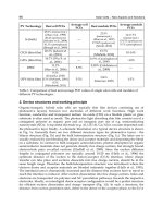
develop IMPATT devices based on Wide-Band-Gap (WBG) semiconductors (e.g. SiC and
GaN) having high critical electric field (E
C
), high carrier saturation velocity (v
S
) as well as
high thermal conductivity (K) (Table 1) [Trew et al.], since RF power output from an
7
AdvancedMicrowaveandMillimeterWave
Technologies:SemiconductorDevices,CircuitsandSystems114
IMPATT is proportional to E
C
2
v
s
2
. Moreover, high value of K is essential to ensure good
thermal stability for high-power operation of the devices. All these intrinsic material
parameters of WBG semiconductors are favorable for realizing smaller transit time, an
essential criterion for developing THz devices. The expected excellent performances of WBG
devices can also be expressed by figures of merit (FOM).
Table 1. Material properties of Si, GaAs, InP and important Wide Bandgap semiconductors.
The Baliga FOM is important for evaluation of high frequency application and Johnson’s
FOM considers the high-frequency and high-power capability of devices. Taking Baliga and
Johnson’s FOM for Si as unity, the Baliga and Johnson’s FOM for GaAs are 11.0 and 7.1,
respectively, while those for WBG semiconductor SiC are 29.0 and 278 and those for GaN
are 77.8 and 756. Hence, SiC and GaN are found to be superior to both conventional Si and
GaAs for high-frequency and high-power operation. Thus, in a bid to find single small-sized
MM-wave and THz power sources, it is interesting to study the prospects of WBG
semiconductor based IMPATT diodes.
Semiconductor
Si
GaAs
6H-SiC
4H-SiC
3C-
SiC
WZ-
GaN
ZB-
GaN
InP
Diamond
Bandgap
(E
g
) (eV)
1.12 1.43 3.03 3.26 2.2 3.45 3.28 1.35 5.45
Critical
Electric
Breakdown
field (E
C
)
(10
7
V.m
-1
)
3.0 4.0 25.0
(║ to
c-axis)
22.0
(║ to
c-axis)
21.2 20.0 20.0 5.0 100.0
Relative
dielectric
constant (€
r
)
11.9 13.1 9.66 9.7 9.7 8.9 9.7 12.5 5.5
Electron mobility
(µ
n
)
(m
2
V
-1
s
-1
)
0.15 0.85 0.04
(║ to c-axis)
0.05
(┴ to c- axis)
0.10
(both ║
and ┴ to
c- axis)
0.075
0.125 0.100 0.54 0.22
Hole mobility
(µ
p
)
(m
2
V
-1
s
-1
)
0.06 0.04 0.01 0.01 0.004 0.085 0.035 0.02 0.085
Saturated carrier
drift velocity (v
s
)
(║ to c-axis)
(10
5
ms
-1
)
1.0 1.2 2.0 2.0 2.2 2.5 2.0 2.2 2.7
Thermal
Conductivity (K)
(Wm
-1
K
-1
)
150.0 46.0 490.0 490.0 320.0 225.0 130.0 69.0 2200.0
In this Chapter, the DC and high-frequency characteristics of SiC and GaN based IMPATT
devices at MM-wave and THz region will be presented first. This will be followed by the
photo-sensitivity and experimental feasibility studies of the new-class of IMPATT devices.
2. IMPATT diode: brief history of development.
IMPATT is an acronym of IMPact ionization Avalanche Transit Time, which reflects the
mechanism of its operation. In its simplest form, an IMPATT is a p-n junction diode
reversed biased to breakdown, in which an avalanche of electron-hole pair is produced in
the high-field region of the device depletion layer by ‘impact ionization’. The transit of the
carriers through the depletion layer leads to generation of microwave and MM-waves when
the device is tuned in a suitable microwave and MM-wave cavity. These diodes exhibit
negative resistance at microwave and MM-wave frequencies due to two electronic delays,
viz., (i) ‘avalanche build-up delay’ due to ‘impact ionization’ leading to avalanche
multiplication of charge carriers and (ii) ‘transit time delay’ due to the saturation of drift
velocity of charge carriers moving under the influence of a high electric field.
The working principles of the device were first described by Read in 1958. However, the idea
of obtaining a negative resistance from a reversed biased p-n junction dates back to an
earlier paper (1954) by Shockley, in which he showed that when an electron bunch from a
forward biased cathode is injected into the depletion layer of a reversed biased p-n junction
a ‘transit time negative resistance’ is produced as the electrons drift across the high field
region. The negative resistance from such early devices was found to be small and
microwave power output was low. Read showed that an improved negative resistance is
obtained when impact ionization is used to inject the electrons. He showed that the
properties of charge carriers in a semiconductor i.e. (i) avalanche multiplication by impact
ionization and (ii) transit time delay of charge carriers due to saturation of drift velocity at
high electric fields, could be suitably combined in a reverse-biased p-n junction to produce a
microwave negative resistance. By exploiting the time delay required to build up an
avalanche discharge by impact ionization, coupled with Shockley’s transit time delay, he
showed that efficient microwave oscillation could be realized in his proposed p
+
n i n
+
diode. However, due to the complicated nature of the Read structure, it was not until 1965
that the first experimental Read diode was fabricated. In the early 1965 Johnston et al., from
Bell Laboratories, first made a successful experimental observation of microwave
oscillations from a simple Si p-n junction diode. This study showed that the complicated
Read structure was not essential required for generating microwave oscillations. On the
basis of a small-signal analysis, T. Misawa showed that negative resistance would occur in a
reverse biased p-n junction of any arbitrary doping profile. Since then, rapid advances have
been made towards further development of various IMPATT structures, fabrication
techniques as well as optimum circuit design for IMPATT oscillators and amplifiers. The
frequency range of IMPATT devices can be pushed easily to MM and sub-MM wave ranges
at which comparable amount of RF power generation is hardly possible by other two-
terminal solid-state devices.
WideBandGapSemiconductorBasedHighpowerATTDiodesInTheMM-waveand
THzRegime:DeviceReliability,ExperimentalFeasibilityandPhoto-sensitivity 115
IMPATT is proportional to E
C
2
v
s
2
. Moreover, high value of K is essential to ensure good
thermal stability for high-power operation of the devices. All these intrinsic material
parameters of WBG semiconductors are favorable for realizing smaller transit time, an
essential criterion for developing THz devices. The expected excellent performances of WBG
devices can also be expressed by figures of merit (FOM).
Table 1. Material properties of Si, GaAs, InP and important Wide Bandgap semiconductors.
The Baliga FOM is important for evaluation of high frequency application and Johnson’s
FOM considers the high-frequency and high-power capability of devices. Taking Baliga and
Johnson’s FOM for Si as unity, the Baliga and Johnson’s FOM for GaAs are 11.0 and 7.1,
respectively, while those for WBG semiconductor SiC are 29.0 and 278 and those for GaN
are 77.8 and 756. Hence, SiC and GaN are found to be superior to both conventional Si and
GaAs for high-frequency and high-power operation. Thus, in a bid to find single small-sized
MM-wave and THz power sources, it is interesting to study the prospects of WBG
semiconductor based IMPATT diodes.
Semiconductor
Si
GaAs
6H-SiC
4H-SiC
3C-
SiC
WZ-
GaN
ZB-
GaN
InP
Diamond
Bandgap
(E
g
) (eV)
1.12 1.43 3.03 3.26 2.2 3.45 3.28 1.35 5.45
Critical
Electric
Breakdown
field (E
C
)
(10
7
V.m
-1
)
3.0 4.0 25.0
(║ to
c-axis)
22.0
(║ to
c-axis)
21.2 20.0 20.0 5.0 100.0
Relative
dielectric
constant (€
r
)
11.9 13.1 9.66 9.7 9.7 8.9 9.7 12.5 5.5
Electron mobility
(µ
n
)
(m
2
V
-1
s
-1
)
0.15 0.85 0.04
(║ to c-axis)
0.05
(┴ to c- axis)
0.10
(both ║
and ┴ to
c- axis)
0.075
0.125 0.100 0.54 0.22
Hole mobility
(µ
p
)
(m
2
V
-1
s
-1
)
0.06 0.04 0.01 0.01 0.004 0.085 0.035 0.02 0.085
Saturated carrier
drift velocity (v
s
)
(║ to c-axis)
(10
5
ms
-1
)
1.0 1.2 2.0 2.0 2.2 2.5 2.0 2.2 2.7
Thermal
Conductivity (K)
(Wm
-1
K
-1
)
150.0 46.0 490.0 490.0 320.0 225.0 130.0 69.0 2200.0
In this Chapter, the DC and high-frequency characteristics of SiC and GaN based IMPATT
devices at MM-wave and THz region will be presented first. This will be followed by the
photo-sensitivity and experimental feasibility studies of the new-class of IMPATT devices.
2. IMPATT diode: brief history of development.
IMPATT is an acronym of IMPact ionization Avalanche Transit Time, which reflects the
mechanism of its operation. In its simplest form, an IMPATT is a p-n junction diode
reversed biased to breakdown, in which an avalanche of electron-hole pair is produced in
the high-field region of the device depletion layer by ‘impact ionization’. The transit of the
carriers through the depletion layer leads to generation of microwave and MM-waves when
the device is tuned in a suitable microwave and MM-wave cavity. These diodes exhibit
negative resistance at microwave and MM-wave frequencies due to two electronic delays,
viz., (i) ‘avalanche build-up delay’ due to ‘impact ionization’ leading to avalanche
multiplication of charge carriers and (ii) ‘transit time delay’ due to the saturation of drift
velocity of charge carriers moving under the influence of a high electric field.
The working principles of the device were first described by Read in 1958. However, the idea
of obtaining a negative resistance from a reversed biased p-n junction dates back to an
earlier paper (1954) by Shockley, in which he showed that when an electron bunch from a
forward biased cathode is injected into the depletion layer of a reversed biased p-n junction
a ‘transit time negative resistance’ is produced as the electrons drift across the high field
region. The negative resistance from such early devices was found to be small and
microwave power output was low. Read showed that an improved negative resistance is
obtained when impact ionization is used to inject the electrons. He showed that the
properties of charge carriers in a semiconductor i.e. (i) avalanche multiplication by impact
ionization and (ii) transit time delay of charge carriers due to saturation of drift velocity at
high electric fields, could be suitably combined in a reverse-biased p-n junction to produce a
microwave negative resistance. By exploiting the time delay required to build up an
avalanche discharge by impact ionization, coupled with Shockley’s transit time delay, he
showed that efficient microwave oscillation could be realized in his proposed p
+
n i n
+
diode. However, due to the complicated nature of the Read structure, it was not until 1965
that the first experimental Read diode was fabricated. In the early 1965 Johnston et al., from
Bell Laboratories, first made a successful experimental observation of microwave
oscillations from a simple Si p-n junction diode. This study showed that the complicated
Read structure was not essential required for generating microwave oscillations. On the
basis of a small-signal analysis, T. Misawa showed that negative resistance would occur in a
reverse biased p-n junction of any arbitrary doping profile. Since then, rapid advances have
been made towards further development of various IMPATT structures, fabrication
techniques as well as optimum circuit design for IMPATT oscillators and amplifiers. The
frequency range of IMPATT devices can be pushed easily to MM and sub-MM wave ranges
at which comparable amount of RF power generation is hardly possible by other two-
terminal solid-state devices.
AdvancedMicrowaveandMillimeterWave
Technologies:SemiconductorDevices,CircuitsandSystems116
3. IMPATT structures and doping profiles
The typical doping profile of a Read diode makes its realization very difficult in practice.
There are several other structures with simpler doping profiles which also exhibits
microwave negative resistance due to IMPATT action. In practically realizable structures,
the avalanche region is not very thin as was in case of Read diode and also there is no
distinct demarcation between avalanche and drift regions. Single Drift Region (SDR) and
Double Drift Region (DDR) IMPATTs are now commonly used belong to this category.
Single drift IMPATT (SDR) structure is based on a one-sided abrupt p-n junction of the form
p
+
n n
+
or n
+
p p
+
. These diodes have a single avalanche zone of finite width located at one
end of the depletion layer near the junction followed by a single drift region. The doping
profile at the junction and at the interface of substrate and epitaxy are approximated by use
of appropriate exponential and error function. The schematic doping profile of a typical SDR
diode is shown in Figure 1. Conventional SDR diodes are fabricated with Si and GaAs as
base semiconductor material. SDR p
+
n n
+
IMPATT structure is better than n
+
p p
+
structure
because technology of n
+
substrate is more advanced and better understood than p
+
substrate. Further, the extent of the un-depleted region between the edge of the depletion
region and interface of epitaxy and substrate (un-swept epitaxy), which contributes positive
series resistance and thereby dissipates microwave power, is smaller in p
+
n n
+
structure
than complimentary n
+
p p
+
structure, since, compared to hole mobility, mobility of
electrons in most of the semiconductors are much larger owing to its lower effective mass.
The fabrication of GaAs and InP SDR IMPATTs has been mostly reported with p
+
n n
+
structure because of the advantages of better avalanche characteristics, lower loss due to un-
swept epitaxy and advanced n+ substrate technology.
Double Drift IMPATT diode is another type of structure. A DDR diode is basically a p
+
p n
n
+
(or its complementary) multilayer structure usually with a symmetrical step junction. A
typical flat profile DDR along with its schematic doping profile and E(x) profile are shown
in Figure 2. The E(x) profile is characterized by a centrally located high field (> 10
7
Vm
-1
)
around the metallurgical junction along with two low field drift regions, for electrons and
holes, on either side. The holes generated in the avalanche region drift through the drift
region on the p-side while the generated electrons drift through the drift region on the n-
side. In comparison to the SDR structure, in case of the DDR structure contribution to
microwave power comes from the two drift regions. The second drift region in the DDR
diode, improves the efficiency, RF power density and impedance per unit area. The
impedance of an IMPATT diode can be approximated by a simple equivalent circuit which
consists of a series combination of negative resistance (R
D
) and reactance (X
D
). In the
oscillating frequency range, the magnitude of R
D
< X
D
, and thus the device reactance is
approximately that of the capacitance formed by the depletion layer of the device. In the
DDR structure, the added drift region increases the depletion layer width resulting in a
smaller capacitance and hence a large reactance per unit area. Thus, the impedance level of a
DDR diode is high as compared to that of the SDR diode. Several workers have previously
suggested that the efficiency and RF power output of SDR or DDR diodes can be enhanced
by modifying the epi-layer doping profile. The introduction of an impurity bump i.e. the
region of high doping density, considerably improves the device efficiency. Impurity bumps
can be suitably introduced in the depletion region by Molecular Beam Epitaxy (MBE) or by
ion implantation to produce high-efficieny IMPATT diodes.
Fig. 1. Schematic diode structure, electric field and droping profiles of n
++
pp
++
and p
++
n
+
SDR diodes
Fig. 2. The schematic diode structure, doping profile and field profile of a Double Drift flat
profile diode
WideBandGapSemiconductorBasedHighpowerATTDiodesInTheMM-waveand
THzRegime:DeviceReliability,ExperimentalFeasibilityandPhoto-sensitivity 117
3. IMPATT structures and doping profiles
The typical doping profile of a Read diode makes its realization very difficult in practice.
There are several other structures with simpler doping profiles which also exhibits
microwave negative resistance due to IMPATT action. In practically realizable structures,
the avalanche region is not very thin as was in case of Read diode and also there is no
distinct demarcation between avalanche and drift regions. Single Drift Region (SDR) and
Double Drift Region (DDR) IMPATTs are now commonly used belong to this category.
Single drift IMPATT (SDR) structure is based on a one-sided abrupt p-n junction of the form
p
+
n n
+
or n
+
p p
+
. These diodes have a single avalanche zone of finite width located at one
end of the depletion layer near the junction followed by a single drift region. The doping
profile at the junction and at the interface of substrate and epitaxy are approximated by use
of appropriate exponential and error function. The schematic doping profile of a typical SDR
diode is shown in Figure 1. Conventional SDR diodes are fabricated with Si and GaAs as
base semiconductor material. SDR p
+
n n
+
IMPATT structure is better than n
+
p p
+
structure
because technology of n
+
substrate is more advanced and better understood than p
+
substrate. Further, the extent of the un-depleted region between the edge of the depletion
region and interface of epitaxy and substrate (un-swept epitaxy), which contributes positive
series resistance and thereby dissipates microwave power, is smaller in p
+
n n
+
structure
than complimentary n
+
p p
+
structure, since, compared to hole mobility, mobility of
electrons in most of the semiconductors are much larger owing to its lower effective mass.
The fabrication of GaAs and InP SDR IMPATTs has been mostly reported with p
+
n n
+
structure because of the advantages of better avalanche characteristics, lower loss due to un-
swept epitaxy and advanced n+ substrate technology.
Double Drift IMPATT diode is another type of structure. A DDR diode is basically a p
+
p n
n
+
(or its complementary) multilayer structure usually with a symmetrical step junction. A
typical flat profile DDR along with its schematic doping profile and E(x) profile are shown
in Figure 2. The E(x) profile is characterized by a centrally located high field (> 10
7
Vm
-1
)
around the metallurgical junction along with two low field drift regions, for electrons and
holes, on either side. The holes generated in the avalanche region drift through the drift
region on the p-side while the generated electrons drift through the drift region on the n-
side. In comparison to the SDR structure, in case of the DDR structure contribution to
microwave power comes from the two drift regions. The second drift region in the DDR
diode, improves the efficiency, RF power density and impedance per unit area. The
impedance of an IMPATT diode can be approximated by a simple equivalent circuit which
consists of a series combination of negative resistance (R
D
) and reactance (X
D
). In the
oscillating frequency range, the magnitude of R
D
< X
D
, and thus the device reactance is
approximately that of the capacitance formed by the depletion layer of the device. In the
DDR structure, the added drift region increases the depletion layer width resulting in a
smaller capacitance and hence a large reactance per unit area. Thus, the impedance level of a
DDR diode is high as compared to that of the SDR diode. Several workers have previously
suggested that the efficiency and RF power output of SDR or DDR diodes can be enhanced
by modifying the epi-layer doping profile. The introduction of an impurity bump i.e. the
region of high doping density, considerably improves the device efficiency. Impurity bumps
can be suitably introduced in the depletion region by Molecular Beam Epitaxy (MBE) or by
ion implantation to produce high-efficieny IMPATT diodes.
Fig. 1. Schematic diode structure, electric field and droping profiles of n
++
pp
++
and p
++
n
+
SDR diodes
Fig. 2. The schematic diode structure, doping profile and field profile of a Double Drift flat
profile diode
AdvancedMicrowaveandMillimeterWave
Technologies:SemiconductorDevices,CircuitsandSystems118
Two types of such modified structures are generally possible, (i) lo-hi-lo, characterized by
three step doping profiles and (ii) hi-lo, characterized by two step doping profiles. Owing to
some of their similarities with Read structures, such as narrow localized avalanche zone,
these diodes are also called ‘Quasi Read’ diodes. Figures 3 (a-b) show the typical doping
profile, E(x) profiles of hi-lo, lo-hi-lo SDR and DDR diodes.
Fig. 3. (a) (i) Schematic diagram of Single Drift ‚high-low‘ structure, doping profile and field
profile
(ii) Schematic diagram of Single Drift ‚low-high-low‘ structure, doping profile and
field profile
Fig. 3. (b): The schematic diode structure, doping profile and typical field profile of (i) High-
Low DDR and (ii) Low-High-Low DDR IMPATT diodes
4. Basic operation principle of IMPATT diodes.
Microwave generation in an IMPATT diode can be explained on the basis of a simple Single
Drift Region (SDR) structure (Read or p
+
n n
+
or p
+
p n
+
). If a sinusoidal electric field is
applied to the device biased to the threshold of dc breakdown, an avalanche of e-h pair is
created in the avalanche region. The number of e-h pair reaches its peak after the peak of the
ac field has passed. This is because the number of e-h pairs created is proportional to the
product of ionization rate of an individual carrier, which is highest at the instant of the peak
field, and the number density of charge carrier presents at that time. Since the number
density goes on increasing as long as the applied field is added to the dc field, the peak of e-
h pair generation is delayed with respect to the ac field by a phase angle of approximately
900. This delay is known as avalanche build up delay. The current pulse of carriers thus
formed are injected into the drift zone, where the magnitude of the electric field is such (10
6
– 10
7
V m
-1
) that the carriers are able to drift with saturated velocity but unable to produce
additional carriers through impact ionization. This charge pulse crosses the ionization-free
drift zone with saturated velocity and produces a constant induced current in the external
circuit during the time of transit, W/v
S
.
The external current is approximately a rectangular wave and it develops between the phase
of π to 2π (Figure 4). The width of the drift region is so adjusted that the transit time of
carriers is half the period of the ac cycle. Thus the total phase lag between applied RF
voltage and external RF current is 1800, which gives rise to negative resistance. One may get
the first hand idea of frequency of oscillation from the approximate equation:
f
0
= v
s
/2W .
Fig. 4. Waveform of RF voltage, avalanche current and induced external current in a
IMPATT diode
5. Simulation scheme for DC and high-frequency analysis of un-illuminated
and iluminated IMPATT diodes of any doping profile
Numerical simulations have immense importance in producing guidelines for device design
and materials research. Moreover, computer studies are essential for understanding the
WideBandGapSemiconductorBasedHighpowerATTDiodesInTheMM-waveand
THzRegime:DeviceReliability,ExperimentalFeasibilityandPhoto-sensitivity 119
Two types of such modified structures are generally possible, (i) lo-hi-lo, characterized by
three step doping profiles and (ii) hi-lo, characterized by two step doping profiles. Owing to
some of their similarities with Read structures, such as narrow localized avalanche zone,
these diodes are also called ‘Quasi Read’ diodes. Figures 3 (a-b) show the typical doping
profile, E(x) profiles of hi-lo, lo-hi-lo SDR and DDR diodes.
Fig. 3. (a) (i) Schematic diagram of Single Drift ‚high-low‘ structure, doping profile and field
profile
(ii) Schematic diagram of Single Drift ‚low-high-low‘ structure, doping profile and
field profile
Fig. 3. (b): The schematic diode structure, doping profile and typical field profile of (i) High-
Low DDR and (ii) Low-High-Low DDR IMPATT diodes
4. Basic operation principle of IMPATT diodes.
Microwave generation in an IMPATT diode can be explained on the basis of a simple Single
Drift Region (SDR) structure (Read or p
+
n n
+
or p
+
p n
+
). If a sinusoidal electric field is
applied to the device biased to the threshold of dc breakdown, an avalanche of e-h pair is
created in the avalanche region. The number of e-h pair reaches its peak after the peak of the
ac field has passed. This is because the number of e-h pairs created is proportional to the
product of ionization rate of an individual carrier, which is highest at the instant of the peak
field, and the number density of charge carrier presents at that time. Since the number
density goes on increasing as long as the applied field is added to the dc field, the peak of e-
h pair generation is delayed with respect to the ac field by a phase angle of approximately
900. This delay is known as avalanche build up delay. The current pulse of carriers thus
formed are injected into the drift zone, where the magnitude of the electric field is such (10
6
– 10
7
V m
-1
) that the carriers are able to drift with saturated velocity but unable to produce
additional carriers through impact ionization. This charge pulse crosses the ionization-free
drift zone with saturated velocity and produces a constant induced current in the external
circuit during the time of transit, W/v
S
.
The external current is approximately a rectangular wave and it develops between the phase
of π to 2π (Figure 4). The width of the drift region is so adjusted that the transit time of
carriers is half the period of the ac cycle. Thus the total phase lag between applied RF
voltage and external RF current is 1800, which gives rise to negative resistance. One may get
the first hand idea of frequency of oscillation from the approximate equation:
f
0
= v
s
/2W .
Fig. 4. Waveform of RF voltage, avalanche current and induced external current in a
IMPATT diode
5. Simulation scheme for DC and high-frequency analysis of un-illuminated
and iluminated IMPATT diodes of any doping profile
Numerical simulations have immense importance in producing guidelines for device design
and materials research. Moreover, computer studies are essential for understanding the
AdvancedMicrowaveandMillimeterWave
Technologies:SemiconductorDevices,CircuitsandSystems120
properties of devices, as analytical methods do not provide accurate information regarding
the dc and high frequency parameters of these devices. In the present thesis, a generalized,
simple and more accurate dc computer simulation method that involves simultaneous
computer solution of the nonlinear Poisson’s and carrier continuity equations, as proposed
by Roy et al. [15], has been adopted. DC modeling of the IMPATT devices has been made
realistic by considering the effects of mobile space charge, inequality of ionization rates and
drift velocities of charge carriers of the base materials and also their electric field and
temperature dependence. The optimum depletion layer widths for a particular design
frequency (f
o
) are chosen from the simple transit time formula W = 0.37 v
sn,sp
/ f
o
[16]. Here
v
sn
and v
sp
are the saturated drift velocities of electrons and holes respectively.
DC field and carrier current profiles for various IMPATT structures can be obtained by
starting the computation from the field maximum position, at the metallurgical junction.
The simulation method consists of two parts: (i) DC analysis and (ii) small-signal analysis. In
the dc method, Poisson and carrier continuity equations are simultaneously solved at each
point in the depletion layer, subject to appropriate boundary conditions, as described
elsewhere [Roy et al (1985), Mukherjee et al (2007a)]. A very small space step is considered for
the accurate numerical simulation of the equations.
The DC to RF conversion efficiency () [Namordi et al. (1980)] is calculated from the semi-
quantitative formula,
(%) = (V
D
x 100) /( x V
B
) (1)
where, V
D
= voltage drop across the drift region. Also, V
D
= V
B
-V
A
, where, V
A
= voltage
drop across the avalanche region and V
B
= Breakdown voltage.
The small-signal analysis of the IMPATT diode provides significant insight into the device
physics and intrinsic properties of the devices. The range of frequencies exhibiting negative
conductance of the diode can easily be computed by the Gummel-Blue method [Gummel
Blue (1967)]. From the dc field and current profiles, the spatially dependent ionization rates
that appear in the Gummel-Blue equations are evaluated and fed as input data for the high-
frequency analysis. The edges of the depletion layer of the diode, which are fixed by the dc
analysis, are taken as the starting and end points for the high-frequency analysis. The spatial
variation of high frequency negative resistivity and reactivity in the depletion layer of the
diode are obtained under small-signal conditions by solving two second order differential
equations in R(x, ) and X(x, ).
R(x, ω) and X(x, ω) are the real and imaginary parts of the diode impedance Z (x,), such
that Z (x,) = R(x, ω) + j X(x, ω). A generalized computer algorithm for simulation of the
negative resistivity and reactivity in the space charge region is used in the analysis and
described elsewhere [Roy et al (1985), Mukherjee et al (2007a)]. The total integrated diode
negative resistance (Z
R
) and reactance (Z
x
) at a particular frequency (ω) and current density
J
DC,
are computed from numerical integration of the R(x) and X(x) profiles over the active
space-charge layer.
The high-frequency admittance characteristics, negative resistivity profiles and device
quality factor (Q) of the optimized diodes are determined by this technique after satisfying
the appropriate boundary conditions for R and X, as described elsewhere [Roy et al (1985),
Mukherjee et al (2007a)]. The diode quality factor (Q
P
) at the peak frequency, is defined as
the ratio of the imaginary part of the admittance to the real part of the admittance (at the
peak frequency), i.e.,
-Q
p
= (B
p
/-G
p
) (2)
The maximum output power density (P
output
) from the device is obtained from the
expression [Eisele et al. (1997)]:
P
output
= (V
RF
2
. |-G
P
|)/2 (3)
The diode negative conductance at the optimum frequency |-G
P
| is normalized to the area
of the diode. V
RF
(amplitude of the RF swing) is taken as V
B
/2, assuming a 50% modulation
of the breakdown voltage, V
B
.
The value of series resistance (R
S
) is determined from the admittance characteristics using a
realistic analysis by Gummel-Blue [Gummel Blue (1967)] and Adlerstein [Adlerstein et al
(1983)]. Under small-signal approximation, the steady state condition for oscillations is
given by:
G
L
(ω) = |-G (ω)| – [B (ω)]
2
R
S
(ω) (4)
where G
L
is the load conductance. This relation provides minimum uncertainty in G
L
at low
power oscillation threshold. Therefore, R
S
can be calculated from equation (4), considering
the value of G
L
as nearly equal to the diode conductance (-G) at resonance.
The leakage current (J
s
), entering the depletion region of the reversed biased p-n junction of
an IMPATT diode, is normally due to thermally-generated electrons and holes [J
S
= J
ns (th)
+
J
ps (th)
] and it is so small that current multiplication factor
M
n, p
= J
o
/[J
ns (th)
or J
ps (th)
] [J
o
= bias current density] (5)
can be considered to be infinitely large. Thus the enhancement of the leakage current under
optical illumination of the devices is manifested by the lowering of M
n,p
. The effect of
shining light from the junction side in a TM (Top Mounted) IMPATT structure, as shown in
Figure 5(a), is to generate an electron-dominated photocurrent. The expression for electron
current multiplication factor then changes to
M
n
= J
o
/ [J
ns (th)
+ J
ns (opt)
], (6)
[J
ns (opt)
= saturation current due to photoelectrons].
Thus, the photoelectrons reduce the value of M
n
, while the value of M
p
remains unchanged.
Similarly, the effect of shining light from the substrate side (n
++
edge) in a FC (Flip Chip)
IMPATT structure (Figure 5(b)) is to generate a hole-dominated photo-current that modifies
the expression for hole current multiplication factor to
M
p
= J
o
/ [J
ps (th)
+ J
ps (opt)
] (7)
(J
ps (opt)
= saturation current due to photo-generated holes). Thus the photo-generated holes
reduce the value of M
p
while the value of M
n
remains unchanged.
In order to assess the role of leakage current in controlling the dynamic properties of
IMPATT oscillators at MM-wave and THz frequencies, simulation experiments are carried
out on the effect of M
n
(keeping M
p
very high ~ 10
6
) and M
P
(keeping M
n
very high ~ 10
6
) on
(i) the high-frequency admittance characteristics (ii) the negative resistivity profiles, (iii) the
WideBandGapSemiconductorBasedHighpowerATTDiodesInTheMM-waveand
THzRegime:DeviceReliability,ExperimentalFeasibilityandPhoto-sensitivity 121
properties of devices, as analytical methods do not provide accurate information regarding
the dc and high frequency parameters of these devices. In the present thesis, a generalized,
simple and more accurate dc computer simulation method that involves simultaneous
computer solution of the nonlinear Poisson’s and carrier continuity equations, as proposed
by Roy et al. [15], has been adopted. DC modeling of the IMPATT devices has been made
realistic by considering the effects of mobile space charge, inequality of ionization rates and
drift velocities of charge carriers of the base materials and also their electric field and
temperature dependence. The optimum depletion layer widths for a particular design
frequency (f
o
) are chosen from the simple transit time formula W = 0.37 v
sn,sp
/ f
o
[16]. Here
v
sn
and v
sp
are the saturated drift velocities of electrons and holes respectively.
DC field and carrier current profiles for various IMPATT structures can be obtained by
starting the computation from the field maximum position, at the metallurgical junction.
The simulation method consists of two parts: (i) DC analysis and (ii) small-signal analysis. In
the dc method, Poisson and carrier continuity equations are simultaneously solved at each
point in the depletion layer, subject to appropriate boundary conditions, as described
elsewhere [Roy et al (1985), Mukherjee et al (2007a)]. A very small space step is considered for
the accurate numerical simulation of the equations.
The DC to RF conversion efficiency () [Namordi et al. (1980)] is calculated from the semi-
quantitative formula,
(%) = (V
D
x 100) /( x V
B
) (1)
where, V
D
= voltage drop across the drift region. Also, V
D
= V
B
-V
A
, where, V
A
= voltage
drop across the avalanche region and V
B
= Breakdown voltage.
The small-signal analysis of the IMPATT diode provides significant insight into the device
physics and intrinsic properties of the devices. The range of frequencies exhibiting negative
conductance of the diode can easily be computed by the Gummel-Blue method [Gummel
Blue (1967)]. From the dc field and current profiles, the spatially dependent ionization rates
that appear in the Gummel-Blue equations are evaluated and fed as input data for the high-
frequency analysis. The edges of the depletion layer of the diode, which are fixed by the dc
analysis, are taken as the starting and end points for the high-frequency analysis. The spatial
variation of high frequency negative resistivity and reactivity in the depletion layer of the
diode are obtained under small-signal conditions by solving two second order differential
equations in R(x, ) and X(x, ).
R(x, ω) and X(x, ω) are the real and imaginary parts of the diode impedance Z (x,), such
that Z (x,) = R(x, ω) + j X(x, ω). A generalized computer algorithm for simulation of the
negative resistivity and reactivity in the space charge region is used in the analysis and
described elsewhere [Roy et al (1985), Mukherjee et al (2007a)]. The total integrated diode
negative resistance (Z
R
) and reactance (Z
x
) at a particular frequency (ω) and current density
J
DC,
are computed from numerical integration of the R(x) and X(x) profiles over the active
space-charge layer.
The high-frequency admittance characteristics, negative resistivity profiles and device
quality factor (Q) of the optimized diodes are determined by this technique after satisfying
the appropriate boundary conditions for R and X, as described elsewhere [Roy et al (1985),
Mukherjee et al (2007a)]. The diode quality factor (Q
P
) at the peak frequency, is defined as
the ratio of the imaginary part of the admittance to the real part of the admittance (at the
peak frequency), i.e.,
-Q
p
= (B
p
/-G
p
) (2)
The maximum output power density (P
output
) from the device is obtained from the
expression [Eisele et al. (1997)]:
P
output
= (V
RF
2
. |-G
P
|)/2 (3)
The diode negative conductance at the optimum frequency |-G
P
| is normalized to the area
of the diode. V
RF
(amplitude of the RF swing) is taken as V
B
/2, assuming a 50% modulation
of the breakdown voltage, V
B
.
The value of series resistance (R
S
) is determined from the admittance characteristics using a
realistic analysis by Gummel-Blue [Gummel Blue (1967)] and Adlerstein [Adlerstein et al
(1983)]. Under small-signal approximation, the steady state condition for oscillations is
given by:
G
L
(ω) = |-G (ω)| – [B (ω)]
2
R
S
(ω) (4)
where G
L
is the load conductance. This relation provides minimum uncertainty in G
L
at low
power oscillation threshold. Therefore, R
S
can be calculated from equation (4), considering
the value of G
L
as nearly equal to the diode conductance (-G) at resonance.
The leakage current (J
s
), entering the depletion region of the reversed biased p-n junction of
an IMPATT diode, is normally due to thermally-generated electrons and holes [J
S
= J
ns (th)
+
J
ps (th)
] and it is so small that current multiplication factor
M
n, p
= J
o
/[J
ns (th)
or J
ps (th)
] [J
o
= bias current density] (5)
can be considered to be infinitely large. Thus the enhancement of the leakage current under
optical illumination of the devices is manifested by the lowering of M
n,p
. The effect of
shining light from the junction side in a TM (Top Mounted) IMPATT structure, as shown in
Figure 5(a), is to generate an electron-dominated photocurrent. The expression for electron
current multiplication factor then changes to
M
n
= J
o
/ [J
ns (th)
+ J
ns (opt)
], (6)
[J
ns (opt)
= saturation current due to photoelectrons].
Thus, the photoelectrons reduce the value of M
n
, while the value of M
p
remains unchanged.
Similarly, the effect of shining light from the substrate side (n
++
edge) in a FC (Flip Chip)
IMPATT structure (Figure 5(b)) is to generate a hole-dominated photo-current that modifies
the expression for hole current multiplication factor to
M
p
= J
o
/ [J
ps (th)
+ J
ps (opt)
] (7)
(J
ps (opt)
= saturation current due to photo-generated holes). Thus the photo-generated holes
reduce the value of M
p
while the value of M
n
remains unchanged.
In order to assess the role of leakage current in controlling the dynamic properties of
IMPATT oscillators at MM-wave and THz frequencies, simulation experiments are carried
out on the effect of M
n
(keeping M
p
very high ~ 10
6
) and M
P
(keeping M
n
very high ~ 10
6
) on
(i) the high-frequency admittance characteristics (ii) the negative resistivity profiles, (iii) the
AdvancedMicrowaveandMillimeterWave
Technologies:SemiconductorDevices,CircuitsandSystems122
device quality factor (Q) and (iv) of SDR and DDR diodes for both flat and SLHL structures,.
The details of mathematical calculations based on modified boundary conditions due to
enhancement of leakage current are described elsewhere [Mazumder et al. (1993)].
6. Application and State-of-the-art THz-sources
The ‘terahertz gap’ that lies between the infrared and millimeter regions of the
electromagnetic spectrum has recently become experimentally available. Terahertz (THz)
waves, or T-rays, bridge the gap between electronics and photonics, have novel properties
Fig. 5. (a): Schematic diagram of Top Mounted DDR IMPATT diode under optical-
illumination
Fig. 5. (b): Schematic diagram of Flip-Chip DDR IMPATT diode under optical- illumination
and interact uniquely with many materials. The interest in THz was spawned both by
researchers utilizing the microwave end of the spectrum and wants to work with shorter
wavelengths, and researchers at the infrared end who saw the need for working with longer
wavelengths. THz science is rapidly developing in Europe, US, Australia, Japan as well as in
rest of the world. There is strong interest in the exploitation of the THz frequency range in
virtually all fields of basic natural science (physics, chemistry, biology) as well as medicine
[Trew (2005)]. Across Europe, a number of research groups at universities and in industry
are working on THz science and technologies. Indeed, in the last few years the U.S. Army
and the Department of Defence have focused on the advancements of THz-frequency
electronic technology and on novel applications of THz-frequency sensing. Since 1999,
Terahertz imaging [Wang et al. (2003)] has become a very important application, since it may
make possible a single step removal process. This will enable improved detection rates of
unhealthy tissue during surgery and should lead to a decrease in the number of repeat
surgeries and in morbidity. Material spectroscopy and Biomedical sensing [Naftaly et al.
(2005) and Watanabe et al (2004)] is perhaps the most rapidly developing of all THz
applications. THz imaging of pathogens such as anthrax is also possible and that provides
novel approaches for counter-terrorism. Terahertz imaging techniques are also used for
planetary and cometary sensing as well in the earth-based studies which include monitoring
of ozone depletion.
Spectroscopy was among the first applications of THz technology, for instance, in the
development of basic THz fingerprints of simple molecules, such as water, carbon monoxide
and ozone. Various rotational, vibrational and translational modes of complex organic
molecules, including bio-molecules are within the THz range. These modes are unique to a
particular molecule, and thus it is possible to obtain a ‘Terahertz fingerprint’ allowing for
the identification of those chemical substances. The application of T-rays opens the
possibilities for fast DNA analysis — in both areas of disease detection and forensics. Since
THz radiation is non-ionizing, it has many potential medical applications. Apart from
spectroscopic characterization, T-rays can also provide X-ray-like images. In fact, Terahertz
medical imaging presents a unique solution for a variety of health-related problem, such as
tissue identification through its water content, dental cavity detection and liver cancer
detection [Nishizawa et al. (2005)]. The most important fact is that, as the photon energy of
THz is much less compared to X-ray, it is not considered intrinsically harmful to living
tissues as are of X-ray. It has the ability to penetrate a few millimeters of the uppermost skin
layer, and thus the early detection of skin cancer is possible.
Scientists believe that the Terahertz spectrum is one of the critical technologies for defence
against suicide bombers and other terrorist activities [Karpowicz et al. (2005)]. Now-a-days,
researchers have focused their attention on the potential applications of Terahertz rays for
directly detecting and imaging concealed weapons and explosives. Terahertz radiation can
be transmitted through most non-metallic and non-polar mediums. When a Terahertz
system is used properly, people can see through concealing barriers such as packaging,
corrugated cardboard, walls, clothing, shoes, book bags, pill coatings, etc. Once the rays
penetrate those materials, they can also characterize what might be hidden –be they
explosives, chemical agents or others, based on a spectral fingerprint. Undoubtedly, security
systems of the near future will incorporate THz technologies. It will be increasingly
necessary to scan for biological, chemical and other weapons in a manner that is non-
invasive and fast. Terahertz sensing provides advantages to short-range radar sensing, as
they can penetrate through fog further than optical radiation. The wavelength being short
enough, it provides significantly higher bandwidth than microwaves. However, the
wavelength is long enough than infrared to reduce Rayleigh scattering and thus it find its
application in short-range battlefield communication, where smoke prevails the infrared
transmission. The advantage of THz over IR for indoor applications is that it occupies an
WideBandGapSemiconductorBasedHighpowerATTDiodesInTheMM-waveand
THzRegime:DeviceReliability,ExperimentalFeasibilityandPhoto-sensitivity 123
device quality factor (Q) and (iv) of SDR and DDR diodes for both flat and SLHL structures,.
The details of mathematical calculations based on modified boundary conditions due to
enhancement of leakage current are described elsewhere [Mazumder et al. (1993)].
6. Application and State-of-the-art THz-sources
The ‘terahertz gap’ that lies between the infrared and millimeter regions of the
electromagnetic spectrum has recently become experimentally available. Terahertz (THz)
waves, or T-rays, bridge the gap between electronics and photonics, have novel properties
Fig. 5. (a): Schematic diagram of Top Mounted DDR IMPATT diode under optical-
illumination
Fig. 5. (b): Schematic diagram of Flip-Chip DDR IMPATT diode under optical- illumination
and interact uniquely with many materials. The interest in THz was spawned both by
researchers utilizing the microwave end of the spectrum and wants to work with shorter
wavelengths, and researchers at the infrared end who saw the need for working with longer
wavelengths. THz science is rapidly developing in Europe, US, Australia, Japan as well as in
rest of the world. There is strong interest in the exploitation of the THz frequency range in
virtually all fields of basic natural science (physics, chemistry, biology) as well as medicine
[Trew (2005)]. Across Europe, a number of research groups at universities and in industry
are working on THz science and technologies. Indeed, in the last few years the U.S. Army
and the Department of Defence have focused on the advancements of THz-frequency
electronic technology and on novel applications of THz-frequency sensing. Since 1999,
Terahertz imaging [Wang et al. (2003)] has become a very important application, since it may
make possible a single step removal process. This will enable improved detection rates of
unhealthy tissue during surgery and should lead to a decrease in the number of repeat
surgeries and in morbidity. Material spectroscopy and Biomedical sensing [Naftaly et al.
(2005) and Watanabe et al (2004)] is perhaps the most rapidly developing of all THz
applications. THz imaging of pathogens such as anthrax is also possible and that provides
novel approaches for counter-terrorism. Terahertz imaging techniques are also used for
planetary and cometary sensing as well in the earth-based studies which include monitoring
of ozone depletion.
Spectroscopy was among the first applications of THz technology, for instance, in the
development of basic THz fingerprints of simple molecules, such as water, carbon monoxide
and ozone. Various rotational, vibrational and translational modes of complex organic
molecules, including bio-molecules are within the THz range. These modes are unique to a
particular molecule, and thus it is possible to obtain a ‘Terahertz fingerprint’ allowing for
the identification of those chemical substances. The application of T-rays opens the
possibilities for fast DNA analysis — in both areas of disease detection and forensics. Since
THz radiation is non-ionizing, it has many potential medical applications. Apart from
spectroscopic characterization, T-rays can also provide X-ray-like images. In fact, Terahertz
medical imaging presents a unique solution for a variety of health-related problem, such as
tissue identification through its water content, dental cavity detection and liver cancer
detection [Nishizawa et al. (2005)]. The most important fact is that, as the photon energy of
THz is much less compared to X-ray, it is not considered intrinsically harmful to living
tissues as are of X-ray. It has the ability to penetrate a few millimeters of the uppermost skin
layer, and thus the early detection of skin cancer is possible.
Scientists believe that the Terahertz spectrum is one of the critical technologies for defence
against suicide bombers and other terrorist activities [Karpowicz et al. (2005)]. Now-a-days,
researchers have focused their attention on the potential applications of Terahertz rays for
directly detecting and imaging concealed weapons and explosives. Terahertz radiation can
be transmitted through most non-metallic and non-polar mediums. When a Terahertz
system is used properly, people can see through concealing barriers such as packaging,
corrugated cardboard, walls, clothing, shoes, book bags, pill coatings, etc. Once the rays
penetrate those materials, they can also characterize what might be hidden –be they
explosives, chemical agents or others, based on a spectral fingerprint. Undoubtedly, security
systems of the near future will incorporate THz technologies. It will be increasingly
necessary to scan for biological, chemical and other weapons in a manner that is non-
invasive and fast. Terahertz sensing provides advantages to short-range radar sensing, as
they can penetrate through fog further than optical radiation. The wavelength being short
enough, it provides significantly higher bandwidth than microwaves. However, the
wavelength is long enough than infrared to reduce Rayleigh scattering and thus it find its
application in short-range battlefield communication, where smoke prevails the infrared
transmission. The advantage of THz over IR for indoor applications is that it occupies an
AdvancedMicrowaveandMillimeterWave
Technologies:SemiconductorDevices,CircuitsandSystems124
extremely quiet band without noise or background clutter. Conventional wireless
techniques for communication use microwaves at very low power. THz could increase the
rate of information transfer as well as the volume. Now-a-days wireless communication
technology requires more bandwidth for communication and data transfer. Although the
high atmospheric attenuation at terahertz frequencies makes it difficult to have a long range
mobile-communication, however a high-bandwidth, short-range and line of sight wireless
link is completely realizable [Nagatsuma et al. (2004)]. On the other hand, atmospheric
attenuation has an advantage in the reduction of coverage range of the signal in military
applications to avoid communication being overheard or in frequency re-use application to
avoid signal interfering.
Although all other areas of the electromagnetic spectrum are used in current technologies,
development of technologies in the THz region is very difficult. The reason for this lies in
the lack of suitable THz sources and receivers. Thus a critical roadblock to full exploitation
of the THz band is lack of reliable, powerful (0.1W – 10.0 W CW), efficient, compact and
relatively inexpensive THz radiation sources. Some of the existing THz sources are: electron
beam sources, optically pumped far-infrared gas lasers, frequency multipliers,
photoconductive emitters, terahertz semiconductor lasers, terahertz photo-mixers, solid-
state sources, etc.
Among electron beam sources, Gyrotrons [Flech et al. (1999)], free electron lasers
[Krishnagopal et al. (2004)], backward wave oscillators (BWO) [Dobroiu et al. (2004)] are
capable of generating high-power at THz frequency region. Gyrotrons with 1 MW power at
140 GHz [Dammertz et al. (2002)] is feasible. Free electron lasers (FEL) are capable of
operating virtually over the entire electromagnetic spectrum. A free electron laser at the
University of California works at far infrared region and can generate 1 KW quasi-
continuous wave signal at 300 GHz. BWOs can generate 50.0 mW of power at 300 GHz
down to a few mW at 1 THz [Schmidt et al. (2002)]. The commercially available systems
provided by Russian Company ISTOK can generate 1- 10 mW output power within the
frequency range 177 GHz – 1.1 THz. Complete systems are heavy and large and need high
bias voltage and water cooling systems [Ives et al. (2003)] , but the systems are much smaller
than FEL and Gyrotrons. Electron beam devices are bulky and needs extremely high fields
as well as high current densities which are main disadvantages of these devices.
Optically pumped far infrared gas lasers can produce terahertz signals. These THz sources
consists of CO
2
pump laser injected into a cavity filled with a gas that help to produce THz
signal [Chao et al. (2009)]. Semiconductor lasers show great promise for narrowband THz
generation. Such lasers have many inherent limitations including low efficiency, low output
power and the need for cryogenic cooling to maintain lasing conditions. The Quantum
Cascade Laser (QCL) is the most promising THz semiconductor laser. Barbieri et al. has
fabricated a continuous wave QCL that can generate 25 µW power at 4.4 THz at 52 K
[Barbieri et al.(2003)]. Recently, the highest power THz source, pumped by an eye-safe,
narrow band fiber laser system with an output of 26.4 mW, has been developed [Leigh et al.
(2009)].
Among all two terminal solid-state sources, higher RF power levels of 23 µW at the
fundamental frequency of 342 GHz and 0.6 µW at the third harmonic frequency of 1.02 THz
is measured with Resonant Tunneling Diode (RTD) in the GaInAs/AlAs material systems,
but these devices were operated in a “quasi CW mode” with a pulse length of 0.3 ms and a
repetition rate of 300 Hz [Orihashi et al. (2005)]. State-of-the-art Gunn devices generate 0.2 – 5
µW power at 400 – 560 GHz frequencies [Eisele et al. (2005)]. Presently the maximum
operating frequency range of TUNNETT devices is 355 GHz with power output of 140 µW
[Eisele (2005)]. IMPact Avalanche Transit Time (IMPATT) diodes are recognized as the most
powerful two terminal sources. Higher RF power and oscillation frequency were achieved
from these devices by cooling he heat-sink of the diode and the waveguide circuit to 77K
(liquid nitrogen) [2.11]. State-of-the-art IMPATT devices generate 2 mW- 7.5 mW power in
the 300-400 GHz frequency range [Ishibashi et al. (1977)].
The above review shows that compact, low-cost but high-power and efficient THz sources
are still lacking. Researchers have focused their attention in developing such THz sources to
overcome the present limitation of THz systems. Research is continuing to increase the
frequency and power level of conventional Si and GaAs based IMPATT devices to reach the
THz region and also using alternate semiconductor material, such as, SiC and GaN together
with improved fabrication techniques.
7. WBG semiconductors for fabricating high-power IMPATTs
The material parameters of the base semiconductors play an important role in deciding the
operating frequency and output power level of IMPATT devices. So, the base semiconductor
material should be chosen selectively to design high-power, high-frequency devices. The
classification of WBG semiconductors is varied. Since the primary physical properties of a
semiconductor scale to a certain degree with the energy gap, this parameter provides a
reasonable classification scheme. However, comparison with Si and GaAs are common,
because of the importance of these common materials. So, in general a WBG semiconductor
is classified as a material with a bandgap at least twice the bandgap of Si. This gives a range
from about 2eV (with InN and 3C-SiC) up to 6 eV (with AlN and diamond). WBG
semiconductors, especially the Silicon Carbide (SiC) family and III-Nitride (GaN and its
compounds) family are relatively attractive for developing new generation devices.
Although the properties of these materials are very favorable, they are not as technologically
mature as Si and GaAs. Rapid progress has been made in resolving the technological
problems of the wide band gap semiconductors related to crystal growth, contact formation,
material purity and quality.
SiC is recognized as a semiconductor of great importance in electronic applications because
of its distinct properties, the possibility of easy growth on a native oxide, and the presence
of numerous polytypes [Elasser et al. (2002)]. The SiC family of semiconductor contains the
same semiconductor material grown in many polytypes. The most commonly grown SiC
materials are 4H-SiC, 6H-SiC, 3C-SiC. SiC, although of varied polytypes, generally have
high carrier saturation velocity and high thermal conductivity, which make them suitable
for high-temperature (above 800K), high-frequency (Terahertz region) applications. Cree
Research Inc. was the first commercial vendor of SiC wafers which are commercially
available as 4–inch wafers of 4H-SiC. It is well known that SiC wafer quality deficiencies are
delaying the realization of outstandingly superior 4H-SiC high-power semiconductor
devices. While efforts to date have centered on eradicating micropipes, 4H-SiC wafers and
epilayers also contain elementary screw dislocations in densities of the order of thousands
per cm
2
, nearly 100 fold micropipe densities [Dudley et al. (1995)]. While not nearly as
detrimental to SiC device performances as micropipes, it was shown earlier that diodes
containing elementary screw dislocations exhibit a 5% to 35% reduction in breakdown
WideBandGapSemiconductorBasedHighpowerATTDiodesInTheMM-waveand
THzRegime:DeviceReliability,ExperimentalFeasibilityandPhoto-sensitivity 125
extremely quiet band without noise or background clutter. Conventional wireless
techniques for communication use microwaves at very low power. THz could increase the
rate of information transfer as well as the volume. Now-a-days wireless communication
technology requires more bandwidth for communication and data transfer. Although the
high atmospheric attenuation at terahertz frequencies makes it difficult to have a long range
mobile-communication, however a high-bandwidth, short-range and line of sight wireless
link is completely realizable [Nagatsuma et al. (2004)]. On the other hand, atmospheric
attenuation has an advantage in the reduction of coverage range of the signal in military
applications to avoid communication being overheard or in frequency re-use application to
avoid signal interfering.
Although all other areas of the electromagnetic spectrum are used in current technologies,
development of technologies in the THz region is very difficult. The reason for this lies in
the lack of suitable THz sources and receivers. Thus a critical roadblock to full exploitation
of the THz band is lack of reliable, powerful (0.1W – 10.0 W CW), efficient, compact and
relatively inexpensive THz radiation sources. Some of the existing THz sources are: electron
beam sources, optically pumped far-infrared gas lasers, frequency multipliers,
photoconductive emitters, terahertz semiconductor lasers, terahertz photo-mixers, solid-
state sources, etc.
Among electron beam sources, Gyrotrons [Flech et al. (1999)], free electron lasers
[Krishnagopal et al. (2004)], backward wave oscillators (BWO) [Dobroiu et al. (2004)] are
capable of generating high-power at THz frequency region. Gyrotrons with 1 MW power at
140 GHz [Dammertz et al. (2002)] is feasible. Free electron lasers (FEL) are capable of
operating virtually over the entire electromagnetic spectrum. A free electron laser at the
University of California works at far infrared region and can generate 1 KW quasi-
continuous wave signal at 300 GHz. BWOs can generate 50.0 mW of power at 300 GHz
down to a few mW at 1 THz [Schmidt et al. (2002)]. The commercially available systems
provided by Russian Company ISTOK can generate 1- 10 mW output power within the
frequency range 177 GHz – 1.1 THz. Complete systems are heavy and large and need high
bias voltage and water cooling systems [Ives et al. (2003)] , but the systems are much smaller
than FEL and Gyrotrons. Electron beam devices are bulky and needs extremely high fields
as well as high current densities which are main disadvantages of these devices.
Optically pumped far infrared gas lasers can produce terahertz signals. These THz sources
consists of CO
2
pump laser injected into a cavity filled with a gas that help to produce THz
signal [Chao et al. (2009)]. Semiconductor lasers show great promise for narrowband THz
generation. Such lasers have many inherent limitations including low efficiency, low output
power and the need for cryogenic cooling to maintain lasing conditions. The Quantum
Cascade Laser (QCL) is the most promising THz semiconductor laser. Barbieri et al. has
fabricated a continuous wave QCL that can generate 25 µW power at 4.4 THz at 52 K
[Barbieri et al.(2003)]. Recently, the highest power THz source, pumped by an eye-safe,
narrow band fiber laser system with an output of 26.4 mW, has been developed [Leigh et al.
(2009)].
Among all two terminal solid-state sources, higher RF power levels of 23 µW at the
fundamental frequency of 342 GHz and 0.6 µW at the third harmonic frequency of 1.02 THz
is measured with Resonant Tunneling Diode (RTD) in the GaInAs/AlAs material systems,
but these devices were operated in a “quasi CW mode” with a pulse length of 0.3 ms and a
repetition rate of 300 Hz [Orihashi et al. (2005)]. State-of-the-art Gunn devices generate 0.2 – 5
µW power at 400 – 560 GHz frequencies [Eisele et al. (2005)]. Presently the maximum
operating frequency range of TUNNETT devices is 355 GHz with power output of 140 µW
[Eisele (2005)]. IMPact Avalanche Transit Time (IMPATT) diodes are recognized as the most
powerful two terminal sources. Higher RF power and oscillation frequency were achieved
from these devices by cooling he heat-sink of the diode and the waveguide circuit to 77K
(liquid nitrogen) [2.11]. State-of-the-art IMPATT devices generate 2 mW- 7.5 mW power in
the 300-400 GHz frequency range [Ishibashi et al. (1977)].
The above review shows that compact, low-cost but high-power and efficient THz sources
are still lacking. Researchers have focused their attention in developing such THz sources to
overcome the present limitation of THz systems. Research is continuing to increase the
frequency and power level of conventional Si and GaAs based IMPATT devices to reach the
THz region and also using alternate semiconductor material, such as, SiC and GaN together
with improved fabrication techniques.
7. WBG semiconductors for fabricating high-power IMPATTs
The material parameters of the base semiconductors play an important role in deciding the
operating frequency and output power level of IMPATT devices. So, the base semiconductor
material should be chosen selectively to design high-power, high-frequency devices. The
classification of WBG semiconductors is varied. Since the primary physical properties of a
semiconductor scale to a certain degree with the energy gap, this parameter provides a
reasonable classification scheme. However, comparison with Si and GaAs are common,
because of the importance of these common materials. So, in general a WBG semiconductor
is classified as a material with a bandgap at least twice the bandgap of Si. This gives a range
from about 2eV (with InN and 3C-SiC) up to 6 eV (with AlN and diamond). WBG
semiconductors, especially the Silicon Carbide (SiC) family and III-Nitride (GaN and its
compounds) family are relatively attractive for developing new generation devices.
Although the properties of these materials are very favorable, they are not as technologically
mature as Si and GaAs. Rapid progress has been made in resolving the technological
problems of the wide band gap semiconductors related to crystal growth, contact formation,
material purity and quality.
SiC is recognized as a semiconductor of great importance in electronic applications because
of its distinct properties, the possibility of easy growth on a native oxide, and the presence
of numerous polytypes [Elasser et al. (2002)]. The SiC family of semiconductor contains the
same semiconductor material grown in many polytypes. The most commonly grown SiC
materials are 4H-SiC, 6H-SiC, 3C-SiC. SiC, although of varied polytypes, generally have
high carrier saturation velocity and high thermal conductivity, which make them suitable
for high-temperature (above 800K), high-frequency (Terahertz region) applications. Cree
Research Inc. was the first commercial vendor of SiC wafers which are commercially
available as 4–inch wafers of 4H-SiC. It is well known that SiC wafer quality deficiencies are
delaying the realization of outstandingly superior 4H-SiC high-power semiconductor
devices. While efforts to date have centered on eradicating micropipes, 4H-SiC wafers and
epilayers also contain elementary screw dislocations in densities of the order of thousands
per cm
2
, nearly 100 fold micropipe densities [Dudley et al. (1995)]. While not nearly as
detrimental to SiC device performances as micropipes, it was shown earlier that diodes
containing elementary screw dislocations exhibit a 5% to 35% reduction in breakdown
AdvancedMicrowaveandMillimeterWave
Technologies:SemiconductorDevices,CircuitsandSystems126
voltage, higher pre-breakdown reverse leakage current, softer reverse breakdown I-V knee
and concentrated microplasmic breakdown current filaments when measured under DC
testing conditions. The cubic phase, 3C-SiC, however, is difficult to grow because of lack of a
suitable substrate, thus it receives less interest. However, in recent years, there has been
some little interest in 3C-SiC, resulting in both experimental and theoretical works. The most
difficult to grow is 2H-SiC, because of its high formation energy. The most common donors
in SiC are nitrogen (N) and phosphorous (P). N substitutes on C sites in the lattice, while P
on Si sites. The most common acceptors are aluminum (Al) and boron (B) which substitutes
on Si sites.
SiC was considered to be a promising material for fabrication of IMPATT diodes for the first
time in 1973 by Keys [Keys (1973)]. Historically, the first simulation work on modeling and
analysis of SiC IMPATT devices was done by Mehdi [Mehdi et al. (1988)]. They adopted the
drift-diffusion method for analyzing the microwave and MM-wave characteristics of these
diodes. The device operating characteristics and the power generating capabilities of the
devices were studied at four different operating frequencies, 10 GHz, 35 GHz, 60 GHz and
94 GHz. Many material parameters, such as, field and temperature dependent saturation
velocities and ionization coefficients of charge carriers in SiC were not available at that time
and hence these were not considered in the simulation scheme. Their study however
predicted that performances of SiC devices are superior to Si devices under CW mode of
operation. In 1998, Meng et al. [Meng et al. (1998)] carried out a Read-type simulation
analysis of p+n Single Drift flat profile MM-Wave IMPATT devices at 800K. The simulation
demonstrates that the efficiency (DC power density) for the device is 12.4% (6.7MW cm
-2
),
15% (4.5 MW cm
-2
) and 15.8% (3.3MW cm
-2
) for frequencies of 200, 100 and 50 GHz,
respectively. A Read diode analysis is less accurate at the efficiency fall-off frequencies
because there is no well defined avalanche region at the frequencies where efficiencies falls
off. However, the study confirms the efficiency and power advantages of MM-Wave SiC
IMPATT oscillators. Later, Zhao [Zhao et al. (2000)] have reported the Monte Carlo Particle
simulation of 4H-SiC based hi-lo SDR IMPATT diode at 200 GHz. A low voltage (Vdc = 74
V) 4H-SiC IMPATT diode was designed by them to offer an efficiency of 10% at around 200
GHz with a peak output power of 11 W.
These promising theoretical results attracted the attention of experimentalists. Several
research groups started the realization of 4H-SiC based IMPATT. In 1998, Konstantinov et
al. fabricated epitaxial p-n diodes in 4H-SiC with uniform avalanche multiplications and
breakdown [Konstantinov et al. (1998)]. They have performed photo-multiplication
measurement to determine electron and hole ionization rates. P-n junction diodes were
fabricated from p
+
-n
0
-n
+
epitaxial structures grown by vapor phase epitaxy (VPE); n0 and
n+ layers were deposited on the p+ substrates. The substrates were oriented in (0001) crystal
plane with a small off-orientation angle, 3.50 or lower. The photo-multiplication
measurement revealed that impact ionization in 4H-SiC appears to be dominated by holes, a
hole to electron ionization co-efficient ratio up to 40-50 was observed. This ionization rate
asymmetry was related to band-structure effects, to the discontinuity of the conduction
band or the electron momentum along the c-direction. The results had a qualitative
agreement with earlier studies of impact ionization in 6H-SiC. In 6H-SiC also, electron
impact ionization was strongly suppressed and that was contributed to the discontinuity of
the electron energy spectrum in the conduction band. Earlier problems in SiC device
development due to poor material quality and immature device processing techniques was
greatly overcome with the availability of production-quality substrates and the progress
made in the processing technology. Though excellent microwave performances were
demonstrated in SiC MESFETs and Static Induction transistors (SIT) [Brandt (1998)], no
experimental work was reported for SiC IMPATT devices before 2000.
First experimental success of 4H-SiC based pulsed mode IMPATT was achieved by Yuan et
al. (2001). The DC characteristics of the high-low diodes exhibited hard, sustainable
avalanche breakdown, as required for IMPATT operation. The fabricated 75 µm diameter
SiC diodes were found to oscillate at 7.75 GHz at a power level of 1 mW. However, the
output power level was significantly lower than the expected simulated value. They pointed
out that the low-power problem is related to the measurement systems, particularly the
design of the bias line. Optimization of the microwave circuit, in which the diode is
embedded, is very important to properly evaluate the device performance. Any dispute in
circuit optimization causes severe reduction in output power level. Thus, Yuan et al. made a
comment that the measured low power, as obtained by their group, does not reflect the true
power capability of SiC IMPATT. Vassilevski et al. (2001) also fabricated 4H-SiC based
IMPATT. Microwave pulsed power of 300 mW was measured at 10 GHz. Though a
comparatively higher power level was achieved, the power conversion efficiency was found
to be very low ~0.3%. To increase the output power level, Ono et al. (2005) introduced a
highly resistive guard ring that surrounds the diode periphery. The advantage of this guard
ring is to reduce the electric field at the p-n junction edge of the junction periphery. A high
current can thus be supplied through the diode without any destruction. Output power of
1.8W at 11.93 GHz was obtained from their fabricated diode and which is till date the
highest reported output power from 4H-SiC IMPATT diodes. Nevertheless this power level
is much lower than that expected. To increase the output power level, as expected from
simulation studies, the residual series resistance should be minimized. No theoretical or
experimental works on lo-hi-lo type 4H-SiC-based diodes are published by other workers.
To the best of author’s knowledge, no experimental results are available for 6H-SiC based
IMPATTs. Hence, it was established that at MM-wave region, 6H-SiC is another suitable
candidate for developing high-power IMPATT devices.
The III-Nitride family of semiconductors can fill the emerging market for
semiconductor optoelectronic devices. One of the important advantages of GaN over
SiC is the ability to form heterojunctions. The fact that GaN together with InN and
AlN, allows the formation of heterostructures provides some interesting device
possibilities. The III-Nitride family consists of the binary semiconductors; InN, AlN
and GaN, and the ternaries composed of them, Al
x
G
1-x
N and In
x
Al
1-x
N. GaN can be
grown in two phases: zinc-blende (cubic) and wurtzite (hexagonal), while the
remaining III-Nitride semiconductors only have the wurtzite polytype. The III-Nitride
family of materials has gain interest in both opto-electronic and high-power solid-state
devices. Their technological immaturity is mainly due to fabrication problems;
however in recent years, advances have been made in the wurtzite-phase versions.
Again as with the SiC family, wurtzite-phase materials receive most of the attention
because of the relative ease of growth when compared to zinc-blende GaN.
Commercial GaN based devices are grown heteroepitaxially on substrates like
Sapphire and SiC. Recently, Si has been considered as a substrate for GaN growth for
its low price, high crystalline quality and potential capabilities for integration with
traditional Si-based electronic technology. MOCVD has become the technique of choice
WideBandGapSemiconductorBasedHighpowerATTDiodesInTheMM-waveand
THzRegime:DeviceReliability,ExperimentalFeasibilityandPhoto-sensitivity 127
voltage, higher pre-breakdown reverse leakage current, softer reverse breakdown I-V knee
and concentrated microplasmic breakdown current filaments when measured under DC
testing conditions. The cubic phase, 3C-SiC, however, is difficult to grow because of lack of a
suitable substrate, thus it receives less interest. However, in recent years, there has been
some little interest in 3C-SiC, resulting in both experimental and theoretical works. The most
difficult to grow is 2H-SiC, because of its high formation energy. The most common donors
in SiC are nitrogen (N) and phosphorous (P). N substitutes on C sites in the lattice, while P
on Si sites. The most common acceptors are aluminum (Al) and boron (B) which substitutes
on Si sites.
SiC was considered to be a promising material for fabrication of IMPATT diodes for the first
time in 1973 by Keys [Keys (1973)]. Historically, the first simulation work on modeling and
analysis of SiC IMPATT devices was done by Mehdi [Mehdi et al. (1988)]. They adopted the
drift-diffusion method for analyzing the microwave and MM-wave characteristics of these
diodes. The device operating characteristics and the power generating capabilities of the
devices were studied at four different operating frequencies, 10 GHz, 35 GHz, 60 GHz and
94 GHz. Many material parameters, such as, field and temperature dependent saturation
velocities and ionization coefficients of charge carriers in SiC were not available at that time
and hence these were not considered in the simulation scheme. Their study however
predicted that performances of SiC devices are superior to Si devices under CW mode of
operation. In 1998, Meng et al. [Meng et al. (1998)] carried out a Read-type simulation
analysis of p+n Single Drift flat profile MM-Wave IMPATT devices at 800K. The simulation
demonstrates that the efficiency (DC power density) for the device is 12.4% (6.7MW cm
-2
),
15% (4.5 MW cm
-2
) and 15.8% (3.3MW cm
-2
) for frequencies of 200, 100 and 50 GHz,
respectively. A Read diode analysis is less accurate at the efficiency fall-off frequencies
because there is no well defined avalanche region at the frequencies where efficiencies falls
off. However, the study confirms the efficiency and power advantages of MM-Wave SiC
IMPATT oscillators. Later, Zhao [Zhao et al. (2000)] have reported the Monte Carlo Particle
simulation of 4H-SiC based hi-lo SDR IMPATT diode at 200 GHz. A low voltage (Vdc = 74
V) 4H-SiC IMPATT diode was designed by them to offer an efficiency of 10% at around 200
GHz with a peak output power of 11 W.
These promising theoretical results attracted the attention of experimentalists. Several
research groups started the realization of 4H-SiC based IMPATT. In 1998, Konstantinov et
al. fabricated epitaxial p-n diodes in 4H-SiC with uniform avalanche multiplications and
breakdown [Konstantinov et al. (1998)]. They have performed photo-multiplication
measurement to determine electron and hole ionization rates. P-n junction diodes were
fabricated from p
+
-n
0
-n
+
epitaxial structures grown by vapor phase epitaxy (VPE); n0 and
n+ layers were deposited on the p+ substrates. The substrates were oriented in (0001) crystal
plane with a small off-orientation angle, 3.50 or lower. The photo-multiplication
measurement revealed that impact ionization in 4H-SiC appears to be dominated by holes, a
hole to electron ionization co-efficient ratio up to 40-50 was observed. This ionization rate
asymmetry was related to band-structure effects, to the discontinuity of the conduction
band or the electron momentum along the c-direction. The results had a qualitative
agreement with earlier studies of impact ionization in 6H-SiC. In 6H-SiC also, electron
impact ionization was strongly suppressed and that was contributed to the discontinuity of
the electron energy spectrum in the conduction band. Earlier problems in SiC device
development due to poor material quality and immature device processing techniques was
greatly overcome with the availability of production-quality substrates and the progress
made in the processing technology. Though excellent microwave performances were
demonstrated in SiC MESFETs and Static Induction transistors (SIT) [Brandt (1998)], no
experimental work was reported for SiC IMPATT devices before 2000.
First experimental success of 4H-SiC based pulsed mode IMPATT was achieved by Yuan et
al. (2001). The DC characteristics of the high-low diodes exhibited hard, sustainable
avalanche breakdown, as required for IMPATT operation. The fabricated 75 µm diameter
SiC diodes were found to oscillate at 7.75 GHz at a power level of 1 mW. However, the
output power level was significantly lower than the expected simulated value. They pointed
out that the low-power problem is related to the measurement systems, particularly the
design of the bias line. Optimization of the microwave circuit, in which the diode is
embedded, is very important to properly evaluate the device performance. Any dispute in
circuit optimization causes severe reduction in output power level. Thus, Yuan et al. made a
comment that the measured low power, as obtained by their group, does not reflect the true
power capability of SiC IMPATT. Vassilevski et al. (2001) also fabricated 4H-SiC based
IMPATT. Microwave pulsed power of 300 mW was measured at 10 GHz. Though a
comparatively higher power level was achieved, the power conversion efficiency was found
to be very low ~0.3%. To increase the output power level, Ono et al. (2005) introduced a
highly resistive guard ring that surrounds the diode periphery. The advantage of this guard
ring is to reduce the electric field at the p-n junction edge of the junction periphery. A high
current can thus be supplied through the diode without any destruction. Output power of
1.8W at 11.93 GHz was obtained from their fabricated diode and which is till date the
highest reported output power from 4H-SiC IMPATT diodes. Nevertheless this power level
is much lower than that expected. To increase the output power level, as expected from
simulation studies, the residual series resistance should be minimized. No theoretical or
experimental works on lo-hi-lo type 4H-SiC-based diodes are published by other workers.
To the best of author’s knowledge, no experimental results are available for 6H-SiC based
IMPATTs. Hence, it was established that at MM-wave region, 6H-SiC is another suitable
candidate for developing high-power IMPATT devices.
The III-Nitride family of semiconductors can fill the emerging market for
semiconductor optoelectronic devices. One of the important advantages of GaN over
SiC is the ability to form heterojunctions. The fact that GaN together with InN and
AlN, allows the formation of heterostructures provides some interesting device
possibilities. The III-Nitride family consists of the binary semiconductors; InN, AlN
and GaN, and the ternaries composed of them, Al
x
G
1-x
N and In
x
Al
1-x
N. GaN can be
grown in two phases: zinc-blende (cubic) and wurtzite (hexagonal), while the
remaining III-Nitride semiconductors only have the wurtzite polytype. The III-Nitride
family of materials has gain interest in both opto-electronic and high-power solid-state
devices. Their technological immaturity is mainly due to fabrication problems;
however in recent years, advances have been made in the wurtzite-phase versions.
Again as with the SiC family, wurtzite-phase materials receive most of the attention
because of the relative ease of growth when compared to zinc-blende GaN.
Commercial GaN based devices are grown heteroepitaxially on substrates like
Sapphire and SiC. Recently, Si has been considered as a substrate for GaN growth for
its low price, high crystalline quality and potential capabilities for integration with
traditional Si-based electronic technology. MOCVD has become the technique of choice
AdvancedMicrowaveandMillimeterWave
Technologies:SemiconductorDevices,CircuitsandSystems128
for the epitaxial growth of GaN material and devices [Pearton (2000)]. In MOCVD
growth, Si and Mg are used as donor and acceptor impurities, respectively. Very
recently, halide-hydride vapor phase epitaxy (HVPE) is considered as a promising
technique for the fabrication of GaN based device structures, particularly for the
GaN/SiC heterostructure. Reliable low-resistance ohmic contacts are essential for
efficient device operation. Ohmic contact processing is still a challenging area in device
technology. P- and n- type ohmic contact resistances of SiC and GaN will be discussed
in the relevant chapters of the thesis.
Despite decades of study, only recently GaN-based materials have moved from
research laboratories to commercial markets. This change was due to a rapid
progression of improvements in epitaxial growth, demonstration of p-type
conductivity and the fabrication of commercially viable devices. The fabrication of
highly efficient blue and green LEDs and diode lasers is driving the development of
GaN-technology. The robust and versatile properties of GaN make it an excellent
candidate for high-speed and high-power electronics. Interest in GaN has exploded in
past few years, leading to an expansion of its potential applications on an almost
monthly basis [Kuzuhara et al. (2009)]. This broad spectrum of applications has led
some to predict that GaN will eventually become the third most important
semiconductor material, behind Si and GaAs. High-power handeling of GaN power
transistors have already been demonstrated by fabrication of GaN High Electron
Mobility Transistors (HEMT) and Field Effect Transistor (FET) devices [Pearton (2000)].
No experimental work, however, has been reported for GaN IMPATT diodes, despite
the fact that the diodes are easier to fabricate than transistors. Till date, only a few
simulation results on GaN based IMPATT have been reported in published journals.
Meng et al. (1999) studied the MM-Wave performances of the wurtzite phase and zinc-
blende phase GaN IMPATT devices at 800K by a Read-type modeling approach. The
simulations showed that GaN wurtzite-phase p-n single drift flat-profile IMPATT
oscillators at 300 GHz have an efficiency of 11% and an RF power density of 1.6
MW.cm
-2
. Their studies confirm the efficiency and power density advantages of GaN
IMPATT oscillators. A. K. Panda et al. (2001) designed and studied the performances of
GaN based IMPATTs in the D-band. The maximum power that may be obtained from
their designed diode was 3.775 W with an efficiency of 12.5%. Moreover, their study
predicted that the wurtzite-phase GaN based IMPATT is better than its zinc- blend
counterpart, as far as breakdown voltage, power output and efficiency are concerned.
Later, Reklaitis et al. (2005) performed a Monte Carlo simulation of Wz-GaN based
near-terahertz IMPATT diode. Their analysis predicted that the device may generate a
RF power of ~ 3W at 0.45 THz with an efficiency of 18%. The diodes were found to be
more efficient than that was designed by Panda et al. This study, on the other hand,
predicted the possibilities of GaN based IMPATT diodes as efficient near-THz power
sources. Alekseev et al. (2000) performed theoretical and experimental studies for the
development and optimization of GaN based Gunn devices in the THz frequency
region. GaN Gunn-diode oscillators at 750 GHz are expected to generate power density
of 3x10
5
W cm
-2
. Before an attempt is made to fabricate GaN based IMPATT devices at
Terahertz region, reliable modeling and better understanding of high-frequency
properties of such devices are essential. Thus the author has studied the DC and
Terahertz -frequency characteristics of the GaN based flat and lo-hi-lo types IMPATT
devices at elevated junction temperature and the results will be discussed in the
concerned chapters.
Unlike GaAs, wurtzite phase GaN have different ionization rates for electrons and
holes (α
n
≠ α
P
). So from the ionization point of view, as discussed in sub-section 2.5.3,
wurtzite GaN IMPATT is expected to be noisier than GaAs IMPATT. Panda et al.
[2.188] showed that GaN based devices generate equal noise as Si-based IMPATTs, but
higher by 6-8 dB noise values compared with GaAs based devices under the same
operating conditions. However, for increased operation temperature, the noise is
found to decrease [A. K. Panda et al. (2001)]. Reklaitis et al. [Reklaitis et al.(2005)] later
studied the current voltage characteristics and the associated current noise in GaN
double drift IMPATT diodes, by Monte Carlo simulations. For values of current
multiplication factor greater than ten they observed a giant suppression of avalanche
noise down to three orders of magnitude with respect to the standard excess noise
factor. The negative feedback between fluctuations in space-charge and in number of
generated e-h pairs is found to be responsible of such a giant suppression.
8. Superiority of WBG semiconductor based IMPATTs over Conventional
diodes
4H-SiC based SDR (p
++
n n
++
) IMPATT diodes with flat and SLHL doping profiles are
designed by Mukherjee et al. (2008 a) at around Ka-band. In order to make a comparison, Si
based SDR IMPATT diode is also designed at Ka-band. The comparison reveals that 4H-SiC
based SDR diodes are capable of generating a RF power of 870.0 x 10
9
Wm
-2
with an
efficiency of 20.0 %, far better than their Si counterpart [Mukherjee et al. (2008)]. Thereafter,
the DDR IMPATT diodes are designed and studied thoroughly by Mukherjee et al. (2009 a) at
three different window frequencies: 35 GHz (Ka-band), 140 GHz (D-band) and 220 GHz (Y-
band) and the corresponding admittance plots are shown in Figures 6 (a-c). Comparative
studies of SLHL and flat-profile diodes at MM-wave window frequencies by Mukherjee et al.
(2009) reveal that the Quasi Read SLHL diodes are superior to their flat profile counterparts
in terms of power output, efficiency and negative-resistance.
Fig. 6. (a) admittance plots of 4H-SiC DDR IMPATT at Ka band
WideBandGapSemiconductorBasedHighpowerATTDiodesInTheMM-waveand
THzRegime:DeviceReliability,ExperimentalFeasibilityandPhoto-sensitivity 129
for the epitaxial growth of GaN material and devices [Pearton (2000)]. In MOCVD
growth, Si and Mg are used as donor and acceptor impurities, respectively. Very
recently, halide-hydride vapor phase epitaxy (HVPE) is considered as a promising
technique for the fabrication of GaN based device structures, particularly for the
GaN/SiC heterostructure. Reliable low-resistance ohmic contacts are essential for
efficient device operation. Ohmic contact processing is still a challenging area in device
technology. P- and n- type ohmic contact resistances of SiC and GaN will be discussed
in the relevant chapters of the thesis.
Despite decades of study, only recently GaN-based materials have moved from
research laboratories to commercial markets. This change was due to a rapid
progression of improvements in epitaxial growth, demonstration of p-type
conductivity and the fabrication of commercially viable devices. The fabrication of
highly efficient blue and green LEDs and diode lasers is driving the development of
GaN-technology. The robust and versatile properties of GaN make it an excellent
candidate for high-speed and high-power electronics. Interest in GaN has exploded in
past few years, leading to an expansion of its potential applications on an almost
monthly basis [Kuzuhara et al. (2009)]. This broad spectrum of applications has led
some to predict that GaN will eventually become the third most important
semiconductor material, behind Si and GaAs. High-power handeling of GaN power
transistors have already been demonstrated by fabrication of GaN High Electron
Mobility Transistors (HEMT) and Field Effect Transistor (FET) devices [Pearton (2000)].
No experimental work, however, has been reported for GaN IMPATT diodes, despite
the fact that the diodes are easier to fabricate than transistors. Till date, only a few
simulation results on GaN based IMPATT have been reported in published journals.
Meng et al. (1999) studied the MM-Wave performances of the wurtzite phase and zinc-
blende phase GaN IMPATT devices at 800K by a Read-type modeling approach. The
simulations showed that GaN wurtzite-phase p-n single drift flat-profile IMPATT
oscillators at 300 GHz have an efficiency of 11% and an RF power density of 1.6
MW.cm
-2
. Their studies confirm the efficiency and power density advantages of GaN
IMPATT oscillators. A. K. Panda et al. (2001) designed and studied the performances of
GaN based IMPATTs in the D-band. The maximum power that may be obtained from
their designed diode was 3.775 W with an efficiency of 12.5%. Moreover, their study
predicted that the wurtzite-phase GaN based IMPATT is better than its zinc- blend
counterpart, as far as breakdown voltage, power output and efficiency are concerned.
Later, Reklaitis et al. (2005) performed a Monte Carlo simulation of Wz-GaN based
near-terahertz IMPATT diode. Their analysis predicted that the device may generate a
RF power of ~ 3W at 0.45 THz with an efficiency of 18%. The diodes were found to be
more efficient than that was designed by Panda et al. This study, on the other hand,
predicted the possibilities of GaN based IMPATT diodes as efficient near-THz power
sources. Alekseev et al. (2000) performed theoretical and experimental studies for the
development and optimization of GaN based Gunn devices in the THz frequency
region. GaN Gunn-diode oscillators at 750 GHz are expected to generate power density
of 3x10
5
W cm
-2
. Before an attempt is made to fabricate GaN based IMPATT devices at
Terahertz region, reliable modeling and better understanding of high-frequency
properties of such devices are essential. Thus the author has studied the DC and
Terahertz -frequency characteristics of the GaN based flat and lo-hi-lo types IMPATT
devices at elevated junction temperature and the results will be discussed in the
concerned chapters.
Unlike GaAs, wurtzite phase GaN have different ionization rates for electrons and
holes (α
n
≠ α
P
). So from the ionization point of view, as discussed in sub-section 2.5.3,
wurtzite GaN IMPATT is expected to be noisier than GaAs IMPATT. Panda et al.
[2.188] showed that GaN based devices generate equal noise as Si-based IMPATTs, but
higher by 6-8 dB noise values compared with GaAs based devices under the same
operating conditions. However, for increased operation temperature, the noise is
found to decrease [A. K. Panda et al. (2001)]. Reklaitis et al. [Reklaitis et al.(2005)] later
studied the current voltage characteristics and the associated current noise in GaN
double drift IMPATT diodes, by Monte Carlo simulations. For values of current
multiplication factor greater than ten they observed a giant suppression of avalanche
noise down to three orders of magnitude with respect to the standard excess noise
factor. The negative feedback between fluctuations in space-charge and in number of
generated e-h pairs is found to be responsible of such a giant suppression.
8. Superiority of WBG semiconductor based IMPATTs over Conventional
diodes
4H-SiC based SDR (p
++
n n
++
) IMPATT diodes with flat and SLHL doping profiles are
designed by Mukherjee et al. (2008 a) at around Ka-band. In order to make a comparison, Si
based SDR IMPATT diode is also designed at Ka-band. The comparison reveals that 4H-SiC
based SDR diodes are capable of generating a RF power of 870.0 x 10
9
Wm
-2
with an
efficiency of 20.0 %, far better than their Si counterpart [Mukherjee et al. (2008)]. Thereafter,
the DDR IMPATT diodes are designed and studied thoroughly by Mukherjee et al. (2009 a) at
three different window frequencies: 35 GHz (Ka-band), 140 GHz (D-band) and 220 GHz (Y-
band) and the corresponding admittance plots are shown in Figures 6 (a-c). Comparative
studies of SLHL and flat-profile diodes at MM-wave window frequencies by Mukherjee et al.
(2009) reveal that the Quasi Read SLHL diodes are superior to their flat profile counterparts
in terms of power output, efficiency and negative-resistance.
Fig. 6. (a) admittance plots of 4H-SiC DDR IMPATT at Ka band
AdvancedMicrowaveandMillimeterWave
Technologies:SemiconductorDevices,CircuitsandSystems130
Fig. 6. (b) admittance plots of 4H-SiC DDR IMPATT at D-band
Fig. 6. (c) admittance plots of 4H-SiC DDR IMPATT at Y-band
Mukherjee et al. (2007 b) has made a systematic study on the performance of the IMPATTs
designed at higher THz frequencies: 0.5 THz and 1.85 THz. The electric field profiles and
admittance plots are shown in Figures 7 and 8 (a-b). It is interesting to note that even at the
higher THz region (1.85 THz), 4H-SiC based diode is capable of generating a power density
of 5.0x10
11
Wm
-2
with an efficiency of 9.0%. While estimating the power density, the effects
of series resistances is considered in the analysis. The values of P
max
, with and with-out R
S
,
are also studied and shown in Figures 9 (a-b).
The performances of the SLHL DDR IMPATT at THz region are further studied by
Mukherjee et al. (2007 c). It is observed that, similar to MM-wave region, in THz region also
the overall performance of SLHL diode is far better than its flat profile counterpart. It is
further interesting to observe that the magnitude of R
S
reduces significantly (15% - 30%) in
SLHL diodes compare to that in flat profile diodes. The performances of the 4H-SiC, 6H-
SiC, and 3C-SiC based THz (0.3 THz) DDR diodes are compared by Mukherjee et al (2008 b).
The study reveals that the 4H (α)-SiC based IMPATT may yield a RF power density of 36.45
x 10
10
Wm
-2
, with an efficiency of 14%, which are far better than its hexagonal (6H-SiC) and
cubic (3C-SiC) counterparts, under similar operating conditions. The above observations
definitely establish the potential of SiC based IMPATTs at MM-wave as well in the THz
region.
Fig. 7. E(x) profiles of 4H-SiC based Terabertz IMPATT diodes
Fig. 8. (a): Admittance characteristics of 4H-SiC IMPATT at 0.5 Terahertz.
WideBandGapSemiconductorBasedHighpowerATTDiodesInTheMM-waveand
THzRegime:DeviceReliability,ExperimentalFeasibilityandPhoto-sensitivity 131
Fig. 6. (b) admittance plots of 4H-SiC DDR IMPATT at D-band
Fig. 6. (c) admittance plots of 4H-SiC DDR IMPATT at Y-band
Mukherjee et al. (2007 b) has made a systematic study on the performance of the IMPATTs
designed at higher THz frequencies: 0.5 THz and 1.85 THz. The electric field profiles and
admittance plots are shown in Figures 7 and 8 (a-b). It is interesting to note that even at the
higher THz region (1.85 THz), 4H-SiC based diode is capable of generating a power density
of 5.0x10
11
Wm
-2
with an efficiency of 9.0%. While estimating the power density, the effects
of series resistances is considered in the analysis. The values of P
max
, with and with-out R
S
,
are also studied and shown in Figures 9 (a-b).
The performances of the SLHL DDR IMPATT at THz region are further studied by
Mukherjee et al. (2007 c). It is observed that, similar to MM-wave region, in THz region also
the overall performance of SLHL diode is far better than its flat profile counterpart. It is
further interesting to observe that the magnitude of R
S
reduces significantly (15% - 30%) in
SLHL diodes compare to that in flat profile diodes. The performances of the 4H-SiC, 6H-
SiC, and 3C-SiC based THz (0.3 THz) DDR diodes are compared by Mukherjee et al (2008 b).
The study reveals that the 4H (α)-SiC based IMPATT may yield a RF power density of 36.45
x 10
10
Wm
-2
, with an efficiency of 14%, which are far better than its hexagonal (6H-SiC) and
cubic (3C-SiC) counterparts, under similar operating conditions. The above observations
definitely establish the potential of SiC based IMPATTs at MM-wave as well in the THz
region.
Fig. 7. E(x) profiles of 4H-SiC based Terabertz IMPATT diodes
Fig. 8. (a): Admittance characteristics of 4H-SiC IMPATT at 0.5 Terahertz.
AdvancedMicrowaveandMillimeterWave
Technologies:SemiconductorDevices,CircuitsandSystems132
Fig. 8. (b): Admittance characteristics of 4H-SiC IMPATT at 1.8 Terahertz
Fig. 9. (a): Effect of series reristance on output power density P
max
of 4H-SiC 0.5 THz
IMPATT diode. (a) 4H-SiC IMPATT at 300K, R
s
=0.0Ω, (b) 4H-SiC IMPATT at 300K,
R
s,total
=0.386x10
-9
Ω m
2
Fig. 9. (b): Effect of series resistance on output power density (P
max
) of SiC THz IMPATT
diodes. (a) 4H-SiC IMPATT at 300K, R
s
=0.0Ω, (b) 4H-SiC IMPATT at 300K, R
s,total
=2.2x10
-11
Ω
m
2
Fig. 10. Plots of electric field profile for (a) SLHL and (b) flat-type GaN (flat-profile) SDR
IMPATT diodes. The distance of the n-side from the metallurgical junction has been
considered as negative.
WideBandGapSemiconductorBasedHighpowerATTDiodesInTheMM-waveand
THzRegime:DeviceReliability,ExperimentalFeasibilityandPhoto-sensitivity 133
Fig. 8. (b): Admittance characteristics of 4H-SiC IMPATT at 1.8 Terahertz
Fig. 9. (a): Effect of series reristance on output power density P
max
of 4H-SiC 0.5 THz
IMPATT diode. (a) 4H-SiC IMPATT at 300K, R
s
=0.0Ω, (b) 4H-SiC IMPATT at 300K,
R
s,total
=0.386x10
-9
Ω m
2
Fig. 9. (b): Effect of series resistance on output power density (P
max
) of SiC THz IMPATT
diodes. (a) 4H-SiC IMPATT at 300K, R
s
=0.0Ω, (b) 4H-SiC IMPATT at 300K, R
s,total
=2.2x10
-11
Ω
m
2
Fig. 10. Plots of electric field profile for (a) SLHL and (b) flat-type GaN (flat-profile) SDR
IMPATT diodes. The distance of the n-side from the metallurgical junction has been
considered as negative.
AdvancedMicrowaveandMillimeterWave
Technologies:SemiconductorDevices,CircuitsandSystems134
Fig. 11. Conductance (G) – Susceptance (B) plots of GaN (a) SLHL and (b) flat type SDR THz
IMPATT diodes in Terahertz region.
Fig. 12. Effect of R
s
on the negative conductance of unilluminated GaN (flat and SLHL) SDR
IMPATT diodes.
Fig. 13. Effect of photo-illumination on FC and TM illumination configurations of SiC (3C,
4H and 6H types) based terahertz DDR IMPATT diodes at room temperature (300K).
WZ-GaN based SDR (p
++
n n
++
) IMPATT diode is designed and studied by Mukherjee et al.
at around 140.0 GHz (D-band) frequency and the performances are compared with Si
IMPATT. It is found that the GaN IMPATT may generate an output-power density of
5.6x10
10
Wm
-2
with an efficiency of 23.5% at 145.0 GHz, far better than Si IMPATT. The
prospects of SDR flat and SLHL type GaN IMPATTs at 1.45 THz are simulated and the
results are reported elsewhere [Mukherjee et al. (2007 a) ]. The studies indicate that GaN
IMPATT diodes are capable of generating high power of ~2.5 W (assuming diode area =
0.5x10
-10
m
2
) at around 1.45 THz with 17% -19.0 % efficiency. The effect of series resistance
on the THz performance of the device is also studied by Mukherjee et al (2007 a). It is
interesting to note that the presence of a charge bump in flatly doped SDR structure reduces
the value of parasitic series resistance in GaN-IMPATT by ~ 22%. The electric field profiles,
admittance charecteristics and effects of series resistance on P
max
of the GaN flat and SLHL
diodes at 1.45 THz are shown in Figures 10, 11 and 12 [Mukherjee et al (2007 a)].
9. Photo-sensitivity of WBG semiconductor based IMPATTs
The effects of photo-illumination on the 4H-SiC, 6H-SiC and 3C-SiC based Top Mounted
and Flip Chip diodes are studied by Mukherjee et al (2008 b) at THz region. It is found that
the optimum frequency and THz characteristics undergo sufficient variation with increase
of the intensity of optical radiation. It is interesting to note that in all the three types of SiC
based IMPATTs, photo-generated leakage current dominated by holes (FC illimination
configuration) is more important than that dominated by electrons (TM illumination
configuration), in modulating the high frequency properties of the devices. This observation
WideBandGapSemiconductorBasedHighpowerATTDiodesInTheMM-waveand
THzRegime:DeviceReliability,ExperimentalFeasibilityandPhoto-sensitivity 135
Fig. 11. Conductance (G) – Susceptance (B) plots of GaN (a) SLHL and (b) flat type SDR THz
IMPATT diodes in Terahertz region.
Fig. 12. Effect of R
s
on the negative conductance of unilluminated GaN (flat and SLHL) SDR
IMPATT diodes.
Fig. 13. Effect of photo-illumination on FC and TM illumination configurations of SiC (3C,
4H and 6H types) based terahertz DDR IMPATT diodes at room temperature (300K).
WZ-GaN based SDR (p
++
n n
++
) IMPATT diode is designed and studied by Mukherjee et al.
at around 140.0 GHz (D-band) frequency and the performances are compared with Si
IMPATT. It is found that the GaN IMPATT may generate an output-power density of
5.6x10
10
Wm
-2
with an efficiency of 23.5% at 145.0 GHz, far better than Si IMPATT. The
prospects of SDR flat and SLHL type GaN IMPATTs at 1.45 THz are simulated and the
results are reported elsewhere [Mukherjee et al. (2007 a) ]. The studies indicate that GaN
IMPATT diodes are capable of generating high power of ~2.5 W (assuming diode area =
0.5x10
-10
m
2
) at around 1.45 THz with 17% -19.0 % efficiency. The effect of series resistance
on the THz performance of the device is also studied by Mukherjee et al (2007 a). It is
interesting to note that the presence of a charge bump in flatly doped SDR structure reduces
the value of parasitic series resistance in GaN-IMPATT by ~ 22%. The electric field profiles,
admittance charecteristics and effects of series resistance on P
max
of the GaN flat and SLHL
diodes at 1.45 THz are shown in Figures 10, 11 and 12 [Mukherjee et al (2007 a)].
9. Photo-sensitivity of WBG semiconductor based IMPATTs
The effects of photo-illumination on the 4H-SiC, 6H-SiC and 3C-SiC based Top Mounted
and Flip Chip diodes are studied by Mukherjee et al (2008 b) at THz region. It is found that
the optimum frequency and THz characteristics undergo sufficient variation with increase
of the intensity of optical radiation. It is interesting to note that in all the three types of SiC
based IMPATTs, photo-generated leakage current dominated by holes (FC illimination
configuration) is more important than that dominated by electrons (TM illumination
configuration), in modulating the high frequency properties of the devices. This observation