Evolution of dark spots in organic light emitting devices
Bạn đang xem bản rút gọn của tài liệu. Xem và tải ngay bản đầy đủ của tài liệu tại đây (5.29 MB, 148 trang )
Evolution of Dark Spots
in
Organic Light Emitting Devices
Liew Yoon Fei
NATIONAL UNIVERSITY OF SINGAPORE
2004
Evolution of Dark Spots
in
Organic Light Emitting Devices
Liew Yoon Fei
(M.Sc., NUS)
A THESIS SUBMITTED
FOR THE DEGREE OF DOCTOR OF PHILOSOPHY
DEPARTMENT OF
ELECTRICAL AND COMPUTER ENGINEERING
NATIONAL UNIVERSITY OF SINGAPORE
2004
Acknowledgements
I gratefully acknowledge and express deep appreciation to many wonderful
people who had helped to make this project succeeded. First and foremost, I am deeply
indebted for the indulgence of my family, and particularly to my parents, for their
understanding and supporting throughout the years. I would like to express my deepest
gratefulness to my wife, Shiau Yee for her unquestioning faith and support throughout
the whole project.
I would like to express my heart-most gratitude to my supervisors Professor
Chua Soo Jin and Dr. Zhu Furong for their invaluable guidance and advices. My
appreciation also goes to Professor Xu Gu and Dr. Tok Eng Soon for their friendship,
help, encouragement and discussion during my entire candidature. What I have learned
from them is truly beneficial to the rest of my life.
I would like to thank Institute of Materials Research and Engineering (IMRE)
for offering me the opportunity to pursue my research work in IMRE. My
appreciation also goes to the staffs in IMRE, Jianqiao, Weiwei, Roshan, Siew Wei,
Bee Ling, Li Wei, Kian Soo, Xiao Tao and Yanqian for their enormous help and
support all this while.
ii
Table of Contents
Acknowledgments
ii
Table of Contents
iii
Summary
vii
Abbreviations
ix
List of Figures
xi
List of Tables
xiv
List of Publications
xv
Chapter 1: Introduction and Research Overview
1
1.1 Information Display
2
1.2 Display Devices
3
1.2.1 Cathodoluminescent Displays
3
1.2.2 Non-emissive Displays
4
1.2.3 Plasma Displays
6
1.2.4 Electroluminescent (EL) Displays
7
1.2.4.1 Inorganic Light Emitting Devices
7
1.2.4.2 Organic Light Emitting Devices (OLEDs)
8
1.3 Development of OLEDs
11
iii
1.4 Remaining Challenges for OLEDs
14
1.4.1 Achieving Full Color Displays
14
1.4.2 Improving of EL Efficiency
15
1.4.3 Extending Device Operation Lifetime
16
1.5 Research Objective
17
1.6 Thesis Outline
19
Chapter 2: Literature Review
21
2.1 Principle and Operation of OLEDs
22
2.1.1 Transportation, Recombination and Electroluminescence
23
2.1.2 Quantum Efficiency
30
2.2 Device Configuration for Efficient Operation
32
2.3 Recent Development of OLEDs
40
2.3.1 Enhancement of EL Efficiency
40
2.3.2 Extension of Device Operation Lifetime
45
2.3.2.1 Intrinsic Degradation
45
2.3.2.2 Dark Spots Formation
48
Chapter 3: Experimental
52
3.1 Sample Preparation
53
3.2 Device Characterization
54
3.2.1 Current-Voltage-Luminescence and Optical Microscopy
54
3.2.2 Atomic Force Microscopy (AFM)
55
3.2.3 X-ray Photoelectron Spectroscopy (XPS)
55
iv
Chapter 4: Evolution of Dark Spots
57
4.1 Optical Image Analysis
58
4.2 Organic Layer Thickness Effect
61
4.3 Substrate Effect
64
4.4 Multilayer Effect
67
Chapter 5: Surface and Interface Analyses
70
5.1 AFM Studies
71
5.1.1 ITO Substrate
71
5.1.2 Alq
3
Films
73
5.1.3 NPB Films
76
5.1.4 Bilayer Structure
79
5.2 Spectroscopic Studies
81
5.2.1 XPS - Alq
3
Thickness
81
5.2.2 XPS - NPB Thickness
89
5.2.3 XPS Depth Profile
91
Chapter 6: Model of Dark Spot Formation
97
6.1 Galvanic Cell Formation in OLEDs
98
6.2 Model of Dark Spot Formation in OLEDs under Non-Operating
Condition
102
6.2.1 Case I: glass/NPB/Ca/Ag Device
105
6.2.2 Case II: ITO/NPB/Ca/Ag Device
106
v
Chapter 7: Anode Modification
109
7.1 Enhancement of EL Efficiency
110
7.2 Extension of Device Lifetime
114
7.2.1 Retardation of Dark Spot Growth
115
7.2.2 Intrinsic Stability
117
Chapter 8: Conclusion
119
References
125
vi
Summary
The demand for cost effective information displays has driven an increase in
effort of research into improving the performance of organic light-emitting devices
(OLEDs). Despite these attempts, the gradual decrease in electroluminescence
efficiency and increase in operating voltage remain the major hurdles that limit the
long-term stability of the OLEDs. Apart from the intrinsic instability of the organic
materials, the growth of non-emissive areas known as dark spots in OLEDs is another
limiting factor that deteriorates the device performance.
Various mechanisms have
been proposed to address the ambient-induced growth of dark spots. Recent studies
show that organic/cathode interface is mainly responsible for the formation of dark
spots. These interfacial deteriorations in OLEDs are often considered a result of
cathode delamination or insulating layer formation at the organic/cathode interface.
It is known that the dark spots in OLEDs grow when they are not operated or
are stored in ambient conditions. Many studies on the growth of dark spots have
focused mainly on devices under various operating modes. However, the initiation and
the growth mechanisms of the dark spots in OLEDs formed before the operation of the
devices are not well investigated and fully understood. In order to pursue the study of
the origin and growth behavior of these dark spots in OLEDs without external
stimulus, it is thus essential to eliminate electrical influences via non-operation mode.
In this study, an optical image analysis technique is developed to study the
growth of dark spots in OLEDs under non-operation condition. Under reflected light of
a microscope, a direct relationship between dark spots, found in the emitting area of
vii
the OLEDs, and circular features, seen in the same locations of non-operated devices,
is identified. By using this technique, the electrical field effect on dark spot formation
is eliminated. Investigation of organic/cathode and anode/organic interfaces with
respect to their morphologies and chemical states was carried out in order to reveal the
mechanism of dark spots formation in OLEDs. Atomic force microscopy (AFM) was
employed to study the morphology of ITO and organic films deposited on ITO. X-ray
photoelectron spectroscopy (XPS) was used to obtain the materials chemical states.
Results reveal that thickness and roughness of organic films do not seem to
have significant impact on the growth of dark spots. It is found that the growth of dark
spots is dependent on the anode/organic contact. Results confirm that the degradation
site for the formation of dark spots indeed occurred at the organic/cathode interface,
but has great influence from the anode/organic interface. There is no evidence of
indium and oxygen diffusion from either the cathode or the anode to the organic layer.
Therefore, indium diffusion can not be the cause of dark spot formation in OLEDs
under non-operating condition.
Based on the experimental results obtained from this study, a model of dark
spots formation in OLEDs under non-operating condition is proposed. The growth of
dark spots is associated to the corrosion or oxidation process of reactive cathode. The
growth of dark spots is accelerated by the formation of a galvanic cell between cathode
and anode in OLEDs. The galvanic cell is formed due to the presence of an internal
built-in potential, induced by a pair of dissimilar electrodes in OLEDs.
viii
Abbreviations
ac alternative current
AFM Atomic force microscopy
Alq
3
Tris-(8-hydroxyquinoline) aluminum
BE Binding Energy
CuPc Copper phthalocyanine
CRT Cathode ray tube
dc direct current
EL Electroluminescent
ETL Electron transporting layer
HOMO Highest occupied molecular orbital
HBL Hole blocking layer
HTL Hole transporting layer
ITO Indium tin oxide
J-V-L Current density-voltage-luminance
LCD Liquid crystal display
LED Light-emitting device
LUMO Lowest unoccupied molecular orbital
NPB N, N'-di(naphthalene-1-yl)-N, N'-diphenylbenzidine
OLED Organic light-emitting device
PDA Personal digital assistant
PDP Plasma panel display
PLED Polymer light-emitting device
PPV poly(p-phenylene vinylene)
ix
RL Reflected light
RMS Root mean square
TFEL Thin film electroluminescent
XPS X-ray photoelectron spectroscopy
x
List of Figures
Figure 1.1: A cross sectional view of a typical OLED.
9
Figure 1.2: Comparison between the progress in EL efficiency for
inorganic and organic LEDs [Sheats et al. 1996].
13
Figure 2.1: Schematic energy representation of excitation and
luminescence process in an organic semiconductor.
28
Figure 2.2: Injection and migration of charges in an organic thin film
device.
30
Figure 2.3: Schematic representation of energy diagram of a single
layer OLED.
33
Figure 2.4: Schematic representation of energy diagram of a bilayer
OLED.
35
Figure 2.5: Schematic representation of energy diagram of an OLED
with a doped emitter.
36
Figure 2.6: Schematic representation of energy diagram of an
electrophosphorescent OLED.
38
Figure 2.7: Ray diagrams in thin film OLED systems showing losses
by light-trapping (ray II and III), and only light emitted at
sufficiently small angle will escape (ray I).
40
Figure 4.1: RL images showing the circular features (left column) and
EL images showing the dark spots (right column) taken for
the same OLED at different time intervals after it was
fabricated, (a) and (d) as-made, (b) and (e) 7 hours , (c)
and (f) 24 hours.
60
Figure 4.2: Optical images of ITO/Alq
3
/Ca/Ag devices, with Alq
3
layer thickness of (a) 0 nm (without Alq
3
), (b) 6 nm, (c) 60
nm and (d) 600 nm, 24 hours after being exposed to
ambient environment.
63
Figure 4.3: Optical images taken for Alq
3
/Ca/Ag stack deposited on
ITO and glass substrates, 24 hours after being exposed to
ambient environment.
65
xi
Figure 4.4: Optical images taken for NPB/Ca/Ag stack deposited on
ITO and glass substrates, 24 hours after being exposed to
ambient environment.
65
Figure 4.5: The area of circular features as a function of time measured
for NPB/Ca/Ag and Alq
3
/Ca/Ag stacks deposited on both
ITO and glass substrates.
66
Figure 5.1: AFM images of ITO scanned over the different areas of a)
10 μm × 10 μm, b) 4 μm × 4 μm, and c) 1 μm × 1 μm.
72
Figure 5.2: AFM images of Alq
3
films scanned over the area of 4 μm ×
4 μm, with the thickness of (a) 0.5 nm, (b) 2 nm, (c) 5 nm,
(d) 10 nm, (e) 50 nm and (f) 100 nm.
74
Figure 5.3: AFM images of Alq
3
films scanned over the area of 1 μm ×
1 μ, with the thickness of (a) 0.5 nm, (b) 2 nm, (c) 5 nm,
(d) 10 nm, (e) 50 nm and (f) 100 nm.
75
Figure 5.4: The RMS roughness as a function of Alq
3
thickness
obtained from AFM measurements over the different
scanned areas of 1 μm × 1 μm and 4 μm × 4 μm,
respectively.
76
Figure 5.5: AFM images of NPB films scanned over the area of 4 μm
× 4 μm, with the thickness of (a) 2 nm, (b) 20 nm and (c)
60 nm
77
Figure 5.6: The RMS roughness as a function of NPB thickness
obtained from AFM measurements over the scanned areas
of 4 μm × 4 μm.
78
Figure 5.7: AFM images of NPB films with the structure of a)
ITO/NPB(60nm), b) ITO/Alq
3
(2nm)/NPB(60nm) and c)
ITO/Alq
3
(50nm)/NPB(60nm), the images were obtained
over a scanned area of 4 μm × 4 μm.
80
Figure 5.8: Evolution of (a) O 1s, (b) N 1s, (c) C 1s and (d) Al 2p XPS
peaks, measured for Alq
3
films, as a function of exposure
time.
83
Figure 5.9: XPS spectra of (a) O 1s, (b) N 1s, (c) C 1s, (d) Al 2p, (e) In
3d and (f) Sn 3d respectively, measured for Alq
3
films with
different film thicknesses of 0.5 nm, 1 nm, 2 nm, 5 nm, 10
nm and 50 nm.
85
xii
Figure 5.10: Spectral deconvoution of O 1s peak, measured for Alq
3
films with different film thicknesses of (a) 1 nm, (b) 5 nm
and (c) 10nm.
86
Figure 5.11: Spectral deconvoution of C 1s XPS peak measured for
2nm thick Alq
3
film.
88
Figure 5.12: XPS spectra of (a) O 1s, (b) N 1s, (c) C 1s, (d) In 3d and
(e) Sn 3d respectively, measured for NPB films with
different film thicknesses of 1 nm, 5 nm, 10 nm and 50 nm.
90
Figure 5.13: The compositional depth profile of (a) fresh and (b)
degraded OLEDs.
92
Figure 5.14: Evolution of O 1s spectra, measured for a degraded device,
as a function of sputtering time.
94
Figure 5.15: Evolution of atomic concentration of oxygen, indium and
the ratio of O to In, O/In, at the NPB/ITO interface for the
fresh and degraded devices.
96
Figure 6.1: Growth rate of circular features as a function of external
bias for the ITO/NPB/Ca/Ag device.
99
Figure 6.2: Illustration of an enlarged cross sectional view of a dark
spot center, with (a) a typical dark spot observed in OLED,
(b) an enlarged cross sectional view and (c) the schematic
of the edge from the center of the dark spot.
103
Figure 6.3: Growth rate of dark spots as a function of relative humidity
measured for NPB/Ca/Ag deposited on ITO and glass
substrates. The inset is the same set of data plotted in log
scale.
104
Figure 6.4: Schematic diagram of a galvanic cell formed in an OLED.
A complete reaction that involves transform of electrons
and ions is depicted.
107
Figure 7.1: (a) Current density – voltage and (b) luminance – current
density characteristics of OLEDs with a configuration of
ITO/Alq
3
interlayer/NPB/Alq
3
/Ca/Ag. The thickness of the
Alq
3
interlayer was varied over a range of 0-5.0 nm.
112
xiii
Figure 7.2: Growth rate Dark spots in ITO/Alq
3
(x
nm)/NPB/Alq
3
/Ca/Ag devices with Alq
3
interlayer having
different thicknesses of 0 – 4 nm. The inset is the graph of
dark spots area as a function of time for these devices.
116
Figure 7.3: EL images for (a) control device with the structure of
ITO/NPB/Alq
3
/Ca/Ag and (b) Alq
3
-modified ITO device
with the structure of ITO/Alq
3
(2 nm)/NPB/Alq3/Ca/Ag,
measured 24 hours after they were exposed in ambient.
116
Figure 7.4: Normalized luminance as a function of operation time for
(a) control device with the structure of
ITO/NPB/Alq
3
/Ca/Ag and (b) Alq
3
-modified ITO device
with the structure of ITO/Alq
3
(2 nm)/NPB/Alq
3
/Ca/Ag.
117
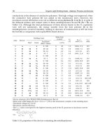
List of Tables
Table 1: Growth rates of circular features in devices with different
organic layer combinations.
69
Table 2: O 1s, N 1s, C 1s and Al 2p XPS peak binding energies
measured for Alq
3
films exposed at different time intervals.
83
Table 3: OLED with different electrode pairs and the corresponding
dark spots growth rate.
101
Table 4: Current efficiency and the corresponding operating voltage,
measured at a current density of 100 mA/cm
2
, for devices
with different thickness of Alq
3
buffer layer.
113
xiv
List of Publications
1. Investigation of the sites of dark spots in organic light-emitting devices
Yoon-Fei Liew, Hany Aziz, Nan-Xing Hu, Hardy S.O.Chan, Gu Xu, Zoran
Popovic
Applied Physics Letters, Volume 77, pp2650-2652 (2000)
2. Reduced reflectance cathode for organic light-emitting devices using
metalorganic mixtures
Hany Aziz, Yoon-Fei Liew, H. Michelle Grandin, Zoran D. Popovic
Applied Physics Letters, Volume 83, pp186-188 (2003)
3. Novel Cathode for Organic Light Emitting Devices with Reduced Optical
Reflectivity
Hany Aziz, Yoon-Fei Liew, Zoran Popovic
Proceeding of SPIE’s 48th annual meeting, Organic Light Emitting Materials
and Devices VII, San Diego, California, 3-8 August 2003Proc. SPIE Int. Soc.
Opt. Eng. 5214, pp277 (2004)
4. Effect of surface electronic properties of ITO on luminance efficiency of OLED
Furong Zhu, Hu Jian Qiao, Liew Yoon Fei, Kian, Soo Ong, Hao Xiaotao
Proc. SPIE 5277, pp163-173 (2004)
5. Effect of organic layer combination on dark spot formation in organic light
emitting devices
Yoon-Fei Liew, Furong Zhu , Soo-Jin Chua
Chemical Physics Letters, Volume 394, pp275-279 (2004)
6. Alq
3
-modified indium tin oxide for enhancing the efficiency and reliability of
organic light emitting devices
Yoon-Fei Liew, Furong Zhu, Soo-Jin Chua
Applied Physics Letters, Volume 85, pp4511-4513 (2004)
7. Fundamental of dark spot formation in organic light-emitting devices
(manuscript in preparation)
xv
Chapter 1
Introduction and Research Overview
1
1.1 Information Display
Information display is an important communication interface between man
and machine. The discovery and development of cathode-ray-tube-based television,
transmitting the full visual content of an event, have brought knowledge and
entertainment directly to the general population. The related communication and
display technologies also have used for delivering the news from around the world to
the living room. The introduction of liquid crystal displays (LCDs) enabled
information exchange applying for the portable electronics. Now the organic light-
emitting device (OLED), a novel flat panel display technology, promises to bring full
imagery and graphical content to truly convergent products, comprising video, text
and data.
OLEDs have many advantages over the existing display technologies. They
are lightweight and much thinner compared to the bulky CRT or LCD displays. They
are self–emissive with high luminous efficiency and can be operated at a few volts,
unlike CRTs that are usually operated at thousand of volts. With the advances of
chemistry and physics, OLEDs can emit light in many colors, from deep blue to
infrared. Other advances of organic thin film displays include high resolution, fast
switching speed and flexibility. However, OLEDs will have to compete with exciting,
well-established technologies like CRTs and LCDs. The market for displays is huge,
estimated to be some US$30 billion per annual [Gymer, 1996, Burrow et al. 1997],
and the lure of success is sufficient to persuade industry to invest significantly in the
development of OLEDs. Expected applications range from simple backlights for
portable battery-operated equipment, through alphanumeric displays, to complex full
2
color video screens for computer and televisions. The first commercial OLED product
was launched in 1999 by Pioneer Corporation using Kodak licensed technologies.
1.2 Display Devices
The commonly used display devices can be classified into four different types
according to their operating mechanisms, namely cathodoluminescent, non-emissive,
plasma and electroluminescent displays. Their operation mechanisms are described
briefly in the following sections.
1.2.1 Cathodoluminescent Display
The cathode ray tube (CTR) is an example of cathodoluminescent display
which is commonly used in television and computer monitor. The first CRT was
developed by Ferdinand Braun, a German scientist, in 1897. It was applied for the
television sets in the late 1940s. The mechanism of such devices is based on
cathodoluminescence, electrons are generated from an electron gun and are falled
onto phosphor screen leading to light emission. In a colored television, there are three
electron guns, each of them is controlled for emitting three primary colors, red, green,
and blue. When the operation of these three electron guns is controlled, the system
enables to produce color images for display applications.
CRTs are the most widely used display devices at present time due to its
matured technology and inexpensive price, even though the technology has been
around for nearly 70 years. However, CRT displays are very heavy and bulky. CRTs
3
require a vacuum tube and a long neck for deflecting and focusing the electron beam.
The electron optic system makes CRTs unsuitable for large flat panel displays.
Another major disadvantage of CRTs is the high operation voltage of up to 30kV. The
strong magnetic field used in the CRTs also creates harmful electromagnetic
radiation.
1.2.2 Non-emissive Display
Non-emissive displays, as the name implied, are devices that are inherently
incapable of emitting light. Liquid crystal displays, LCDs, are the most common non-
emissive display devices. Liquid crystal was first discovered in the late 19
th
century
by Friedrich Reinitzer, an Austrian botanist. The term “liquid crystal” was coined
shortly by Otto Lehmann, a German physicist. Liquid crystals are almost transparent
substances, exhibiting the properties of both solid and liquid matter. Liquid crystal
molecules tend to align parallel to each other due to their chemical structure. They
usually orient themselves randomly on a mechanically rubbed substrate, resulting in
an optical anisotropy – despite the fact that the molecules form a liquid. The
molecular orientation in liquid crystals is very sensitive to an applied electric field.
Thus a liquid crystal cell works like a tiny optically tunable shutter that can be
controlled by a locally applied electric field. The liquid crystal cell is sandwiched
between a pair of polarizers to form a single pixel. The operation of such devices is
therefore based on the presence of a separate illumination source. When electric field
is applied locally, the orientation of the liquid crystal molecules can be controlled,
leading to an optically opaque or transparent transformation. By installing a color
filter of red, green, or blue for each pixel, full color images can be displayed.
4
LCDs are currently widely used in watches, calculators, laptop computers and
television. Although lightweight, compact size with low power consumption are
considered to be their strong assets over the CRTs, LCDs have a major disadvantage
of high cost compared to CRTs. Furthermore, LCDs bear limited viewing angle and
limited operation temperature range of -20 to +50°C. These drawbacks, in addition to
their dependence on a separate illumination source, result in LCDs having limitations
in application.
“Electronic paper” is another non-emissive display technology. It offers
excellent resolution and high visual contrast display with a wide viewing angle. It
does not require an external power to retain its image, and it is lightweight,
inexpensive and remarkably flexible. This technology, being developed for
electronically configurable paper-like displays, relies on microscopic beams that
change colors in response to the charges on nearby electrodes. There are two types of
beans used: the first type is a two-tone solid bean invented by Nicholas Sheridon.
Each bean is two-toned with one half white and one half black, with opposite polarity
charges on each half, that twist around in place when respond to electrical field. The
second type of the beans, developed by Joseph Jacobson, consists of see-through
microcapsules containing charged pigment chips that move through a liquid medium
when an electrical field is applied.
This technology is being used as signboard in department store, character and
segmented displays for advertising. Commercial prototypes have been developed for
high-resolution active matrix displays including personal digital assistants (PDAs),
mobile telecommunication devices, and portable electronic books.
5
1.2.3 Plasma Displays
Plasma display panels (PDPs), similar to CRTs, also use phosphor materials
for light emission. Essentially, a PDP can be considered as a matrix of tiny fluorescent
tubes, which are controlled in a sophisticated fashion. Each cell comprises a small
capacitor with a pair of parallel electrodes and a mixture of inert gases, such as argon,
neon or xenon sealed in the cell. When a high electric field is applied between two
electrodes, electrons and ions are accelerated and bombard gas molecules to break
down gas molecules producing weakly ionized plasma. Once energized, the cells of
plasma release ultraviolet light, which then strikes and excites red, green and blue
phosphors along the face of each pixel, and visible light is emitted when the excited
molecules relax to the ground state.
Compared to conventional CRT displays, the thickness of PDPs is ~ 4 inches,
which is about one-tenth thinner than that of CRTs. A 40 inches PDP is about 67
pounds, this is about one-sixth of the weight of a typical CTR display. PDPs use over
16 million colors and have a 160° viewing angle. Because of their dependence on an
electric discharge in a gas medium, plasma displays essentially require high operating
voltage of over 100 V and demonstrate low brightness (up to 150 cd/m
2
). Another
ultimate limitation of plasma display has proved to be pixel size. At present, it is very
challenge to get pixel sizes below 0.3mm, even in the long term. A biggest obstacle
that plasma displays have to overcome is their inability to achieve a smooth ramp
from full white to dark black. Low shades of gray are particularly troublesome, a
noticeable posterised effect being present during the display of movies or other video
programming with dark scenes.
6
1.2.4 Electroluminescent (EL) Displays
The mechanism of operation of the fourth class of display devices, the
electroluminescent devices, depends on the radiative relaxation (in the form of visible
light) of excitation generated by an electrical stimulus. The EL displays can be further
classified into two classes, according to the active materials used, i.e. inorganic and
organic electroluminescent devices.
1.2.4.1 Inorganic Light Emitting Devices
There are two types of inorganic electroluminescence devices. In the first type,
light is produced by the direct recombination of electrons and holes, which move
towards each other from conduction band and valence band respectively. the carrier
are transported through a diffusion process which can be controlled by an external
applied direct current (dc) electric field. The recombination of holes and electrons in
p-n junction in inorganic light emitting diodes (LED) is one of the examples. The
electroluminescent materials are usually made of III-V semiconductor compounds.
Due to the fact that the diodes must be made of single crystal materials, which are
difficult to obtain in sizes exceeding few millimeters, the inorganic light emitting
diodes are mainly used for semiconductor lasers, indicator lights, and light sources for
optical communication. In the second type, the electroluminescence mechanism is
based on placing a doped phosphor materials, between two dielectric layers onto
which two electrodes are deposited from outside. This type of devices is also called
thin film electroluminescent device (TFEL). Electrons and holes are generated by
means of impact ionization or by quantum mechanical tunneling under the effect of a
strong externally applied high alternate current (ac) electrical field (~10
6
V/cm). The
recombination of electrons and holes take place at the dopant sites thereby producing
7
light. The phosphor materials, from the II-VI semiconductor compounds group (e.g.
ZnS), usually have a large band gap. Although such devices can be made in relatively
large size, their use is limited due to a requirement of high ac drive voltage (>100V).
In addition, most inorganic light emitting devices are linked to a narrow range of
substrates due either to stringent lattice-matching requirements, or high temperature
processes associated with semiconductor growth.
1.2.4.2 Organic Light Emitting Devices (OLEDs)
Organic semiconductor based light emitting device is the most recent class of
display devices. The device structure and operation mechanism are quite similar to the
first type of inorganic LED, except that the active electroluminescent materials are
organic semiconductors. In the most basic device structure, a thin layer of an organic
electroluminescence material (50-100nm) is sandwiched between two metal
electrodes in which at least one is transparent. Figure 1.1 shows a schematic diagram
of a typical OLED structure. Under the influence of an externally applied dc field,
electrons and holes are injected from the opposite electrodes, and transported towards
each other to form electron-hole pair called exciton. Light is produced and emitted
through the relaxation of the exciton process from the transparent electrode side.
Obtaining electroluminescence in an OLED required placing the organic
electroluminescent materials between two conducting electrodes with different work
functions. The difference in work function is required for the efficient injection of
electrons and holes. When an electric field is applied, electrons are injected from
electrode with lower work function, called cathode, into the conduction band of the
organic materials, while holes are injected from electrode with higher work function,
8
cathode
organic stack
anode (ITO)
glass
LIGHT
Figure 1.1: A cross sectional view of a typical OLED.
9