Patterned ferromagnetic meso and nano structures
Bạn đang xem bản rút gọn của tài liệu. Xem và tải ngay bản đầy đủ của tài liệu tại đây (7.75 MB, 190 trang )
PATTERNED FERROMAGNETIC MESO AND NANO STRUCTURES
GOOLAUP SARJOOSING
NATIONAL UNIVERSITY OF SINGAPORE
2007
PATTERNED FERROMAGNETIC MESO AND NANO STRUCTURES
GOOLAUP SARJOOSING
(B. Eng(Hons.), NUS)
A THESIS SUBMITTED
FOR THE DEGREE OF DOCTOR OF PHILOSOPHY
DEPARTMENT OF ELECTRICAL AND COMPUTER ENGINEERING
NATIONAL UNIVERSITY OF SINGAPORE
2007
i
Acknowledgements
First and foremost, I would not be writing these words, had I not taken the magnetic
course, taught by Associate Professor Adekunle Adeyeye, in the final year of my
undergraduate degree. I would like to sincerely thank my supervisor Associate Prof
Adekunle Adeyeye for giving me the opportunity to join his group and to work on the
exciting topic of magnetism. He is someone who is bubbling with a contagious
enthusiasm for research. His support, advice and working attitude helped me a lot in
carrying out my research. I am also grateful to him for believing in me and giving me
the freedom and support to pursue my own avenues in research.
I would like to give special thanks to Mr Navab Singh from the Institute of
Microelectronics for providing me with the deep ultra violet resist patterns used in this
thesis. I would also like to thank Dr Wang Chen Chen and Ms. Jain Shika for reading
through this thesis.
It has been a delight to work with the current and past members of my research
group: Mr Tripathy Debashish who has been a great friend and taught me a lot about
half-metals! and Mr Chui Kiam Ming for forcing me to speak French. Also, I would
like to thank my friends in the lab for making it a fun place to work; Mr Mambakkan
Sreenivasen for always having some tid-bits to help stave away the hunger pangs at
night and Mr. Cheng Xingzhi, for trying to teach me Chinese.
I would like to thank my mum and dad for supporting me to pursue the PhD
degree and pretending to understanding magnetism when I explained it to them. I am
also grateful to my “little” brother, Avinash and my “twin” sister, Venita for their
support and encouragement. Lastly, but not least, I would like to thank my flat mate
Alex for putting up with me for the past 4 years!
ii
Table of Contents
Acknowledgements
i
Table of Contents ii
Summary
vi
List of Tables
viii
List of Figures
ix
List of Symbols and Abbreviations
xvi
Statement of Originality
xviii
Chapter 1 Introduction
1.1 Why Meso-Nano Magnets? 1
1.1.1 Fundamental Perspective 1
1.2.1 Application Perspective 2
1.2 Challenges in the Fabrication of Meso-Nano Magnets 4
1.3 Focus of this Thesis 5
1.4 Organization of this Thesis 6
References 8
Chapter 2 Theoretical Background
2.1 Introduction 12
2.2 Magnetic Energies 12
2.2.1 Exchange Energy 13
2.2.2 Zeeman Energy 13
2.2.3 Magnetic Anisotropy Energy 14
2.2.4 Magnetostatic Energy 15
2.3 Magnetization Reversal Mechanism 16
2.3.1 Coherent Rotation 17
2.3.2 Curling 20
2.4 Coupling in Multilayer Films 22
2.4.1 Pinhole Coupling 22
Table of Contents
iii
2.4.2 RKKY Coupling 23
2.4.3 Néel Coupling 25
2.4.4 Interlayer Magnetostatic Coupling 26
2.5 Magneto Resistance Effect
2.5.1 Anisotropic Magnetoresistance
2.5.2 Giant Magnetoresistance/Spin Valve
26
27
28
2.6 Summary 29
References 30
Chapter 3 Experimental Techniques
3.1 Introduction 34
3.2 Fabrication Techniques 34
3.2.1 KrF Deep Ultra Violet Lithography 36
3.2.2 Deposition Techniques 38
3.2.2.1 Evaporation 38
3.2.2.2 Sputtering 40
3.2.2.3 Lift-off 41
3.3 Characterization Techniques 41
3.3.1 Scanning Electron Microscope 44
3.3.2 Scanning Probe Microscope 43
3.3.2.1 Atomic Force Microscope 43
3.3.2.2 Magnetic Force Microscope 44
3.3.3 Vibrating Sample Magnetometer 46
3.3.4 Magnetoresistance Measurement 48
3.4 Summary 49
References 51
Chapter 4 Magnetization Reversal in Ni
80
Fe
20
Nanowires
4.1 Introduction 53
4.2 Sample Fabrication 54
4.3 Shape Anisotropy 56
4.4 Effect of Ni
80
Fe
20
wire thickness 58
4.4.1 Fields Applied Along Easy Axis 58
4.4.2 Fields Applied Along Hard Axis 61
Table of Contents
iv
4.5 Field Orientation Dependent Measurements 67
4.6 Angular Coercivity Variations 69
4.6.1 Modeling of curling mode of rotation 71
4.7 Magnetoresistance Measurement 73
4.8 Thickness Dependent MR Measurements 76
4.9 Switching Field Variations 78
4.10 Summary 80
References 81
Chapter 5 Dipolar Coupling in Pseudo Spin Valve
Nanowires
5.1 Introduction 84
5.2 Sample Fabrication 85
5.3 Magnetic Properties of Pseudo-Spin Valve Nanowires 86
5.4 Effect of Cu thickness on Dipolar Coupling 89
5.5 Differential Magnetization Loops 94
5.6 Minor Hysteresis Loop Measurement 97
5.7 Interaction Field 100
5.8 Summary 102
References 104
Chapter 6 Magnetization Switching in Alternating Width
Nanowires
6.1 Introduction 106
6.2 Sample Fabrication 107
6.3 Reversal Process in Alternating Width Nanowires 108
6.3.1 Fields Applied Along Easy Axis 109
6.3.2 Schematic Magnetic States 112
6.3.3 Fields Applied Along the Hard Axis 113
6.4 Effect of Ni
80
Fe
20
Wire Thickness 114
6.4.1 Fields Applied Along Easy Axis 115
6.4.2 Fields Applied Along Hard Axis 118
6.5 Dipolar Field in Alternating Width Nanowires 121
6.6 Magnetization Reversal Mechanisms 124
Table of Contents
v
6.6.1 Reversal Modes of w
1
Nanowires 125
6.6.2 Reversal Modes of w
2
Nanowires 127
6.7 Summary 128
References 130
Chapter 7 Spin State Evolution in Diamond-Shaped
Nanomagnets
7.1 Introduction 132
7.2 Sample Fabrication 133
7.3 Single layer Ni
80
Fe
20
Nanomagnets 134
7.4 Simulation For Reversal Along Major Axis 136
7.5 Remanent Spin State Configuration 141
7.6 Single layer Co Nanomagnets 142
7.7 Comparative Study of Thickness Dependence 143
7.8 Trilayer Nanomagnets 146
7.9 3-D Simulation for Reversal Along Major Axis 151
7.10 Remanent State of Trilayer Nanomagnet 154
7.11 Interlayer Coupling 156
7.12 Summary 159
References 160
Chapter 8 Conclusion and Outlook
162
Appendix
List of Publications 167
vi
Summary
The magnetization reversal process in patterned single and multilayer nanomagnets has
been systematically studied, as a function of various geometrical parameters, using a
combination of characterization techniques and simulation tools. Ordered
homogeneous nanomagnets were fabricated over a large area (4×4 mm
2
) using deep
ultra violet lithography at 248 nm exposure wavelength and lift-off technique, allowing
for characterization of magnetic properties using conventional magnetometers.
Firstly, the magnetization reversal mechanism in Ni
80
Fe
20
nanowire arrays as a
function of wire thickness was systematically investigated. It was observed that for
fields applied along the wire easy axis, a non-monotonic variation of the coercivity
was observed, due to the different mechanisms of magnetization reversal dominating
the switching process in the nanowire arrays. The angular dependence of coercivity
was used to map the reversal mechanism in the nanowires. A cross-over from coherent
rotation to curling mode of reversal was observed for thickness to width ratio > 0.5.
The understanding of the reversal process was validated using theoretical modeling.
Secondly, the question of how the magnetostatic interaction affects the reversal
process in pseudo-spin valve (PSV) nanowire arrays was addressed. Closely packed
and isolated homogeneous width Ni
80
Fe
20
(10 nm)/Cu(t
Cu
)/Ni
80
Fe
20
(80 nm) PSV
nanowires with varied Cu spacer layer thickness were studied. Marked changes in the
magnetization reversal process were observed, as the Cu spacer layer thickness
becomes comparable to the edge-to-edge spacing of the closely packed nanowires.
This was attributed to the competition between the dipolar coupling in the neighboring
nanowires and the interlayer magnetostatic coupling between the 10 nm and 80 nm
Summary
vii
Ni
80
Fe
20
layers. Minor loop revealed that the 10 nm Ni
80
Fe
20
layer in the closely
packed PSV nanowire experienced a larger interaction field as compared to the
isolated nanowires, leading to a smaller region of anti-parallel alignment in the closely
packed nanowires.
Thirdly, by exploiting the width dependence of coercivity in nanowires, it has
been shown that complex nanowire arrays with unique magnetic properties can be
engineered. Alternating width nanowires consisting of two sets of Ni
80
Fe
20
nanowires
differentiated by their width, which are alternated in an array, were fabricated and
systematically studied. The magnetization reversal process in the alternating width
nanowire arrays was found to be markedly sensitive to the Ni
80
Fe
20
wire thickness and
differential width, ∆w, between the two sets of nanowires. Minor M-H loop
measurements, revealed that the interaction field, was strongly dependent on the
individual wire width constituting the array.
Finally, a comprehensive study of the spin state evolution in diamond-shaped
nanomagnets was conducted. The effect of film composition and thickness on the
magnetic properties of the nanomagnets was systematically investigated. An evolution
from coherent rotation to vortex mediated reversal was observed as the film thickness
was increased. The onset of the vortex state was found to be strongly dependent on the
film thickness and composition. By stacking layers with different modes of reversal,
PSV nanomagnets with unique properties were fabricated. The understanding of the
reversal process was aided using 2-D and 3-D micromagnetic simulations. MFM
imaging was used to confirm the magnetic spin states of the nanomagnets.
viii
List of Tables
Table 5.1 Effective Coercivity and interaction field for wire A, s = 35 nm
and wire B, s = 185 nm as a function of the Cu spacer layer
thickness
102
Table 6.1 Effective Coercivity and interaction field for alternating width
nanowire arrays as a function of the Cu spacer layer thickness
123
ix
List of Figures
Figure 2.1 Schematic illustration of the spin configuration and the
corresponding exchange energy level.
13
Figure 2.2 Illustration of the formation of flux closure formation in a
magnetic bar to reduce the high magnetostatic energy due to
surface charges at the edges.
15
Figure 2.3 Uniformly magnetized prolate ellipsoid with the magnetization at
an angle α from the semi-major axis.
16
Figure 2.4 Schematic illustration of the spin rotation during the coherent
reversal mode in a prolate spheriod.
17
Figure 2.5 Co-ordinate system for prolate spheroid 18
Figure 2.6 Calculated angular dependence of the reduced switching field and
coercivity for coherent rotation model.
20
Figure 2.7 Schematic illustration of the magnetic dipole during the curling
mode reversal in an ellipsoid.
21
Figure 2.8 Configuration of the magnetization in a direct exchange coupled
film
23
Figure 2.9 RKKY Coupling strength J as a function of the spacer layer
thickness
24
Figure 2.10 Orange peel coupling from correlated roughness. The pluses and
minuses are the effective magnetic charges. The schematic
shows the fringing fields in the presence of two correlated
roughness for the case of parallel magnetization
25
Figure 2.11 Charge distribution and magnetostatic energy levels for the
parallel and anti-parallel alignment of the FM layers in a trilayer
structure
26
Figure 2.12
Schematic Illustration of the AMR effect for the simplest case of
uniform magnetization
28
List of Figures
x
Figure 2.13 Schematic of a simple Spin Valve Structure 29
Figure 3.1 Schematic of the flow of the fabrication process for the
nanomagnet arrays
35
Figure 3.2 Illustration of phase shift mask for a typical DUV lithography
process
37
Figure 3.3 Schematic of the electron beam and thermal evaporation system 39
Figure 3.4 Schematic of the in-house designed sample holder 40
Figure 3.5 Illustration of film growth via sputtering 41
Figure 3.6 Schematic of the sample-electron interaction 42
Figure 3.7 Schematic of the typical AFM Measurement 44
Figure 3.8 Schematic diagram of the VSM setup 47
Figure 3.9 Schematic illustration of the fully automated in-house developed
MR measurement setup.
49
Figure 4.1 SEM Micrograph showing the lateral dimensions of the nanowire
arrays, with width 185 nm and edge-to-edge spacing of 35 nm.
55
Figure 4.2 M-H loops for 20 nm thick Ni
80
Fe
20
nanowire arrays, w = 185 nm
and s = 35 nm, with fields applied along (a) = 0° and (b) =
90°, with respect to the long axis.
57
Figure 4.3 M-H loops for 20 nm thick Ni
80
Fe
20
reference film with fields
applied along (a) = 0° and (b) = 90°.
58
Figure 4.4 Representative M-H loops for nanowire arrays, of width = 185
nm and edge-to-edge spacing = 35 nm, with field applied along
the easy axis for different Ni
80
Fe
20
wire thicknesses.
59
Figure 4.5 Easy Axis coercivity of the Ni
80
Fe
20
nanowires, of width = 185
nm and edge-to-edge spacing = 35 nm, as a function of
thickness/width ratio. The dotted line is a visual guide.
61
Figure 4.6 Representative M-H loops for nanowire arrays of w = 185 nm
and s = 35 nm, with field applied along the hard axis for different
Ni
80
Fe
20
wire thicknesses.
62
List of Figures
xi
Figure 4.7 Hard axis saturation field as a function of Ni
80
Fe
20
film thickness
of the nanowires with w = 185 nm and s = 35 nm.
63
Figure 4.8 SEM Micrograph of the isolated nanowire arrays, with width 185
nm and edge-to-edge spacing of 185 nm.
65
Figure 4.9 Representative M-H loops for nanowire arrays, of width = 185
nm and edge-to-edge spacing = 185 nm, with field applied along
the easy (θ = 0°) and hard (θ = 90°) axis for different Ni
80
Fe
20
wire thicknesses.
66
Figure 4.10 Representative M-H loops for nanowire arrays, of w = 185 nm
and s = 35 nm, for different Ni
80
Fe
20
film thicknesses with fields
applied along (a-e) θ = 30° and (f-j) θ = 60°.
68
Figure 4.11 Coercivity as a function of the field orientation with respect to
the nanowire (w = 185 nm and s = 35 nm) axis, for Ni
80
Fe
20
wire
thickness ranging from 10nm to 150nm.
70
Figure 4.12 Angular variation of coercivity together with theoretical
prediction based on curling magnetization for (a) 120 nm, (b) 150
nm and (c) 180 nm, for nanowires with w = 185 nm and s = 35
nm.
73
Figure 4.13 MR response for 20 nm thick Ni
80
Fe
20
nanowire arrays (w = 185
nm and s = 35 nm) with fields applied along (a) = 15° and (b)
= 90°, with respect to the long axis. (c) Schematic diagram of the
magnetic reversal process for 20 nm thick Ni
80
Fe
20
nanowire with
fields along = 15°.
75
Figure 4.14 MR response for nanowire arrays, with w = 185 nm and s = 35
nm, for fields applied along = 90°, with respect to the long axis,
for different Ni
80
Fe
20
film thicknesses.
77
Figure 4.15 Switching field as a function of the field orientation with respect
to the wire axis, for Ni
80
Fe
20
film thickness of (a) 20nm, (b)
80nm and (c) 120nm, for nanowire with w = 185 nm and s = 35
nm (the dashed line is the theoretical prediction using curling
mode of reversal).
79
List of Figures
xii
Figure 5.1 Scanning Electron Micrograph of Ni
80
Fe
20
(10 nm)/Cu(35
nm)/Ni
80
Fe
20
(80 nm)
spin-valve nanowire arrays with width 185
nm, (a) edge-to-edge spacing = 35 nm and (b) edge-to-edge
spacing = 185 nm; (c) schematic representation of the spin valve
nanowires.
86
Figure 5.2 M-H Loops for Ni
80
Fe
20
(10 nm)/Cu(10 nm)/Ni
80
Fe
20
(80 nm)
nanowire arrays with fields applied along the wire axis for (a)
closely packed, s= 35 nm wire A and (b) isolated, s = 185 nm,
wire B.
87
Figure 5.3 Representative M-H loops for both the closely packed and
isolated nanowire arrays with Ni
80
Fe
20
(10 nm)/Cu(t
Cu
nm)/Ni
80
Fe
20
(80 nm)
film as a function of the Cu spacer layer
thickness, t
Cu
.
91
Figure 5.4 Differentiated M-H loops for the isolated and closely packed
PSV nanowire arrays with (a) t
Cu
= 20nm and (b) t
Cu
= 35nm.
95
Figure 5.5 Schematic representative of the different states for
Ni
80
Fe
20
(10nm)/Cu(35nm)/Ni
80
Fe
20
(80nm) spin-valve nanowire
array with width 185nm and edge-to-edge spacing = 35nm.
97
Figure 5.6 Representative M-H loops and minor loops for Ni
80
Fe
20
(10
nm)/Cu(t
Cu
nm)/Ni
80
Fe
20
(80 nm)
spin-valve nanowire arrays with
t
Cu
= 20 nm; (a) wire A, s = 35nm and (b) wire B, s = 185nm, and
t
Cu
= 35 nm; (c) wire A, s = 35nm and (d) wire B, s = 185nm, as a
function of the reverse field, H
m.
98
Figure 5.7 Representative M-H loops and minor loops for Ni
80
Fe
20
(10
nm)/Cu(20 nm)/Ni
80
Fe
20
(80 nm)
isolated spin-valve nanowire
arrays B, with s = 185nm (a) full M-H loop and minor loop for
H
m
= -100 Oe and (b) normalized minor loop
.
101
List of Figures
xiii
Figure 6.1 Scanning Electron Micrograph of 40nm Ni
80
Fe
20
thick;
alternating nanowire arrays with (a) homogeneous width
nanowire array, ∆w = 0 (w
1
= 330nm; w
2
= 330nm) (b) ∆w =
200nm (w
1
= 330nm; w
2
= 530nm), (c) ∆w = 570nm (w
1
=
330nm; w
2
= 900nm). The inset shows the respective images at
higher magnification. The edge-to-edge spacing for all the
nanowire arrays is maintained at 70nm.
108
Figure 6.2 Magnetic hysteresis and l Differentiated M-H loops for nanowire
arrays 70nm thick Ni
80
Fe
20
film withfields applied along the long
axis (θ = 0°); (a) ∆w = 0 (w
1
= 330nm; w
2
= 330nm) (b) ∆w =
200nm (w
1
= 330nm; w
2
= 530nm), (c) ∆w = 570nm (w
1
=
330nm; w
2
= 900nm)
110
Figure 6.3 Schematic representation of the different states of the 70nm thick
Ni
80
Fe
20
alternating width nanowires.
113
Figure 6.4 Magnetic Hysteresis loops for 70nm thick Ni
80
Fe
20
nanowire
arrays with fields applied along θ = 90°.
114
Figure 6.5 Representative M-H loops for the nanowire arrays, with ∆w = 0,
200 nm, and 570 nm as a function of the Ni
80
Fe
20
film thickness
for fields applied along θ = 0°.
116
Figure 6.6 Representative M-H loops for the nanowire arrays, with ∆w = 0,
200 nm, and 570 nm as a function of the Ni
80
Fe
20
film thickness
for fields applied along θ = 90°.
119
Figure 6.7 Hard Axis Saturation field for nanowire arrays, with ∆w = 0, 200
nm, and 570 nm as a function of the Ni
80
Fe
20
film thickness.
121
Figure 6.8 Representative M-H loops and minor loops for 80 nm Ni
80
Fe
20
alternating nanowire arrays with (a) ∆w = 200nm, (b) ∆w =
570nm, as a function of the reverse field, H
m.
122
Figure 6.9 Representative coercive field of the w
1
nanowire, as a function of
the field orientation with respect to the wire axis for wire arrays
with ∆w = 0, ∆w = 200 nm and ∆w = 570nm, for Ni
80
Fe
20
film
thickness 20nm, 40nm and 80nm.
126
List of Figures
xiv
Figure 6.10 Representative coercive field of the w
2
nanowire, as a function of
the field orientation with respect to the wire axis for alternating
wire arrays with ∆w = 200 nm and ∆w = 570nm, for Ni
80
Fe
20
film thickness 20nm, 40nm and 80nm.
128
Figure 7.1 Scanning Electron Micrograph of diamond-shaped
Ni
80
Fe
20
(10nm)/Cu(2 nm)/Ni
80
Fe
20
(40 nm)
tri-layer structure.
The inset shows the nanomagnets at a larger magnification.
134
Figure 7.2 Magnetic hysteresis loops for 60 nm Ni
80
Fe
20
diamond-shaped
nanomagnet for field orientation (a) θ = 0°, (b) θ = 90°. The
respective insets are the corresponding M-H loops of the
unpatterned reference film.
135
Figure 7.3 Magnetization loop obtained from micromagnetic simulation of a
4×4 array 60 nm thick Ni
80
Fe
20
diamond shaped structure for
field applied along θ = 0°, for field swept from positive to
negative saturation (
) and from negative saturation to
positive (
). The inset shows the schematic diagram of the
model used in OOMMF.
137
Figure 7.4 Micromagnetic simulation of the magnetic spin states of the
central region of a 4x4 array of 60 nm thick Ni
80
Fe
20
diamond-
shaped nanomagnet.
139
Figure 7.5 MFM image of 60 nm Ni
80
Fe
20
thick diamond-shaped
nanomagnet at remanence.
141
Figure 7.6 Magnetic hysteresis loops for 60 nm Co Diamond-shaped
nanomagnet for field orientation (a) θ = 0°, (b) θ = 90°. The
respective insets are the corresponding M-H loops of the
unpatterned reference film.
142
Figure 7.7 Representative Magnetic hysteresis loops for Ni
80
Fe
20
and Co
Diamond-shaped nanomagnet for different film thicknesses with
field applied along θ = 0°.
144
List of Figures
xv
Figure 7.8
Magnetization loops for fields applied along the major axis (θ =
0°) for Ni
80
Fe
20
(10nm)/Cu(2nm)/Ni
80
Fe
20
(40nm) diamond-
shaped nanomagnets.
147
Figure 7.9 Hysteresis loop and minor loop of an array of the
Ni
80
Fe
20
(10nm)/Cu(2nm)/Ni
80
Fe
20
(40nm) thick diamond-shaped
Ni
80
Fe
20
nanomagnets, for different reversing field, H
m
applied
along the major axis
.
149
Figure 7.10 Calculated Magnetization loop obtained from 3-D OOMMF
simulation for fields applied along the major axis (y-direction)
for diamond-shaped nanoelements with
Ni
80
Fe
20
(10nm)/Cu(2nm)/Ni
80
Fe
20
(40nm) pseudo spin-valve.
152
Figure 7.11 Micromagnetic simulation of the magnetic spin states of a single
diamond-shaped tri-layer nanomagnet.
153
Figure 7.12 MFM image of the Ni
80
Fe
20
(10nm)/Cu(2nm)/Ni
80
Fe
20
(40nm)
thick diamond-shaped Ni
80
Fe
20
nanomagnet at remanent state.
The dark circles represent structures with the “S-spin”
configuration.
155
Figure 7.13 M-H loops of Ni
80
Fe
20
(10 nm)/Cu(t
Cu
nm)/Ni
80
Fe
20
(40 nm)
Diamond-shaped nanomagnets, as function of Cu spacer layer
thickness for fields applied along θ = 0°.
157
Figure 7.14 Nucleation field, H
nT
of the Ni
80
Fe
20
(10 nm)/Cu(t
Cu
nm)/Ni
80
Fe
20
(40 nm) nanomagnets, as a function of field
orientation, θ, for different Cu spacer layer thicknesses.
158
Figure 8.1 Figure 8.1: Schematic illustration for conventional MR
measurement
165
Figure 8.2 Illustration of large area nanomagnets with thin film coating, (a)
dot arrays and (b) wire arrays
166
xvi
List of Symbols and Abbreviations
2-D Two Dimensional
3-D Three Dimensional
AFM Atomic force microscope
AMR Anisotropic magnetoresistance
ALT PSM Alternating phase shift mask
Au Gold
BARC Bottom anti-reflection coating
BNC Bayonet Neill Concelman
Co Cobalt
Cr Chromium
Cu Copper
DC Direct current
DUV Deep ultraviolet
EBL Electron beam lithography
FM Ferromagnetic
H
a
Annihilation field
H
n
Nucleation Field
MFM Magnetic force microscopy
MR Magnetoresistance
MRAM Magnetic Random Access Memory
NA Numerical aperture
List of Symbols and Abbreviations
xvii
OOMMF Object Oriented MicroMagnetic Framework
PSV Pseudo spin-valve
RKKY Ruderman-Kittel-Kasuya-Yosida
SEM Scanning Electron Microscope
SFD Switching field distribution
SNR Signal to noise ratio
SPM Scanning Probe Microscopy
VSM Vibrating Sample Magnetometer
XRL X-ray lithography
xviii
Statement of Originality
The author claims the following aspects of the thesis to be original contributions to
knowledge.
A systematic study of the magnetization reversal process in Ni
80
Fe
20
nanowires
as a function of various geometrical parameters and established a cross-over
from coherent rotation to curling mode when the thickness to width ratio is
greater than 0.5. The experimental results were validated using theoretical
model.
[1] S. Goolaup, N. Singh, A. O. Adeyeye, V. Ng and M. B. A. Jalil, Eur.
Phys. J. B, 44, 259 (2005)
[2] S. Goolaup, N. Singh and A. O. Adeyeye, IEEE Trans. Nano., 4 ,523
(2005)
[3] S. Goolaup, A. O. Adeyeye and N. Singh, Thin Solid Films, 505, 29
(2006)
• Detailed and systematic investigation of the effect of dipolar coupling in
pseudo-spin valve nanowires. Marked changes were observed when the spacer
layer thickness becomes comparable to the edge-to-edge spacing of the
nanowires.
[4] S. Goolaup, A. O. Adeyeye and N. Singh, J. Appl. Phys., 100, 114301
(2006).
Statement of Originality
xix
• Design, fabrication and characterization of alternating width nanowires with
novel magnetic properties.
[5] S. Goolaup, A. O. Adeyeye, N. Singh, G. Gubbiotti, Phys. Rev. B., 75,
144430 (2007)
• A comprehensive investigation of the magnetization reversal in diamond-
shaped nanomagnet. Established the transition region from coherent to vortex
mediated reversal as a function of both the film thickness and composition.
Novel structures with unique magnetic properties were fabricated by combing
layers with different reversal modes into a
pseudo spin-valve structure.
[6] S. Goolaup, A. O. Adeyeye and N. Singh, J. Phys. D: Appl. Phys., 38,
2749 (2005)
[7] S. Goolaup, A. O. Adeyeye and N. Singh, J. Appl. Phys., 98, 084318
(2005)
[8] S. Goolaup, A. O. Adeyeye and N. Singh, Phys. Rev. B., 73, 104444
(2006).
1
I am always doing that which I can not do, in order that I may learn how to do it. Pablo
Picasso
Introduction
1.1 Why Meso-Nano magnets?
In recent years, with the advancement in lithographic and other controlled
nanofabrication techniques, the exploration of magnetism in arrays of laterally
controlled magnetic structures down to the nanometer scale is now possible. Aided
with the increase in the processing power of computers, the micromagnetics of
nanomagnets are now solvable, thus allowing for direct comparison with experimental
observations. There is a huge interest in the study of deep sub-micron to nanoscale
(meso-nano) magnets from both a fundamental and application perspective.
1.1.1 Fundamental Perspective
From a fundamental viewpoint, novel properties are expected when the lateral
dimensions of the magnets are made comparable or smaller than certain characteristic
length scales such as spin diffusion length (e.g for Ni at 4.2K, l
sd
≈ 21 nm [1]), carrier
mean free path (e.g CoFeB at 4.2K, l = 70 nm [2]) and domain wall width (e.g for Fe,
l
d
≈ 39.5 nm [3]). The magnetization state of a bulk magnetic material is usually
magnetically divided into domains and the exact domain configuration is unpredictable
Chapter 1
Introduction
2
due to the many regions of energy minimum. When the magnetic material is patterned
down to the meso-nano scale; the number, size and orientation of the domain becomes
well defined and predictable. Brown’s fundamental theorem states that due to the
competition between the magnetostatic, exchange and anisotropy energies, magnetic
domain formation should be completely suppressed in very small particles leading to
nanomagnets behaving as a single giant spin [4]. This lateral confinement of the
magnets, leads to both new magnetization reversal behaviors and also novel transport
properties in the structures.
For a conventional magnetic material, the anisotropy arises from the
configuration of the electronic Fermi surface. In meso-nano magnets, the anisotropy
depends on the interplay between the band structure of the parent material and the
shape of the meso-nano magnets. The overall anisotropy (magnetization direction) can
be engineered by tailoring the shape and size of the meso-nano magnets. As the
magnetic material is patterned down to the meso-nano scale regime, for ordered arrays
of nanomagnets, the interaction between the elements may lead to new collective
magnetic properties, which is different from the isolated elements [5-8]. Also, the
ordered arrays of nanomagnets are a well suited system for testing micromagnetics and
exploring new physics.
1.1.2 Application
From an application perspective, meso-nano magnets are the basic building blocks for
future spintronics devices. With the increase in demand for storage capacity, the
current conventional recording medias are fast approaching their maximum recording
density due to the onset of the superparamagnetic effect, where the data is vulnerable
Introduction
3
to thermal fluctuations [9-11]. Patterned media consisting of arrays of identical
nanomagnets is viewed as the next generation candidate for ultra-high density storage
[12-15]. In patterned media, each bit is stored in an individual nanomagnet, promising
storage densities of at least 1 Terabit/in
2
.
The spin-dependent transport properties of nanomagnets are also attracting a lot
of attention due to the novel idea of using the “spin” angular momentum of electron to
operate future devices [16-20]. Magnetic Random Access Memory (MRAM) is one
such device that exploits the “spin” of electron, for storing information. MRAM
consists of nanomagnets comprising of two magnetic layers with different switching
fields. Changes between the "1" and "0" states are accomplished by altering the spin
of localized electrons on one of the magnetic layers using spin transfer [16-20]. These
states are sensed by measuring the resistance of the element. The non-volatility of
MRAM, the ability to retain data when switched off, allows the prospect of boot-free
computers. MRAM also offers the promise for smaller, faster, cheaper, and less power
hungry memories [21-24].
Recently, it has been postulated that the scope of spintronics could be greatly
expanded if in addition to data storage, the nanomagnetic bits could interact to perform
some kind of computation, resulting in a completely magnetic computer. A processing
mechanism based on magnetism, in which networks of interacting mesomagnets have
been used to perform logic operations and propagate information has been reported [25,
26]. Allwood et al [27, 28], demonstrated that similar logic operations may be
performed in an all-metallic submicron magnetic structure. These kinds of systems
promise to offer a thousand-fold increase in integration density and hundredfold
reduction in power dissipation as compared to the current micro-electronic technology.
Introduction
4
1.2 Challenges in the Fabrication of Meso-Nano Magnets
The ability to characterize nanostructures and extract quantitative information about
the magnetic properties and the reversal mechanisms is very crucial in the study of
nanomagnets. As the characterization of a single nanostructure is extremely difficult,
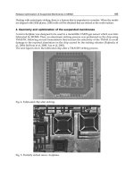
it is highly desirable to fabricate nanostructures over a macroscopic area. This will
allow the measurement of the magnetic properties using conventional magnetometric
techniques such as vibrating sample magnetometer. Thus, the major challenge lies in
the fabrication of large area arrays of homogeneous nanomagnets. Various methods
for synthesizing nanomagnets have been developed in the last few years; electron
beam lithography [29-32], focused ion beam etching [33], X-ray lithography [34-36],
nanoimprint lithography [37-39] and nanotemplating method [40-43].
Electron beam lithography (EBL) together with deposition and lift-off
technique is widely used for the fabrication of magnetic nanostructures. EBL allows
for the direct writing of the nanostructures onto the resist, enabling the patterning of
patterns with arbitrary shapes and array configuration [30-32, 44]. The major
drawback of EBL is the serial nature of the patterning process. As such the fabrication
large area of nanostructures is time consuming and costly. Also, thin resists are used
to improve the resolution of the structures as such high aspect ratio nanomagnets
cannot be fabricated. EBL also suffers from the proximity effect, which prevents the
patterning of closely packed nanostructures.
X-ray lithography (XRL) is an alternative to EBL, allowing for the fabrication
of large area fabrication of nanomagnets. The short wavelength of the X-ray
overcomes the diffraction limits in resolution as suffered by conventional optical