Low temperature high performance indium tin oxide films and applications
Bạn đang xem bản rút gọn của tài liệu. Xem và tải ngay bản đầy đủ của tài liệu tại đây (2.12 MB, 157 trang )
LOW TEMPERATURE HIGH PERFORMANCE INDIUM
TIN OXIDE FILMS AND APPLICATIONS
HU JIANQIAO
(B.Sc., Beijing Normal University)
A THESIS SUBMITTED
FOR THE DEGREE OF DOCTOR OF PHILOSOPHY
DEPARTMENT OF MATERIALS SCIENCE
NATIONAL UNIVERSITY OF SINGAPORE
2004
ACKNOWLEDGEMENTS
First of all, I would like to thank my supervisors, Dr. Zhu Furong (IMRE) and
Associate Professor Gong Hao (Department of Materials Science, NUS). Working with
both of my supervisors proved to be successful and productive. I am indebted to Dr Zhu
for his continuous guidance, constructive comments, technical and moral support during
the course of this study. My thinking has been immeasurably sharpened by having so
many invaluable discussions with Dr Zhu. I am grateful to Professor Gong for
providing excellent supervision throughout the whole project. His support and
invaluable advice were greatly appreciated. It’s been my good fortune to be their
student. I can never say it enough: Thank you so much for everything.
This project would not have been possible without much assistance from
scientists at IMRE as well as excellent research environment provided by IMRE. I
would like to thank a few more special persons here. Dr Pan Jisheng, for technical
assistance on XPS measurements and data interpretation, Dr Zhang Jian, for his help
with ITO-QCM sensor fabrication and testing. I would also like to thank research staff
and students from Dr Zhu’s group, Dr Hao Xiaotao, Mr Ong Kian Soo, Ms Tan Li Wei,
Ms Li Yanqing and Mr Roshan Shrestha, for their patient and generous technical
assistance. It has been a pleasure and a privilege for me to work with them.
I am very grateful to my mum and dad for their consistent encouragement,
support and understanding during my study in Singapore. Both of them have guided and
I
changed my life with brighter and prosperous future. Without them, I will not be what I
am today. I love them all.
Completing this PhD study has been the most challenging time in my life. Many
thanks to my best friends, for cheering me up when I was depressed.
My postgraduate study was fully supported by IMRE’s Postgraduate Research
Scholarship and IMRE Top-Up Awards.
II
TABLE OF CONTENTS
Acknowledgement……………………………… …… ………… …………….………I
Table of contents………………….……… …….…….……………………… …… III
Summary………………………………… ……………………… ……… …….….VI
List of tables…………………………………… ………………………………… VIII
List of figures…………… ……………………… …….………………….…IX
Abbreviations………………………………… ………….………………………….XIII
List of publications………………………………… ………….……………………XV
Chapter 1 Introduction………………………………… …………………………….1
References……………………………………………………….… …………………….7
Chapter 2 Theory and literature Review…………………… ….…………… ………9
2.1 Band structure of ITO.…….…………….…………………………………………….9
2.2 Electrical properties of ITO…………………………………………………….……12
2.2.1
Carrier concentration…… ……………………………………………………….13
2.2.2 Carrier mobility…………………………….…….………………………………… 17
2.3 Optical properties of ITO…… ………………… …….………………… ……… 19
2.4 Surface electronic properties of ITO…………………………………………………21
2.5 Growth of ITO films
………………………………………………………………………… 25
References……………………………………………………………………………… 32
Chapter 3 Experimental ……………………………………………………………….37
III
3.1 Thin film and device fabrication system …………………………………………….37
3.2 Film characterization techniques……………………….…… …… ………… …38
3.2.1 Four-point probe………….……………………………………………………… 38
3.2.2 Hall effect………………………………………………………………………… 39
3.2.3 UV-visible spectrophotometer…………………………………………………… 41
3.2.4 Photoelectron spectroscopy………………………………………………….…….42
3.3 Device fabrication………………………… ……………………………………… 45
3.3.1 Fabrication of OLEDs……………………………………………………….…… 45
3.3.2 Fabrication of ITO-QCM… ……….………………… ………… …………… 49
References……………………………………………… ……………………….…… 52
Chapter 4 Properties of low temperature ITO and OLED application …………….53
4.1 Preparation of ITO films…………………………………………………………… 55
4.2 Electrical and optical properties………………………………………… …… … 56
4.3 Surface electronic properties ……………………………… ………………………61
4.4 Optimal ITO anode contact for efficient OLEDs…………………………………….67
4.4.1 Effect of bulk carrier concentration……………………………………………… 67
4.4.2 Effect of ITO surface modification……………………………………………… 73
4.5 Conclusions………………… ………… …………………………………………78
References……………….……………………………………… ……………….…… 81
Chapter 5 Flexible OLED……………….……………………… ……… ………….83
5.1 Properties of polymer reinforced ultra-thin flexible glass………………………… 85
IV
5.2 ITO on the ultra-thin flexible glass…………………………………… ……………91
5.3 Flexible OLED performance
…………………………………………………………………94
5.4 Conclusions………………………………………………………………………… 97
References…………………….…………………………… …………………… …99
Chapter 6 Surface electronic properties of NO-treated ITO……………………….100
6.1 In situ four-point probe studies of NO adsorption.…………………………………101
6.2 In situ XPS studies of NO adsorption………………………………………………106
6.3 Conclusions… …………………………… …………………… ………………115
References……………………………………………………….…………… ……….117
Chapter 7 Exploration of ITO as a sensing element towards NO in air…………119
7.1 Sensing properties………………………………………………………………… 121
7.2 XPS and four-point probe analyses…………………………………………………127
7.3 Conclusions
……………………………………………………………………………………132
References………………………………………………………………………………………….134
Chapter 8 Conclusions and future work……………………………………………137
8.1 Conclusions…………………………………………………………………………137
8.2 Future work…………………………………………………………………………141
V
SUMMARY
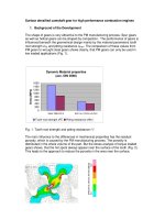
Low-temperature transparent conducting oxide (TCO) film is a prerequisite for
organic electronics that preclude the use of a high temperature process. For instance,
flexible organic light emitting devices (OLEDs) made with polyester, polyethylene
terephthalate (PET) and other plastic foils are not compatible with a high temperature
process. Therefore, the development of TCO films with smooth surfaces, high electric
conductivity and high optical transparency over the visible spectrum at a low processing
temperature is of practical importance for flexible OLEDs.
The aim of this research was to undertake a systematic study on the
development of high quality low-temperature indium tin oxide (ITO) films and the
optimization of its properties for device applications. A radio frequency (RF) magnetron
sputtering system was used for the film deposition. The electrical, optical, and surface
electronic properties were characterized and optimized. Different characterization
techniques including X-ray photoelectron spectroscopy (XPS), ultraviolet photoelectron
spectroscopy (UPS), in-situ four-point probe, atomic force microscopy (AFM), Hall
Effect, and UV-visible spectrophotometer were used.
The properties of the ITO films were optimized by introducing hydrogen species
into the sputtering gas mixture. ITO films with the thickness of 130 nm and sheet
resistance of 25 ± 5 Ω/sq can be fabricated over the hydrogen partial pressure from 1 –
3 × 10
-3
Pa and the films with an average transmittance of above 85% over the visible
VI
wavelength were obtained. The surface electronic properties of ITO films were found to
be relevant to the carrier concentrations. The work function can be modulated up to
~0.3 eV by varying the hydrogen partial pressures from 0 – 3.2 × 10
-3
Pa, which was
attributed to the variations in the surface band bending. The anode contact in an OLED
can be optimized by controlling ITO bulk carrier concentration and its surface
properties through surface modifications. These findings provided a basis for
engineering the ITO properties desired for an efficient OLED. Flexible OLEDs using
polymer-reinforced ultra-thin glass were fabricated. They had higher luminance than the
one made on the rigid glass because the polymer-reinforced ultra-thin glass has a better
refractive index match between the substrate and the OLED components, which may
enhance light extraction. A maximum efficiency of 5.1 cd/A at an operating voltage of 5
V was obtained. This was comparable to that of an identical device made with the
commercial ITO-coated rigid glass substrate. The surface electronic properties of NO-
treated ITO were also examined. A reduction in the carrier concentration near the
surface region of ITO, which was induced by NO adsorption, can result in a shift of
~0.2 eV in VBM edge. As a consequence, the presence of a NO-induced upward surface
band bending led to an increase in the sheet resistance. The clear understanding of the
interaction of ITO with NO enabled us to explore the potential of a room temperature
sensor using ITO as a sensing element in the QCM structure. The results confirmed the
effectiveness of NO modification of ITO surfaces and revealed that ITO has a potential
for NO sensors.
VII
LIST OF TABLES
Table 5.1 Average shrinkage of ultra-thin glass with a reinforcement
polymer layer.
Table 5.2 The results of bending test obtained for 50 micron-thick ultra-thin
glasses with a reinforcement polymer layer.
Table 6.1 The NO-induced low conductivity layer thickness and ΔR of the
ITO films exposed at different NO partial pressures.
Table 6.2 Comparison of atomic concentration of each element calculated
for different ITO surfaces.
VIII
LIST OF FIGURES
Fig. 2.1 The proposed band structure of undoped In
2
O
3
(a), and the effect
of Sn doping (b). (adapted from [2] I. Hamberg, C. G. Granqvist,
K. F. Berggren, B. E. Sernelius and L. Engstrom, Phys. Rev. B
30 (1984) 3240.)
Fig. 3.1 Multi-chamber vacuum system equipped with a magnetron
sputter, a plasma pre-treatment chamber, two device process
chambers and two glove boxes for device characterization &
testing.
Fig. 3.2 Schematic diagram of four-point probe technique.
Fig. 3.3 Sample geometries for performing Hall effect measurements.
Bar-shaped specimen (a), thin film sample used in the Van der
Pauw method (b) and clover-shaped sample (c). (Adapted from
[2] P. Y. Yu and M. Cardona, Fundamentals of Semiconductors:
Physics and Materials Properties (Berlin; New York: Springer,
c1996))
Fig. 3.4 A cross sectional view of OLED, where HTL is hole transporting
layer, the emitting layer can be small molecular or polymeric
electroluminescent materials.
Fig. 3.5 Ultra-thin flexible glass with reinforced polymer layer (a) and top
view of a patterned ITO for fabrication of OLEDs (b).
Fig. 3.6 Schematic diagram of an OLED fabrication procedure.
Fig. 3.7 Schematic flowchart of the ITO-QCM fabrication process.
Fig. 3.8 Schematic diagram of a gas sensor testing system for NO
detection.
Fig. 4.1 Sheet resistance and resistivity of ITO films as a function of
hydrogen partial pressure.
Fig. 4.2 Carrier concentration and Hall mobility of ITO films as a
function of hydrogen partial pressure.
Fig. 4.3 Transmittance of ITO films as a function of hydrogen partial
pressure.
IX
Fig. 4.4 UPS valence band spectra measured for ITO films prepared at
different hydrogen partial pressures of 0 Pa (a), 1.1 × 10
-3
Pa (b),
2 × 10
-3
Pa (c), 2.6 × 10
-3
Pa (d) and 3.2 × 10
-3
Pa (e),
respectively.
Fig. 4.5 Schematic energy band diagram showing surface band bending at
the ITO surface.
Fig. 4.6 Work function of ITO films as a function of carrier
concentration.
Fig. 4.7 J-V (a), L-V (b) and E-J (c) characteristic of OLEDs made on
ITO prepared at different hydrogen partial pressures of 2 × 10
-3
Pa (OLED1), 2.6 × 10
-3
Pa (OLED2) and 3.2 × 10
-3
Pa (OLED3),
respectively.
Fig. 4.8 He I UPS spectra obtained at ITO/NPB interface. The full spectra
are shown in the center part. The left and right graphs are
secondary electron cutoff and HOMO regions magnified for more
details. ITO films measured were deposited at different hydrogen
partial pressures of 0 Pa (a), 1.1 × 10
-3
Pa (b), 2 × 10
-3
Pa (c), 2.6
× 10
-3
Pa (d) and 3.2 × 10
-3
Pa (e).
Fig. 4.9 Schematic band diagram of electronic structure at ITO/NPB
interface. ITO films were prepared at different hydrogen partial
pressures of 2 × 10
-3
Pa (OLED1) (a), 2.6 × 10
-3
Pa (OLED2) (b)
and 3.2 × 10
-3
Pa (OLED3) (c), respectively.
Fig. 4.10 Interfacial barrier height at ITO/NPB as a function of carrier
concentration.
Fig. 4.11 Sn 3d
5/2
core level spectra obtained from untreated ITO film (a)
and NO plasma treated ITO (b).
Fig. 4.12 N 1s XPS spectra obtained from untreated ITO surface, NO-
adsorbed ITO surface and NO plasma treated ITO surface.
Fig. 4.13 J-V (a), L-V (b) and E-J (c) characteristics of OLEDs measured
for OLEDs made with untreated ITO (OLED1) and NO plasma
treated ITO (OLED2).
Fig. 5.1 Bending test of ultra-thin glass substrate using an Instron 5543
tester.
X
Fig. 5.2 Glass edges without (a) and with a layer of reinforcement
polymer layer (b).
Fig. 5.3 Schematic diagram showing the relationship between the
compression and vertical displacement of an ultra-thin glass
substrate along the compression direction.
Fig. 5.4 Schematic diagram of bending test for flexible substrate.
Fig. 5.5 Wavelength dependent transmittance of ITO-coated ultra-thin
glass with a reinforcement polymer layer.
Fig. 5.6 AFM image of an ITO film on the ultra-thin flexible glass.
Fig. 5.7 J-V (a), L-V (b) and E-V (c) characteristics of OLEDs measured
for OLEDs made with commercial ITO-coated rigid and
reinforced ultra-thin glass substrates. ITO1 and ITO2 were
prepared at hydrogen partial pressures of 1.1 × 10
-3
Pa and 2.6 ×
10
-3
Pa, respectively.
Fig. 6.1 Schematic diagram of a fresh ITO (a) and a dual layer ITO
consisting of a low conductivity layer, x, and bulk ITO layer, t
(b).
Fig. 6.2 N 1s core level spectra obtained from a clean ITO film (a), a NO-
adsorbed ITO surface (b) and a NO-adsorbed metal indium foil
(c).
Fig. 6.3 O 1s core level spectra measured from Ar
+
sputtered ITO surface
(a) and NO-adsorbed ITO surface (b).
Fig. 6.4 Sn 3d
5/2
core level spectra measured from a clean ITO surface (a)
and a NO adsorbed ITO surface (b).
Fig. 6.5 Valence band spectra obtained from a clean ITO film (dotted
line) and a NO-adsorbed ITO surface (solid line).
Fig. 6.6 Schematic energy diagram showing surface band bending of a
clean ITO (a) and a NO-adsorbed ITO (b).
Fig. 7.1 Time-dependent frequency shift of an ITO-QCM gas sensor (#2
ITO was prepared at a hydrogen partial pressure of 2 × 10
-3
Pa).
Fig. 7.2 Frequency sensitivity, S
f ,
as a function of NO concentration.
XI
Fig. 7.3 Repeatability of frequency shift of an ITO-QCM gas sensor (#2
ITO was prepared at a hydrogen partial pressure of 2 × 10
-3
Pa).
Fig. 7.4 Time-dependent frequency shifts of ITO-QCM gas sensors (#1
ITO and #3 ITO were prepared at hydrogen partial pressures of 0
and 2.6 × 10
-3
Pa, respectively).
Fig. 7.5 Frequency shifts of ITO-QCM gas sensors as a function of the
NO concentration (#1 ITO and #3 ITO were prepared at
hydrogen partial pressures of 0 and 2.6 × 10
-3
Pa, respectively).
Fig. 7.6 O 1s XPS spectra measured for ITO surface before and after NO
adsorption.
Fig. 7.7 N 1s XPS spectra measured for NO-adsorbed ITO surface before
and after the Ar
+
sputtering.
Fig. 7.8 Time-dependent changes of ITO sheet resistance.
XII
ABBREVIATIONS
AFM Atomic force microscopy
CBM Conduction band minimum
DC Direct current
EL Electroluminescence
E
c
Conduction band
E
f
Fermi energy level
E
opt
Optical band gap
E
v
Valence band
HOMO Highest occupied molecular orbital
HTL Hole transporting layer
ITO Indium tin oxide
J-V-L Current density-voltage-luminance
LUMO Lowest unoccupied molecular orbital
NO Nitric oxide
OLED Organic light-emitting device
PEDOT Poly(styrene sulfonate)-doped poly(3,4-ethylene dioxythiophene)
Ph-PPV phenyl-substituted poly(p-phenylenevinylene)
QCM Quartz crystal microbalance
RF Radio frequency
RMS Root mean square
R
s
Sheet resistance
XIII
TCO Transparent conducting oxide
T(λ) Wavelength dependent transmittance
UV Ultraviolet
UPS Ultraviolet photoelectron spectroscopy
Vs Surface potential
VBM Valence band maximum
XPS X-ray photoelectron spectroscopy
σ
Conductivity
N Carrier concentration
μ
Hall mobility
h
ν
Photon energy
ε Permittivity
XIV
LIST OF PUBLICATIONS
1. Jianqiao Hu, Furong Zhu, Jian Zhang and Hao Gong, A room temperature indium
tin oxide/quartz crystal microbalance gas sensor for nitric oxide, Sensors and
Actuators B, 93 (2003) 175.
2. J. Zhang, Jianqiao Hu, F. R. Zhu, H. Gong and S. J. O'Shea, ITO thin films coated
quartz crystal microbalance as gas sensor for NO detection, Sensors and Actuators
B, 87 (2002) 159.
3. Kaiyang Zeng, Furong Zhu, Jianqiao Hu, Lu Shen, Keran Zhang and Hao Gong,
Investigation of mechanical properties of transparent conducting oxide thin films,
Thin Solid Films, 443 (2003) 60.
4. Jianqiao Hu, Jisheng Pan, Furong Zhu and Hao Gong, Evidence of NO-induced
surface band bending of indium tin oxide observed by in situ four-point probe and
X-ray photoelectron spectroscopy, Journal of Applied Physics, 95 (2004) 6273.
5. Jianqiao Hu, Jisheng Pan, Furong Zhu, Hao Gong, Surface electronic structure of
nitric-oxide-treated indium tin oxide, Mat. Res. Soc. Symp. Proc. accepted.
6. Furong Zhu, Jianqiao Hu, Yoon Fei Liew, Kian Soo Ong and Xiaotao Hao, Effect
of surface electronic properties of ITO on luminance efficiency of OLED, Proc.
SPIE 5277 (2004) 163.
7. Kian Soo Ong, Jianqiao Hu, Roshan Shrestha, Furong Zhu and Soo Jin Chua,
Flexible polymer light-emitting devices using polymer-reinforced ultra-thin glass,
Thin Solid Films in press (2004). (highlighted in Technical Insights of Frost &
Sullivan)
XV
Chapter 1 Introduction
CHAPTER 1 INTRODUCTION
Thin films of transparent oxide semiconductors, also known as transparent
conducting oxides (TCOs), have widespread applications in opto-electronic devices due
to their unique properties of
high electric conductivity and optical transparency in the
visible wavelength region. Cadmium oxide (CdO) thin film, prepared by thermal
oxidation of sputtered-cadmium was the first material reported to possess both
transparent and conducting properties [1]. Although a thin layer of metal (~10-20 nm),
such as Au, Ag, Cu, etc., is electrically conducting and optically semitransparent, it is
usually not very stable as an active component in air for device applications. In
comparison with the semitransparent ultra-thin metal layer, thin films of TCOs have
advantages in many applications. This is because TCO layers are more stable, more
transparent and harder than metallic thin films in air.
In general, properly doped materials like ZnO, SnO
2
, and In
2
O
3
are used
individually or in separate layers or as mixtures such as indium tin oxide (ITO) and zinc
indium oxide (IZO) [2] for making TCO coatings. Almost all these TCO films are n-
type oxide semiconductors, in which the majority carriers are electrons induced by
stoichiometric deviation. There has been an increased research activity in development
of p-type TCOs. Kawazoe et al [3] reported that the transparent CuAlO
2
thin films have
p-type conductivity at room temperature. Although the conductivity of this new p-type
TCO was far lower than its n-type counterparts, it opened the way to some novel
1
Chapter 1 Introduction
applications using both n-type and p-type TCO layers to form a transparent p-n
junction.
The properties of TCO films are usually optimised accordingly to meet the
requirements in various applications that involve TCO materials. The light scattering
effect due to the usage of textured TCO substrates showed an enhanced absorbance in
thin film amorphous silicon solar cells [4,5]. However, a rough ITO surface is
detrimental for organic light emitting devices (OLEDs) applications. The high electric
fields created by the rough ITO anode can cause shorts in the thin functional organic
layers.
Among the existing TCOs, ITO is one of the most frequently used materials in
practical applications. Thin films of ITO have found many applications in anti-static
coatings, heat mirrors, solar cells [6], flat panel displays [7], sensors [8], and OLEDs [9-
11]. ITO film has attracted much attention because of its unique characteristics, such as
good conductivity, high optical transmittance over the visible wavelength region,
excellent adhesion to the substrates, stable chemical properties, and easy patterning
ability. These unique properties are very important for practical applications and are
strongly dependent on microstructure, stoichiometry, the nature of impurities in the
films and the deposition process.
The reproducible thin films of ITO can be prepared by many techniques
including thermal evaporation deposition [12], magnetron sputtering [13,14], electron
2
Chapter 1 Introduction
beam evaporation [15], spray pyrolysis [16], chemical vapour deposition [17], dip-
coating [18,19] and pulsed laser deposition methods [20,21]. Amongst these available
techniques for fabricating ITO films, the direct current (DC) or radio frequency (RF)
magnetron sputtering method is most often used to prepare ITO thin films for a wide
range of applications. The ITO film quality is determined by a number of factors such
as thickness uniformity, surface morphology, optical transparency and electrical
conductivity. In addition, the deposition technologies and the process conditions also
affect the structure and doping concentration.
ITO films have been widely used as transparent electrodes in flat panel
displays including plasma TVs, liquid crystal displays (LCDs) and OLEDs. The present
OLED technologies employ rigid substrates, such as glass, but flexible device structures
are extremely promising for future applications. The use of thin flexible substrates will
significantly reduce the weight of flat panel displays and provide the ability to bend a
display into any desired shape. Flexible OLEDs will also make possible the fabrication
of displays by continuous roll processing, thus providing the basis for very-low-cost
mass production. Because of this recent requirement in flexible OLEDs, there is a need
in depositing high quality ITO film on plastic or other flexible substrate. However,
plastic substrates, such as polyester, polyethylene terephthalate (PET) are not
compatible to high temperature plasma process, which is commonly used for depositing
ITO on the rigid glass [22]. Usually, a processing temperature of above 200
o
C is
required for preparing ITO films with the low electrical resistivity and high optical
transparency in the visible wavelength region [23]. ITO films formed at a processing
3
Chapter 1 Introduction
temperature below 200
o
C often have relatively higher resistivity and lower optical
transparency than the films prepared at a high substrate temperature. In the application
of organic electronics, it is often required to coat an active layer on functional organic
substrates that are not compatible with a high processing temperature. Therefore the
development of high quality ITO films with smooth surfaces, low resistivity and high
transmission over the visible spectrum at a low processing temperature is of practical
importance.
In addition to the unique optical and electrical characteristics of bulk ITO, the
surface properties of ITO also play an important role in determining the device
performance. For example, ITO is used as one of the active components in gas sensors.
The sensitivity of ITO sensors is related closely to the changes in the film resistance
that is induced due to the modification of the surface potential. Therefore, the
fundamental understanding of interaction between ITO and target gases is important.
The ITO contact in OLED plays a crucial role in determining the device performance.
At the moment the availability of ITO in the market is mainly for the use in the
fabrication of LCD, which may not be ideal for the OLED application. In OLEDs, ITO
serves anode for the hole injection. Interface between ITO and organic material has
attracted considerable interest. Much effort has been focused on understanding the
effect of ITO surface electronic properties on OLED performance. Different ITO
surface modifications including various surface cleaning techniques using acid or base
solutions [24], and a variety of plasma treatments [25-28] have been reported.
4
Chapter 1 Introduction
The purpose of this work was to carry out a systematic research on developing
high quality ITO films at a low processing temperature, studying their optical, electrical
and surface electronic properties and exploring their potential for device applications. It
aims at obtaining high performance ITO thin film with desired properties at a low
processing temperature for OLED and sensor applications. The principal objectives of
the work are:
1. to develop high performance ITO using RF magnetron sputtering at a low
temperature and optimize the process conditions for potential device
fabrications;
2. to characterize and analyze the electrical, optical and surface electronic
properties of ITO films;
3. to study the effect of surface electronic properties of ITO on luminance
efficiency of OLED;
4. to investigate nitric oxide (NO) adsorption on ITO surface and explore the use
of ITO in QCM for sensor application.
The results obtained from this work provided a technical guidance and
fundamental understanding for developing high quality ITO films that are suitable for
use in organic electronics. Both material properties and processing conditions were
investigated and optimized. The low temperature ITO thus developed was also used as
anode for OLEDs. A set of identical OLEDs was made on ITO with different carrier
concentrations. The current density-luminance-voltage characteristics (J-L-V) of the
devices indicated that the carrier concentration in ITO played a role in improving the
5
Chapter 1 Introduction
device performance. The increase in luminance efficiency of the OLEDs reflected an
improved hole-electron current balance in the device. The origin of the ITO band
bending and its effect on hole-injection in an OLED were discussed. Electroluminescent
(EL) performance of OLED made with NO plasma treated ITO was also improved
substantially. The results obtained have direct implications for developing novel
OLEDs using flexible plastic substrates. In addition, a clear understanding on the
interaction of ITO with NO also provided a basis for exploring potential applications of
ITO-coated quartz crystal microbalance (QCM) gas sensors.
The following chapter provides a brief summary of basic properties and the
results of some recent topical research work on TCO. The material properties and
technical aspects related to the ITO films, including the principles of sputtering
technique, ITO band structure, conduction mechanism and the optical properties of ITO
films are discussed.
6
Chapter 1 Introduction
References:
1. H. L. Hartnagel, A. L. Dawar, A. K. Jain and C. Jagadish, Semiconducting
Transparent Thin Films (Institute of Physics Publishing, Bristol, 1995).
2. J. Nishino, T. Kawarada, S. Ohshio, H. Saitoh, K. Maruyama and K. Kamata, J.
Mater. Sci. Lett. 16 (1997) 629.
3. H. Kawazoe, M. Yasukawa, H. Hyodo, M. Kurita, H. Yanagi and H. Hosono,
Nature 389 (1997) 939.
4. B. Schröder, Mater. Sci. Eng. A 139 (1991) 319.
5. F. Zhu, T. Fuyuki, H. Matsunami and J. Singh, Sol. Energ. Mat. Sol. C 39
(1995) 1.
6. K. L. Chropra, S. Major and D. K. Pandya, Thin Solid Films 102 (1983) 1.
7. B. H. Lee, I. G. Kim, S. W. Cho and S. H. Lee, Thin Solid Films 302 (1997) 25.
8. B. J. Luff, J. S. Wilkinson and G. Perrone, Appl. Optics 36 (1997) 7066.
9. J. S. Kim, M. Granström, R. H. Friend, N. Johansson, W. R. Salaneck, R. Daik,
W. J. Feast and F. Cacialli, J. Appl. Phys. 84 (1998) 6859.
10. I. D. Parker, J. Appl. Phys. 75 (1994) 1656.
11. C. C. Wu, C. I. Wu, J. C. Sturm and A. Kahn, Appl. Phys. Lett. 70 (1997) 1348.
12. A. Salehi, Thin Solid Films 324 (1998) 214.
13. K. Zhang, F. Zhu, C. H. A. Huan and A. T. S. Wee, J. Appl. Phys. 86 (1999)
974.
14. K. Zhang, F. Zhu, C. H. A. Huan, A. T. S. Wee and T. Osipowicz, Surf.
Interface Anal. 28 (1999) 271.
7
Chapter 1 Introduction
15. J. K. Sheu, Y. K. Su, G. C. Chi, M. J. Jou and C. M. Chang, Appl. Phys. Lett.
72 (1999) 3317.
16. S. Major and K. L. Chopra, Sol. Energy Mater. 17 (1988) 319.
17. J. Hu and R. G. Gordon, J. Appl. Phys. 72 (1992) 5381.
18. Y. Takahashi, S. Okada, R. B. H. Tahar, K. Nakano, T. Ban and Y. Ohya, J.
Non-Crystalline Solids 218 (1997) 129.
19. K. Nishio, T. Sei and T. Tsuchiya, J. Materials Sci. 31 (1996) 1761.
20. H. S. Kwok, X. W. Sun and D. H. Kim, Thin Solid Films 335 (1998) 299.
21. H. Kim, A. Piqué, J. S. Horwitz, H. Mattoussi, H. Murata, Z. H. Kafafi and D.
B. Chrisey, Appl. Phys. Lett. 74 (1999) 3444.
22. P. F. Carcia, R. S. Mclean, M. H. Reilly, Z. G. Li, L. J. Pillione and R. F.
Messier, J. Vac. Sci. Technol. A 21(3) (2003) 745.
23. D. Y. Lee, S. J. Lee, K. M. Song and H. K. Baik, J. Vac. Sci. Technol. A 21(4)
(2003) 1069.
24. F. Nuesch, L. J. Rothberg, E. W. Forsythe, Q. T. Lee and Y. L. Gao, Appl. Phys.
Lett. 74 (1999) 880.
25. C. C. Wu, C. I. Wu, J. C. Sturm and A. Kahn, Appl. Phys. Lett. 70 (1997) 1348.
26. D. J. Milliron, I. G. Hill, C. Shen, A. Kahn and J. Schwartz, J. Appl. Phys. 87
(2000) 572.
27. B. Choi, H. Yoon and H. H. Lee, Appl. Phys. Lett. 76 (2000) 412.
28. B. L. Low, F. R. Zhu, K. R. Zhang and S. J. Chua, Appl. Phys. Lett. 80 (2002)
4659.
8
Chapter 2 Theory and literature review
CHATPER 2 THEORY AND LITERATURE REVIEW
2.1 Band structure of ITO
ITO is formed by substitutional doping of In
2
O
3
with Sn which replaces the In
3+
atoms from the cubic bixbyte structure of indium oxide [1]. Sn in ITO is postulated to
form an interstitial bond with oxygen and it exists either as SnO or SnO
2
with the
valence of +2 and +4 respectively. Sn
2+
results in a net reduction in carrier
concentration as a hole is created, acting as a trap and reducing conductivity. Sn
4+
substitutes for the In
3+
cation creating a donor level in the energy band gap and
releasing electrons to the conduction band as an n-type donor. On the other hand, In
2
O
3
is usually oxygen deficient. The oxygen vacancies give rise to a shallow donor level just
below the conduction band. They act as doubly ionized donors and contribute at
maximum two electrons. Therefore, both substitutional tin dopants and oxygen vacancy
donors contribute to the conductivity of ITO.
Hamberg and Granqvist [2] have proposed a simple band structure to explain the
conduction mechanism in In
2
O
3
. According to their model, both doped-In
2
O
3
and un-
doped In
2
O
3
band structures, shown in Fig. 2.1 are parabolic. With the top of the
valence band as reference energy, the dispersions for the unperturbed valence band,
E
v
0
(k), and conduction band, E
c
0
(k), can be expressed as:
E
v
0
(k) = − ћk
2
/2m
v
*
,
(2.1)
and
9