MULTI PHOTON ABSORPTION INDUCED PHOTOLUMINESCENCE IN DOPED SEMICONDUCTOR QUANTUM DOTS AND HETERO NANOSTRUCTURES
Bạn đang xem bản rút gọn của tài liệu. Xem và tải ngay bản đầy đủ của tài liệu tại đây (6.38 MB, 173 trang )
MULTI-PHOTON ABSORPTION INDUCED
PHOTOLUMINESCENCE IN
DOPED SEMICONDUCTOR QUANTUM DOTS
AND HETERO-NANOSTRUCTURES
A THESIS
submitted by
Radhu. S
for the award of the degree
of
JOINT DOCTOR OF PHILOSOPHY
DEPARTMENT OF PHYSICS
INDIAN INSTITUTE OF TECHNOLOGY MADRAS
AND NATIONAL UNIVERSITY OF SINGAPORE
MAY 2015
DECLARATION
I hereby declare that all the experiments embodied in this thesis entitled, “MULTI-PHOTON
ABSORPTION INDUCED PHOTOLUMINESCENCE IN DOPED SEMICONDUCTOR
QUANTUM DOTS AND HETERO-NANOSTRUCTURES”, submitted for the degree of
Joint Doctor of Philosophy in Physical Sciences to Indian Institute of Technology Madras and
National University of Singapore, under the Indo-NUS Joint PhD program, has been carried out
by me at Department of Physics, IIT Madras, India and Department of Physics, National
University of Singapore, Singapore under the supervision of Prof. C. Vijayan and Prof. Wei Ji.
The contents of this thesis, in full or part, have not been submitted to any other Institute or
University for the award of any degree or diploma.
Date: 19 May, 2015 RADHU. S
Department of Physics
Indian Institute of Technology Madras
Chennai – 600036
CERTIFICATE
This is to certify that the work incorporated in the thesis entitled, “MULTI-PHOTON
ABSORPTION INDUCED PHOTOLUMINESCENCE IN DOPED SEMICONDUCTOR
QUANTUM DOTS AND HETERO-NANOSTRUCTURES” submitted by Ms. RADHU. S,
has been carried out by her under our supervision at Department of Physics, Indian Institute of
Technology Madras, Chennai, 600 036, India and Department of Physics, National University of
Singapore, Singapore, 119077. The contents of this thesis, in full or part, have not been
submitted to any other Institute or University for the award of any degree or diploma.
Prof. C. Vijayan Prof. Wei Ji
(Research Guide) (Research Guide)
Photonics Laboratory Department of Physics
Department of Physics Faculty of Science
Indian Institute of Technology Madras National University of Singapore
Chennai -600036 2 Science Drive 3, Singapore-117542
Tel: 91-44-2257 4877 Tel: (65)65166373
Email: Email:
Date: 19-05-2015
Place: Chennai
Dedicated to…
My Husband, Sasidevan. V
&
My Parents, P.K. Radhakrishna Panicker and S. Subhakumari
&
My Brother, Sambhu. R
i
ACKNOWLEDGEMENT
I would like to thank all the people and Institutions who helped and supported me for the
completion of my PhD work as well as to finish this dissertation. First and foremost, I would like
to thank my supervisors, Prof. C. Vijayan (IITM) and Prof. Wei Ji (NUS) for their constant
encouragement, motivation and guidance. I have faced many difficulties in my personal life
during this PhD and I would like to express my sincere gratitude to Prof. C. Vijayan who cared
me and supported me during these times, just like my father. Also, his sincere efforts made it
possible for me to work in National University of Singapore under the Joint PhD program. It is a
great privilege for me to work with Prof. Ji Wei in NUS. I would like to express my deepest
gratitude to Prof. Ji Wei for his inspiring and motivating attitude and willingness to come for
discussions, even on holidays, which helped me a lot to improve myself. I would also like to
thank him for doing all the necessary arrangements to extend my candidature period in NUS and
arranging financial support during this period, which helped me to complete this work.
I would like to thank IITM and NUS authorities, especially Prof. Markandeylu (former HOD,
Dept. Of Physics, IITM), Prof. Sunil Kumar (HOD, Dept. of Physics, IITM) and Prof. B.V.R.
Chowdhary (Dept. of Physics, NUS) for giving me a wonderful opportunity to work in both the
prestigious Institutes. I would like to express my gratitude to my Doctoral Committee members,
Prof. M. P. Kothiyal, Prof. Kasi Viswanathan, and Prof. Nilesh. J. Vasa and Prof. Edamana
Prasad for their suggestions and comments in my work. I would also like to thank Prof. Lakshmi
Bala and Prof. Rajesh Narayanan for their encouragement and support. The financial assistance
from University Grants Commission, during my stay in IITM is also duly acknowledged. I would
also like to express my gratitude to Prof. K.R. Somanatha Pillai, D. B. Pampa College, Parumala
for his constant care, encouragement and discussions. I would like to thank Prof. Taeghwan
Hyeon (Seoul National University, South Korea) and Prof. Wee Shong Chin (Dept. of
Chemistry, NUS) for providing quantum dot and nanorod samples.
My lab members in IITM and NUS have been a big support for me. I would like to express
my heart-felt gratitude to Dr. Venkatram Nalla for his invaluable help in Femtosecond
laboratory, NUS, as well as for all the discussions during the different stages of my work which
helped me to finish this dissertation. I am glad to thank my labmates in IITM and NUS, Dr.
ii
Manas, Dr. Jyotsana, Dr. Anitha, Mr. Jayachandra, Ms. Radhika, Mr. Shiva, Mr. Xu Zhe, Mr.
Venkatesh Mamidala and Mr. Chen Weiquiang for their support and encouragement. I would
like to remember with thanks the time I spent with Dr. Aparna Devi, Dr. Christie Thomas
Cherian, Dr. Sinu Thomas and their families. I have immense pleasure in thanking my friends in
IITM and NUS, Ms. Saritha, Dr. Safina Devi, Dr. Shani Jose, Dr. Pramitha. V, Ms. Lizbeth Zeta,
Dr. Anjana C.P, Dr. Suruchi, Ms. Kavitha K.G., Dr. Lekha P.K, Ms. Rusha, Dr. Robin John, Ms.
Kavitha, Ms. Deepthy, ms. Divya and Ms. Ganga who made my stay pleasant and memorable. I
am expressing my deepest gratitude to Ms. Lincy for her love, care and support, which helped
me a lot during thesis submission.
I would never have been able to finish this work without the invaluable support from my
family. My father, Radhakrishna Panicker (Late), have been my inspiration to pursue research in
Science. Words can’t express my gratitude to him for the love and care he gave me. I remember
with love at this moment, his decision to allow me to continue my studies even when he was
struggling for life. My mother, Subhakumari, has been my biggest support all these times. It is
her love, courage, support and prayers which helped me to move forward in life and reach this
stage in both academic and personal life. I am lucky to have a wonderful brother, Sambhu, who
was there for me every time I needed a help, being it personal or academic. My husband,
Sasidevan came to my life just after the first year of my PhD. From that time onwards, he has
been with me as my best friend and soulmate. It is just because of his invaluable support that I
was able to go to Singapore and the decision was taken at a time, when he needed my help the
most. I recall at this moment, all the love and encouragement he has given me to finish this
work. I express my deepest gratitude to my grandparents, Kunjunnithan, Devakiamma and
Saradaamma, and my sister-in-law, Nandinikutty, for their support to continue my studies.
Finally, I would like to thank all other family members especially, my uncles and aunts, my
cousins, my mother-in-law Leela.P, Jayakrishnan, Harikrishnan and Unnikrishnan for their love
and care. Last, but not the least, I would like to thank God almighty for all his blessings to
complete this work.
iii
ABSTRACT
Materials with high multi-photon absorption cross-section are of recent interest in opto-
electronic and biological applications such as lasing, optical limiting, three-dimensional data
storage, multi-photon microscopy etc. Owing to the properties such as remarkable photo
stability, brightness and size dependent absorption and emission, semiconductor nanocrystals
(NCs) are preferred over other conventional fluorophores as bio-imaging probes in multi-photon
microscopy. The major impediment to use multi-photon absorption in NCs for practical
applications is the requirement of high excitation intensity because of the low absorption cross-
section of nanocrystals in near-infrared (NIR) wavelengths. This dissertation aims at enhancing
the multi-photon absorption cross-section of nanocrystals in NIR wavelengths by doping and by
forming hetero-nanostructures. Specifically, this thesis presents the nonlinear optical
investigations of the multi-photon absorption induced photoluminescence in Mn
2+
-doped ZnS
nanocrystals and CdS-CdSe-CdS segmented nanorods. In addition to the nonlinear absorption
studies, the charge transfer dynamics in CdS-CdSe-CdS segmented nanorods is also presented in
this thesis.
An introduction to the optical properties of semiconductor NCs is given in the beginning
of Chapter 1 followed by a brief introduction to hetero-junction nanomaterials. The succeeding
section deals with the carrier dynamics in single component and hetero-junction semiconductor
NCs. In the subsequent section the basics of multi-photon absorption (MPA) and related optical
nonlinearities, which lay the foundation for the work presented in this thesis, are outlined. This is
followed by a review on the MPA studies in single component and hetero-junction
semiconductor NCs. This is followed by a discussion on the significance of excitation in NIR-I
and NIR-II window. The objectives and scope of the work presented in this thesis are outlined in
the concluding section of Chapter 1. The operational principles of the different techniques used
for the non-linear optical characterization and carrier dynamics study such as Z-scan technique,
transient pump-probe spectroscopy, and multi-photon absorption induced photoluminescence
(MPA-PL) measurements are discussed in Chapter 2.
Doping can modify the photoluminescence (PL) emission wavelength of semiconductor
NCs by introducing additional levels in the energy gap. ZnS is a less cytotoxic material with less
PL quantum yield. The emission wavelength in these NCs can be shifted to NIR wavelengths, by
iv
finding appropriate dopants. In Chapter 3, we present our results on the red emission in ZnS NCs
where we propose that the emission in ZnS nanocrystals can be shifted to NIR-I window by
doping with O
2-
ions, in the presence of interstitial sulfur ions in these NCs. Besides changing
the excitation and emission, the quantum confinement effect in QDs as well as the strain in the
lattice due to defects can change other properties as well, such as shift in the vibrational modes
of the lattice. Raman spectroscopic studies in these O
2-
doped ZnS NCs were also presented in
chapter 3 which gives a better understanding on the shift in the vibrational modes on reducing
the size of semiconductor from bulk to nanometer range.
Transition metal doping can change the multi-photon absorption cross-section in
semiconductor NCs besides changing the emission wavelength and PL quantum yield. Chapter 4
primarily deals with understanding the effect of Mn
2+
-doping in the MPA properties of ZnS QDs
on excitation in NIR-I and NIR-II window. In the first section of Chapter 4, we present the
derivation of 3PA theory for wide band gap semiconductor QDs (direct band gap) such as ZnS,
without considering the presence of any defect levels in the band gap. The details of the
synthesis procedure and linear optical characterization studies in Mn
2+
-doped ZnS QDs are
presented in the subsequent sections. This section is followed by our investigation on the multi-
photon action cross-section of Mn
2+
-doped ZnS QDs on excitation in NIR-I window. With the
intention of understanding the effect of Mn
2+
doping on determining the multi-photon action
cross-section in doped ZnS QDs, the results are compared with undoped ZnS QDs of similar size
as well as the theoretical prediction under four band model for undoped ZnS QDs of similar size,
without defects. The succeeding section of Chapter 4 describes our investigation of multi-photon
action cross-section on excitation in NIR-II window. The chapter is concluded with the transient
PL measurements in Mn
2+
-doped ZnS QDs on multi-photon excitation.
Apart from changing the size of the NC or doping, a different method to enhance two-
photon absorption over a wide range of wavelength is to form composites where the constituent
components already possess large two-photon absorption. Here, local field can determine the
effective two-photon absorption cross-section, in addition to the weighted averages of the
component semiconductors and hence providing a way to engineer the optical nonlinearity in
semiconductor NCs. Chapter 5 deals with this aspect, in particular, the chapter focuses on the
investigation of multi-photon absorption properties in CdS-CdSe-CdS segmented nanorods. The
v
procedure for the synthesis of CdS-CdSe-CdS segmented nanorods is presented in the first
section of this chapter. This is followed by the analysis of the linear optical characterization in
these nanorods. The next section deals with the Z-scan measurements as well as the multi-photon
absorption induced PL measurements in CdS-CdSe-CdS nanorods. The effect of the composite
structure on the optical non-linear properties of CdS-CdSe-CdS segmented nanorods is also
examined in this chapter by considering the effect of local field, as suggested by Maxwell-
Garnett theory.
The superior photoluminescence of CdS-CdSe hetero-nanostructures is a result of the
efficient charge transfer from CdS to CdSe and subsequent recombination in CdSe. In the final
chapter (Chapter 6), we investigate the dynamical properties of photo excited carriers in CdS-
CdSe-CdS segmented nanorods using femtosecond transient pump-probe spectroscopy. The
carriers generated in CdS can have different relaxation channels with charge transfer to CdSe
being a dominant mechanism. Different relaxation mechanisms of the photo generated carriers in
CdS segments have been investigated in this chapter. Excitation at higher intensities is required
for applications such as multi-photon microscopy. As the intensity increases, other relaxation
mechanisms such as Auger recombination can become significant in semiconductor NCs and
these mechanisms can considerably affect the charge transfer also, resulting in reduced PL
quantum yield at high intensities. In Chapter 6, we also present our investigations on the charge
transfer dynamics in CdS-CdSe-CdS segmented nanorods at high excitation intensities (when the
average number of electron-hole pair per nanorod greater than unity). In particular, we examined
the effect of Auger recombination on charge transfer in CdS-CdSe-CdS segmented nanorods.
The present work is expected to lead to a better understanding of the non-linear optical
properties of nanomaterials and provide a platform for engineering their non-linear absorption,
thereby making it suitable for applications in bio-imaging and photonics.
vi
TABLE OF CONTENTS
ACKNOWLEDGEMENT……………………………………………………………………….i
ABSTRACT…………………………………………………………………………………… iii
LIST OF FIGURES…………………………………………………………………………….ix
LIST OF TABLES…………………………………………………………………………… xiii
LIST OF PUBLICATIONS………………………………………………………………… xiv
ABBREVIATIONS…………………………………………………………………………… xv
Chapter 1. Introduction…………………………………………………………………………1
1.1. Background…………………………………………………………………… …1
1.2. Previous Research on Quantum Dots, Nanorods and Hetero-junction
nanocomposites……………………………………………………………… … 3
1.2.1. Quantum Dots and Nanorods………………………………………… 3
1.2.2. Hetero-junction nanomaterials……………………………………… 10
1.2.3. Carrier dynamics in nanomaterials…………………………………… 12
1.2.4. Multi-photon absorption and related optical nonlinearities in
semiconductor NCs………………………………………………… ….14
1.2.4.1. Nonlinear absorption………………………………………… 15
1.2.4.2. Nonlinear refraction………………………………………… 19
1.2.4.3. Nonlinear scattering…………………………………………… 19
1.2.4.4. Previous research on MPA in semiconductor NCs………… 20
1.2.5. Significance of NIR-I and NIR-II windows…………………………… 23
1.3. Objectives and Scope of the thesis………………………………………… … 26
Chapter 2. Experimental methods and techniques………………………………….……… 27
2.1. Z-scan technique……………………………………………………… …………27
vii
2.1.1. Z-scan theory……………………………………………………… … 28
2.2. Transient pump-probe spectroscopy…………………………………………… 36
2.3. Multi-photon absorption induced PL technique………………………………… 38
Chapter 3. Defect induced photoluminescence and confined phonon modes in ZnS
nanoparticles………………………………………………………………………41
3.1. Introduction……………………………………………………………… ………41
3.2.Materials and methods……………………………………………… ………… 42
3.3.Results and discussion…………………………………………………… ………43
3.3.1. Optical absorption studies……………………………………………43
3.3.2. Structural analysis and morphological studies……………………….44
3.3.3. Photoluminescence studies……………………………………… 45
3.3.4. Elemental analysis using EDAX and X-ray photoelectron
spectroscopy……………………………………………………….…46
3.3.5. Proposed mechanism for the observed emission bands………….… 49
3.3.6. Raman spectroscopic studies……………………………………… 56
3.4. Conclusion……………………………………………………………………… 59
Chapter 4. Multi-photon absorption induced photoluminescence in Mn
2+
-doped ZnS
quantum dots ………………………………………………………………………61
4.1. Introduction……………………………………………… ……………………62
4.2. Theory for 3PA in ZnS QDs……………………………………………… …….64
4.3. Materials and methods……………………………………………………… … 68
4.3.1. Synthesis of Mn
2+
-doped ZnS QDs……………………………… 68
4.3.2. Linear optical characterization……………………………………….69
4.3.3. Multi-photon absorption induced photoluminescence in Mn
2+
-doped
ZnS QDs on excitation in near-infrared window I…….…………… 72
4.3.4. Multi-photon absorption induced photoluminescence in Mn
2+
-doped
ZnS QDs on excitation in near-infrared window II…… 80
viii
4.3.5. Transient PL measurements………………………………………….87
4.4. Conclusion………………………………………………………………….…… 89
Chapter 5. Two-photon absorption induced photoluminescence in CdS-CdSe-CdS
segmented nanorods ……………………………………………………… ……91
5.1. Introduction………………………………………………………… ………… 91
5.2. Materials and methods…………………………………………………… …… 95
5.3. Results and discussions……………………………………………………… ….96
5.3.1. Structural analysis………………………………………………… 96
5.3.2. Linear optical characterization……………………………………….99
5.3.3. Two-photon absorption and two-photon excited PL……………….104
5.3.3.1. Z-scan technique……………………………………………… 104
5.3.3.2. Multi-photon absorption induced PL studies………………… 107
5.4. Conclusion……………………………………………………………………….110
Chapter 6. Carrier dynamics in CdS-CdSe-CdS segmented nanorods ………………….112
6.1. Introduction…………………………………………….…………… … 112
6.2. Carrier dynamics in nanomaterials…………………………….…………115
6.3. Experimental details………………………………………………… ….118
6.4. Results and discussions………………………………………………… 119
6.5. Conclusion…………………………………………………………….….131
Chapter 7. Summary and future outlook ……………………………………………….….133
7.1. Summary and conclusion…………………………………………………133
7.2. Suggestions for future work………………………………………………135
References…………………………………………………………………………………… 137
ix
LIST OF FIGURES
Figure 1.1. Electronic energy states of a semiconductor in the transition from discrete molecules
to Quantum Dots (QDs) and bulk crystals………………………………………… 6
Figure 1.2. Evolution of the “density of states” function from a bulk material (3D solid) to a
2D,1D and 0D system……………………………………………………………….8
Figure 1.3. Schematic diagram showing two-photon absorption and three-photon absorption in a
two-level system………………………………………………………………… 16
Figure 1.4. Schematic diagram showing excited state absorption………………………………17
Figure 2.1. Schematic diagram showing the experimental setup for OA Z-scan technique…….32
Figure 2.2. Schematic diagram showing the experimental setup for CA Z-scan technique…….33
Figure2.3. Schematic diagram showing the experimental setup for transient pump-probe
spectroscopy……………………………………………………………………… 38
Figure 2.4. Schematic diagram showing the experimental setup for MPA-PL measurement… 39
Figure 3.1. Optical absorption spectrum of ZnS nanoparticles synthesized at 150
0
C………….44
Figure 3.2. X- Ray powder diffraction pattern of ZnS nanoparticles synthesized at 150
0
C… 45
Figure 3.3. TEM image, showing nanoparticles in the size range of 3 – 12 nm……………… 47
Figure 3.4. HRTEM image showing the lattice fringes of ZnS nanoparticles………………… 47
Figure 3.5. Photoluminescence spectra of ZnS nanoparticles synthesized at 150
0
C………… 48
Figure 3.6. EDAX pattern, showing the presence of oxygen in the sample along with zinc and
sulphur…………………………………………………………………………… 50
Figure 3.7. XPS spectrum of the sample synthesized at 150
0
C……………………………… 51
Figure 3.8. Energy level diagram explaining the observed emission bands…………………….52
x
Figure 3.9. Optical absorption spectrum for the samples synthesized at 170
0
C…………….….53
Figure 3.10.Comparison of photoluminescence spectra of ZnS nanocrystal samples synthesized
at 170
0
C and at 150
0
C.……………………………………………………………54
Figure 3.11. Photoluminescence in the samples synthesized at 170
0
C…………………………55
Figure 3.12. Shift in the PL emission band in the samples synthesized at 170
0
C before and after
annealing at 400
0
C for 30 minutes……………………………………………… 56
Figure 3.13. Raman Spectrum of ZnS nanoparticles synthesized at 150
0
C…………………….57
Figure 4.1. Three possibilities of 3PA transitions from valence band to conduction band… 67
Figure4.2(a).Transmission Electron Microscopic (TEM) images of Mn
2+
-doped ZnS QDs
showing an average size of 5.5 nm……………………………………………… 70
Figure4.2(b). UV-Visible absorption spectrum for Mn
2+
-doped ZnS QDs fitted with Gaussian
curves………………………………………………………………………………70
Figure4.2(c). One-photon PLE and PL spectra of Mn
2+
-doped ZnS QDs………………………71
Figure 4.3. Energy level diagram explaining the one-photon- absorption-induced photodynamics
in Mn
2+
-doped ZnS QDs and undoped ZnS QDs…………………………………72
Figure 4.4.(a) Multi-photon-excited PL emission spectra of Mn
2+
-doped ZnS QDs, undoped ZnS QDs
and Rhodamine 6G………………………………………………………………………74
Figure 4.4.(b) Multi-photon-excited PL emission spectra of Mn
2+
-doped ZnS QDs and undoped
ZnS QDs on excitation at 950 nm………………………………………………….75
Figure 4.5. Excitation fluence dependence of multiphoton excited PL peak intensity for Mn
2+
-
doped ZnS QDs at different excitation wavelengths…………………………… 76
Figure 4.6. Energy level diagram explaining the multi-photon-absorption-induced
photodynamics in Mn
2+
-doped ZnS QDs and undoped ZnS QDs…………………77
xi
Figure 4.7. Comparison of the three-photon action cross-section estimated for Mn
2+
-doped ZnS
QDs and undoped ZnS QDs with the theoretical four band model… 79
Figure 4.8. Multi-photon-excited PL emission spectra of Mn
2+
-doped ZnS QDs and Rhodamine 6G on
excitation at 1060 nm…………………………………………………………………….81
Figure 4.9. Excitation fluence dependence of multi-photon excited PL peak intensity for Mn
2+
-doped ZnS
QDs at different excitation wavelengths……………………………………………… 82
Figure 4.10. Slope obtained from the log-log plot of PL peak intensity (586 nm) with excitation fluence
for Mn
2+
-doped ZnS QDs at different excitation wavelengths…………………………83
Figure 4.11. Energy level diagram explaining the one-photon- and multi-photon-absorption-induced
photodynamics in Mn
2+
-doped ZnS QDs……………………………………………….84
Figure 4.12. Two-photon action cross-section estimated for Mn
2+
-doped ZnS QDs in the range
from 1050 nm to 1300 nm…………………………………………………………85
Figure 4.13. Comparison of two-photon action cross-section in Mn
2+
-doped ZnS QDs in NIR-II
(g) with other chromophores such as organic dye molecules and fluorescent
proteins…………………………………………………………………………… 86
Figure 4.14. (a) Multi-photon-excited PL lifetime measurements in Mn
2+
-doped ZnS QDs
(emission at 586 nm) at different excitation wavelengths……………………….88
Figure 5.1. Band alignment in different kinds of hetero-nanostructures………………………94
Figure 5.2. (a) Schematic structure of the CdS-CdSe-CdS segmented nanorods …………….97
Figure 5.2.(b) HRTEM images of the CdS-CdSe-CdS segmented nanorods for Sample 1-1-
1…………………………………………………………………………………….97
Figure 5.2.(c) HRTEM images of the CdS-CdSe-CdS segmented nanorods for Sample 2-1-
2…………………………………………………………………………………….97
Figure 5.2.(d) SAED pattern of the CdS-CdSe-CdS segmented nanorods……………………97
Figure 5.2.(e) The structure of segmented nanorods were determined by identifying the d-spacing
at three different regions of the nanorod…………………………………………………………98
Figure 5.3.(a) The band alignment diagram of CdS and CdSe showing the valence band and
conduction band offset…………………………………………………………….99
xii
Figure 5.3.(b) Schematic diagram showing electronic delocalization in the conduction band of
CdS-CdSe-CdS segmented nanorods and the localization of holes in CdSe
segments……………………………………………………………………………99
Figure 5.4. Optical properties of CdS-CdSe-CdS segmented nanorods……………………….101
Figure 5.5. The relative measurement of quantum yield will give idea about the charge transfer
from CdS to CdSe……………………………………………………………… 103
Figure 5.6. Open-Aperture Z- Scan curves obtained from CdS-CdSe-CdS segmented nanorods at
800 nm for different excitation irradiances………………………………………105
Figure 5.7. Two-photon action cross-section estimated for CdS-CdSe-CdS segmented nanorods
in the range of incident photon energy 0.95 eV to 1.55 eV…………………….109
Figure6.1. Schematic representation of two types of Auger effects in semiconductor
nanocrystals……………………………………………………………………….117
Figure 6.2. Transient differential transmission signal from CdS-CdSe-CdS segmented nanorods
with pump at 2.5 eV………………………………………………………………120
Figure 6.3. Transient differential transmission signal from CdS-CdSe-CdS segmented nanorods
with pump and probe at 2.5 eV in a 2 ns window……………………………….123
Figure 6.4. Quantized steps in quantum-confined Auger recombination in QDs……………125
Figure 6.5. Intensity dependent decay observed in Sample 2-1-2 and Sample 1-1-1 with pump
and probe at 2.5 eV……………………………………………………………….126
Figure 6.6. Transient differential transmission signal from CdS-CdSe-CdS segmented nanorods
with pump at 2.5 eV corresponding to the excitonic state of CdS and with the probe
signal at 1.98/2.02 eV (Sample 2-1-2/Sample 1-1-1)…………………………….128
Figure 6.7.(a) Charge transfer time τ extracted from the exponential fit in Figure 6.6 is plotted
with varying <N> for CdS-CdSe-CdS segmented nanorods…………………….128
Figure 6.7.(b) A change in the decay (with pump and probe at 2.5 eV) is observable in the initial
time scale of ~ 1 picoseconds after photo-excitation at large <N> when Auger
recombination is present………………………………………………………….129
Figure 6.8. Schematic diagrams illustrating the charge transfer in CdS-CdSe-CdS segmented
nanorods in the absence (<N> << 1) and presence (<N> >>1) of Auger
Recombination……………………………………………………………………130
xiii
LIST OF TABLES
Table 3.1. Comparison of the identified phonon modes in ZnS nanoparticles with the reported
values in bulk ZnS……………………………………………………………………………….57
Table 6.1. Biexciton and triexciton life time extracted for Sample 1-1-1 and Sample 2-1-2…………127
xiv
LIST OF PUBLICATIONS
1. S. Radhu and C. Vijayan, Observation of red emission in Wurtzite ZnS nanoparticles and
the investigation of phonon modes by Raman Spectroscopy, Mater. Chem. Phys., 129,
1132-1137 (2011).
2. Radhu Subha, Venkatram Nalla, Jung Ho Yu, Samuel Woojoo Jun, Kwangsoo Shin,
Taeghwan Hyeon, C. Vijayan and Wei Ji, Efficient Photoluminescence of Mn
2+
-doped
ZnS Quantum Dots Excited by Two-Photon Absorption in Near-IR Window II, J. Phys.
Chem. C, 117, 20905-20911 (2013).
3. Radhu Subha, Venkatram Nalla, Lim Eugene, Wang Shuai, Chin Wee Shong, C.
Vijayan and Wei Ji, Slow down of charge transfer owing to Auger recombinatin and
two-photon action cross-section in CdS-CdSe-CdS segmented nanorods, ACS Photonics,
2, 43-52 (2015).
4. Radhu Subha, Venkatram Nalla, Jung Ho Yu, Samuel Woojoo Jun, Kwangsoo Shin,
Taeghwan Hyeon, C. Vijayan and Wei Ji, Two-photon enhanced three-photon absorption
in Mn
2+
-doped ZnS QDs in NIR-I window, AIP Conf.Proc., 1620, 401 (2014)
5. S. Radhu, C. Vijayan, Suchand Sandeep and Reji Philip, Tunable optical limiting action
due to non-linear absorption in ZnO/Ag nanocomposites. AIP Conf. Proc., 1349, 425-
426 (2011) (not included in this thesis).
6. Li Qun Xu, Radhu Subha, Venkatram Nalla, Bin Zhang, Wei Ji, Koon-Gee Neoh, En-
Tang Kang, Guo Dong Fu, Ruthenium(II)-Terpyridine Complexes-Containing
Glyconanoparticles for One- and Two-Photon Excited Fluorescence Imaging, (Under
Review – not included in this thesis).
xv
ABBREVIATIONS
0D Zero dimensional
1D One dimensional
2D Two dimensional
2PA Two-photon absorption
3PA Three-photon absorption
AR Aspect ratio
CA Z-scan Closed aperture Z-scan
FCA Free carrier absorption
fs Femtosecond
HRTEM High resolution transmission electron microscopy
MPA Multi-photon absorption
MPA-PL Multi-photon absorption induced photoluminescence
NC Nanocrystal
NIR Near infrared
NIR-I 650 nm to 950 nm
NIR-II 1000 nm to 1350 nm
OA Z-scan Open aperture Z-scan
QD Quantum dot
XPS X-ray photoelectron spectroscopy
XRD X-ray diffraction
1
CHAPTER-1
INTRODUCTION
1.1.Background
Semiconductor nanocrystals (NC) are materials with one or more dimensions confined to the
nanometer range (< 100 nm) and they have received much attention from the early 1980s (Efros
and Efros, 1982; Ekimov et al., 1985; Rossetti et al., 1983). There has been a growing interest
in the synthesis, characterization and application of nanoparticles since then, for the reason that
the transition from bulk to nanoparticle form leads to immense changes in the physical and
chemical properties with size and shape (Smith and Nie, 2009; Regulacio and Han, 2010;
Lesnyak et al., 2013; Sowers et al., 2013). In addition to this, the small size also results in
increased surface to volume ratio providing different ways to control the electronic and optical
properties of nanocrystals (El-Sayed, 2004; Smith and Nie, 2009). The properties of
nanomaterials such as size dependent emission and molar absorption coefficient, broad
absorption spectra with narrow and symmetric emission etc. have been found to be very useful
for potential applications such as bio-imaging, light emitting diodes, sensors, photovoltaics etc
(Resch-Genger et al., 2008; Rogach et al., 2008; Swarnkar et al., 2014; Kamat, 2013; Son et
al., 2014). The large surface area of nanoparticles also permits the attachment of multiple
diagnostic (eg: optical, magnetic or radioisotopic) and therapeutic agents (eg: anticancer agents)
(Rhyner et al., 2006).
Jain and Lind discovered that optical nonlinearity of the semiconductor quantum dots (QDs)
can be enhanced by artificially confining the electrons and holes to regions smaller than their
natural delocalization length in the bulk, called as the quantum confinement effect (Jain and
Lind, 1983). The electronic state structure and the symmetry of wave functions get altered as the
size and shape of the semiconductor nanocrystals changes, resulting in variation in both the
linear and non-linear optical properties such as two-photon absorption and three-photon
absorption (Li et al., 2001; Kim et al., 2007; Smith and Nie, 2009; Feng and Ji, 2009).
2
Extensive studies have been done to investigate the non-linear optical properties of
semiconductor nanocrystals, in view of their potential applications in optical limiting for
protection of optic sensors from laser induced damages, three-dimensional optical data storage,
optical switching for optical communications etc (Feng and Ji, 2009; He et al., 2007). More
recently, there have been significant efforts in exploring the use of these semiconductor
nanocrystals in multi-photon microscopy exploiting the property of multi-photon absorption
induced photoluminescence in these materials on excitation using Near-Infrared (NIR)
photons(He et al., 2008a; Chen et al., 2013; Diaspro et al., 2006b). Near-Infrared window I
(650 nm to 950 nm) photons suffer less scattering and absorption in biological tissues and hence
were found to be suitable for in-vivo optical imaging (Smith et al., 2009; Welsher et al., 2011).
In the last decade, a new optical window called Near-Infrared window II (1000 nm to 1350 nm)
with enhanced penetration depth of the incident photon has been identified in which scattering
and autofluorescence in biological tissues are much less than other wavelength regions (Welsher
et al., 2011; Smith et al., 2009). Semiconductor nanocrystals are found to have enhanced
photostability and high PL quantum yield in NIR-window compared to organic dye molecules
(Resch-Genger et al., 2008). However, practical applications of multi-photon microscopy are
limited by the requirement of high excitation intensity because of the low absorption cross-
section of nanocrystals in NIR window. For this reason, efforts are made by scientists in this area
to enhance the multi-photon absorption cross-section of nanomaterials with high PL quantum
yield. Initially, the research was focused on the optical nonlinearity of monocomponent
nanoparticles compared to the bulk materials (He et al., 2006b; Chon et al., 2004; He et al.,
2008b). In recent times, there have been concentrated efforts to modify the non-linear optical
properties of these nanocrystals by adding impurities (doping). Guichan et al. have reported that
three-photon absorption cross-section can be enhanced by doping transition metal ions such as
Mn
2+
ions in semiconductor quantum dots(Feng et al., 2009). More recently, new developments
in material science have enabled the synthesis of hetero-junction nanomaterials or in other
words, nanocrystals consisting of two or more materials(Reiss et al., 2009; Krahne et al., 2011;
Sitt et al., 2013). Myriad of opportunities are opened up by this advancement to design and
engineer materials with novel electronic and optical properties by forming hetero-junction
nanomaterials with desired shape, composition and band alignment. It is essential to obtain a
clear delineation of the multi-photon absorption properties as well as the ultra-fast dynamical
3
properties of such materials for their effective utilization in practical applications in multi-photon
microscopy, lasing and optical limiting. A concise review of semiconductor nanomaterials and
hetero-junction nanomaterials as well as their ultra-fast dynamical properties is given below to
get a clear understanding of the physical properties of these materials.
1.2. Previous Research on Quantum Dots, Nanorods and Hetero-junction
nanocomposites
1.2.1. Quantum Dots and Nanorods
The optical properties of nanocrystals are determined by their electronic structure (Smith and
Nie, 2009; Buhro and Colvin, 2003; Kan et al., 2003). On reducing the dimensions of the solid
to nanometer size range, the electrons start to experience the effect of confinement due to the
boundaries and as a result, the assumption of infinite extension of the solid in all the three
dimensions, as in bulk, does not hold any more. In the nanometer size range, the behavior of the
electrons is strongly sensitive to the dimensions to which it is confined. Photo-excitation of a
bulk semiconductor at energies equal to or greater than the band gap results in the formation of
excitons, quasi-particles consisting of an electron-hole pair bound by an electrostatic interaction
(Smith and Nie, 2009).
The exciton can be described approximately by a hydrogenic Hamiltonian
2 2 2
22
**
22
eh
eh
eh
e
H
rr
mm
. (1.1)
where
e
and
h
are subscripts used for the electron and hole respectively and
eh e h
r r r
. The
first two terms on the right hand side correspond to the kinetic energies of electron and hole, and
the third term corresponds to the Coulomb interaction of the electron-hole pair. The Bohr radius,
defined as
0
*
B
m
aa
m
, describes the natural length scale of hole, electron or exciton where
is
the dielectric constant of the material,
()
eh
mm
is the rest mass of electron (hole),
**
()
eh
mm
is the
4
effective mass of electron (hole) in the material and
0
a
is the Bohr radius of Hydrogen atom. The
exciton Bohr radius of a semiconductor material is determined by the strength of the electron-
hole Coulomb interaction and the dielectric constant of the semiconductor. Excitons undergo
quantum confinement in low dimensional systems such as nanomaterials, leading to remarkable
variations in the electronic structure and optical properties. This becomes prominent when the
characteristic size of the material becomes comparable to or smaller than the exciton Bohr radius
(Smith and Nie, 2009). The origin of quantum confinement can be understood as follows.
In a bulk semiconductor, the combination of molecular orbitals which are close in energy
leads to the formation of energy bands. These energy bands can be treated as continuous since
the difference between the energy levels are smaller than
B
kT
where
B
k
is the Boltzmann
constant and
T
is the temperature. In semiconductor nanoparticles, the size induced confinement
of excitons result in the splitting of continuous energy bands to discrete energy levels along the
confinement direction. The extent of splitting increases with decrease in size, resulting in the
blue shift of the absorption onset as well as the photoluminescence (PL) emission wavelength in
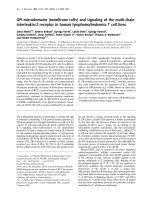
nanoparticles compared to the bulk material. Figure 1.1. shows the transition of the electronic
energy states from the continuous bands of a bulk semiconductor to discrete atomic like energy
levels in Quantum Dots, which are semiconductor NCs confined in all the three dimensions to
the order of nanometer.
To describe the origin of the quantum size effect quantitatively, the particle in a sphere model
was first proposed, with the assumption of parabolic valence band and conduction bands (Efros
and Efros, 1982; Ekimov and Efros, 1988). The electronic behavior in the bulk material can be
described by the Hamiltonian
2
2
( ) ( ) ( ) ( )
2
H r V r r E r
m
(1.2)
where
( ) ( )V r V r R
is the periodic potential well,
R
is the lattice vector.
The wave function can be expressed using the Bloch equation as
.
,,
( ) ( )
ik r
v k v k
r e u r
(1.3)
5
where
.ik r
e
is the envelope function,
,,
( ) ( )
v k v k
u r u r R
(1.4)
is the periodical Bloch function. In the particle in a sphere model, electrons and holes are
assumed to be non-relativistic spinless particles, behaving as free particles with their effective
masses, in the spherical potential well of radius
R
such that
( ) 0Vr
, if
rR
and
()Vr
, if
.rR
Neglecting Coulomb interaction, the wave function can be expanded in terms of the
product of the periodic part of the Bloch function
,
()
vk
ur
(same as that in bulk) with the envelope
function
,
3
1
()
2
( ) ( , )
()
l nl
i
nlm l m
l nl
r
Jk
R
rY
R J k
(1.5)
with
1,2,3 n
0,1,2 l
,
l m l
. Here
( , )
lm
Y
are the spherical harmonics,
l
J
are the
Bessel functions and the wave numbers
nl
k
are defined as the
th
n
non-zero root of the function
l
J
,
resulting from the continuity condition at
rR
. The respective energy Eigen values for
electrons and holes can be expressed as
2
2
,
2
,
2
eh
nl
nl
eh
k
E
mR
. (1.6)
Equation indicates that the energy of the lowest electron and hole states scales with radius
R
as
2
1
R
. This indicates that the confinement energy is inversely proportional to the square of the
particle radius
R
. The effective band gap
g
E
increases with decrease in particle radius as a result
of this quantization and is given by the expression (Brus, 1986)
2
22
,0
2
,
1.8
2
gg
eh
e
EE
m R R
(1.7)
where
,0g
E
is the band gap value of the bulk material. The last term is a small correction to the
quantization energy because of the Coulombic interaction in smaller nanocrystals.
6
In the bulk material,
R
is infinite in all the three directions which lead to small spacing of the
values in k-space or in other words, the k-space for the bulk solid is characterized by a
continuous distribution of states in all the spatial directions. In a quantum well, the particle size
is reduced along one of the dimension to a few nm, restricting the motion of electron to a plane,
with their behavior similar to two-dimensional (2D) electron gas. As a result, the wave numbers
have a quasi-continuous distribution along the plane where the electron is free to move, whereas
they are quantized along the confinement direction obeying the relation
/k n a
where
a
is
the particle size along the confined direction (Krahne et al., 2011). A number of quantum well
systems are studied till date (Mora-Ramos et al., 2006) (Knap et al., 2002; Bergman et al.,
1991; Hicks and Dresselhaus, 1993; West and Eglash, 1985). On reducing the dimensions of
the material along the two dimensions, to the order of a few nanometers, one can get quasi-1D
systems or nanowires. Nanowires of different materials have been synthesized (Huang et al.,
2001; Chan et al., 2008; Goren-Ruck et al., 2014; Kang and Vaddiraju, 2014; Xu et al., 2012).
Figure 1.1 Electronic energy states of a semiconductor in the transition from discrete
molecules to Quantum Dots (QDs) and bulk crystals. Semiconductor QDs are
characterized by discrete atomic like states with the effective band gap determined by
the radius R whereas the bulk material is characterized by continuous valence and
conduction band separated by distinct energy gap (Smith and Nie, 2009)