AN0717 building a 10 bit bridge sensing circuit using the PIC16C6XX and MCP601 operational amplifier
Bạn đang xem bản rút gọn của tài liệu. Xem và tải ngay bản đầy đủ của tài liệu tại đây (181.25 KB, 8 trang )
AN717
Building a 10-bit Bridge Sensing Circuit using the
PIC16C6XX and MCP601 Operational Amplifier
Author:
BRIDGE SENSOR DATA
ACQUISITION CIRCUIT
IMPLEMENTATION
Bonnie C. Baker
Microchip Technology Inc.
INTRODUCTION
Sensors that use Wheatstone bridge configurations,
such as pressure sensors, load cells, or thermistors
have a great deal of commonality when it comes to the
signal conditioning circuit. This application note delves
into the inner workings of the electronics of the signal
conditioning path for sensors that use Wheatstone
bridge configurations. Analog topics such as gain and
filtering circuits will be explored. This discussion is
complemented with digital issues such as digital filtering and digital manipulation techniques. Overall, this
note’s comprehensive investigation of hardware and
firmware provides a practical solution including error
correction in the data acquisition sensor system.
A sensor that is configured in a Wheatstone bridge typically supplies a low level, differential output signal. The
application problem the designer is challenged with is
to capture this small signal and eventually convert it to
a digital format that gives an 8 to 12 bit representation
of the signal.
The inexpensive design strategy shown in the block
diagram in Figure 1 uses a low pass filter prior to digitization. The conversion from analog to digital is performed with the microcontroller (MCU). The MCU used
in this circuit must have internal analog functions such
as a voltage reference and a comparator. These internal analog building blocks are used to implement a first
order modulator. This is combined with the MCU’s computing power where a digital filter can be
implemented.
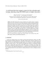
Figure 2 gives a detailed circuit for the block diagram
shown in Figure 1. The analog portion of this circuit
consists of the sensor (in this example a 1.2kΩ, 2mV/V
load cell), an analog multiplexer, an amplifier and an
R/C network. (A complete list of the load cell’s specifications is given in Table 1.) An analog multiplexer is
used to switch the two sensor outputs between a single
ended signal path to the controller. The amplifier is configured as a buffer and used to isolate the sensor load
from the R/C network. The R/C network implements the
integrator function of a first order modulator. This network can also be used to adjust the input range to the
MCU.
Rated Capacity
32 ounces (896 g)
Excitation
5VDC to 12VDC
Rated Output
2mV/V ±20%
Zero Balance
±0.3mV/V
Operating Temperature
-55 to 95°C
Compensated Temperature
-5 to 50°C
Zero Balance over Temperature
0.036% FS/°C
Output over Temperature
0.036% FS/°C
Resistance
1200Ω ±300Ω
Safe Overload
150%
Full-Scale Deflection
0.01” to 0.05”
TABLE 1: Load Cell, LCL816G (Omega)
Specifications.
LOW
MUX
PASS
FILTER
PICmicro®
FIGURE 1: The bridge sensor signal conditioning
chain filters high frequency noise in the analog domain
then immediately digitizes it with a microcontroller.
1999 Microchip Technology Inc.
DS00717A-page 1
AN717
RB0
RB1
RA3
R2
7
MAX323
3
LCP
A4
Firmware closes Loop
VSENSOR = VDD
LCN
VDD
A2
R1
—
RA0
MCP601
+
A1
CINT
A3B
RA2
VSENSOR
R1= 2.15kΩ (2.67kΩ nominal)
R2= 165kΩ
CINT= 1µF (60Hz LPF)
A1= Single Supply, CMOS op amp
A2= Single Supply Analog Multiplexer
A3= Dual Digital Pot, 1kΩ
VDD= 5V
A4 = PIC16CXX Microcontroller
Comparator
—
+
VREF3 = VSENSOR/2
(can be internal or external)
10kΩ
A3A
1µF
10kΩ
FIGURE 2: The combination of an R/C network and the microcontroller’s analog peripherals can be used to perform an
A/D conversion function.
In this circuit, the integrator function of the modulator is
implemented with an external capacitor, CINT. When
RA3 of the PIC16C6XX is set high, the voltage at RA0
increases in magnitude. This occurs until the output of
the comparator (CMCON<6>) is triggered low. At this
point, the driver to the RA3 output is switched from high
to low. Once this has transpired, the voltage at the input
to the comparator (RA0) decreases. This occurs until
the comparator is tripped high. At this point, RA3 is set
high and the cycle repeats. While the modulator section
of this circuit is cycling, two counters are used to keep
track of the time and of the number of ones versus
zeros that occur at the output of the comparator. The
firmware flow chart for this conversion process is
shown in Figure 3.
CMCON =0x03
COUNTER =0
RESULT =0
YES
NO
VREF > VRAO
RA3 =0
INCR (RESULT)
RA3 =1
INCR (COUNTER)
NO
COUNTER=1024?
YES
CMCON =0x06
DONE
FIGURE 3: This microcontroller A/D conversion flow
chart is implemented with the circuit shown in
Figure 2. Care should be taken to make the time that
every cycle takes through the flow chart constant.
DS00717A-page 2
1999 Microchip Technology Inc.
AN717
After the timing counter goes to 1024 on one side of the
Wheatstone bridge, the MCU switches the multiplexer
(A2) to the leg of the other side of the sensor. With the
voltage of the other leg of the sensor connected to the
input of the amplifier, the controller cycles through
another conversion for 1024 counts. The two results
from these cycles are subtracted, giving the conversion
results. This technique provides 10-bits of resolution
with 9.9-bits of accuracy (rms).
The design equations for this circuit are:
VIN (CM) = VREF3
VIN (P to P) = VRA3 (P to P) (R1 / R2)
with VIN (CM) approximates VDD /2 or is equal to
(LCP + LCN)/2,
where:
ERROR SOURCES AND SYSTEM
SOLUTIONS
A wheatstone bridge is designed to give a differential
output rendering a small voltage that changes proportionally to the sensor’s excitation, i.e. pressure or temperature, etc. The dominant types of errors that a
sensor exhibits in its transfer function can be categorized as offset, gain, linearity, noise, and thermal.
These sensors also produce other errors such as hysteresis, repeatability, stability and aging that are
beyond the scope of this application note. An equal
contributor to the overall system errors is the offset,
gain, and linearity errors from the active components in
the signal conditioning path.
OFFSET ERRORS
VIN (P to P) is equal to (LCP(MAX) − LCN(MIN)) or
(LCP(MIN) − LCN(MAX)) which equals the sensor full
scale range and VRA3 (P to P) is equal to VRA3 (MAX)
− VRA3 (MIN) or
approximately VDD
The system in this application note has been designed
to have a full-scale input range to the comparator of
± 40.5mV. Given 9.9-bit (rms) accuracy, the LSB size is
84.7µV.
The transfer function of the percentage of ones
counted versus input voltage is shown in Figure 4. In
this diagram, both the duty cycle between ones and
zeros as well as the pulse width is modulated.
Digital Data Stream
at the Output
of the Comparator
Voltage In
FIGURE 4: The relationship between input voltage
and the number of ones that are counted by the
controller is shown conceptually with this diagram. At
low input voltages, the output of the comparator
produces very few zeros within the 1024 counts. At
voltages in the center of the input range, the
comparator quickly toggles between ones and zeros.
At higher voltages, the comparator output produces
mostly zeros and very few ones.
1999 Microchip Technology Inc.
The offset error of a system can be mathematically
described with a constant additive to the entire transfer
function as shown in Figure 5.
5.0
4.0
Output Signal
VREF3 is the voltage reference applied to the comparator’s non-inverting input and equal to approximately VSENSOR /2. If made external, this
reference voltage can be used to adjust offset
errors
Ideal Transfer
Function
3.0
2.0
Transfer
Function with
Offset Error
1.0
0.0
0
1
2
3
4
Input Signal / Excitation
5
6
Out = Offset Error + IN
FIGURE 5: The offset error of a system can be
described graphically with a transfer function that has
shifted along the x-axis.
Typically, offset error is measured at a point where the
input signal to the system is zero. This technique provides an output signal that is equal to the offset. This
type of error can originate at the sensor or within the
various components in the analog signal path. By definition, the offset error is repeatable and stable at a
specified operating condition. If the operating conditions change, such as temperature, voltage excitation
or current excitation, the offset error may also change.
The offset errors in this signal path come from the
wheatstone bridge sensor, the operational amplifier
(A1) offset, the port leakage current at RA0, the internal
voltage reference (VREF3) offset, the comparator offset,
and the non-symmetrical output port of RA3. The only
difference in the signal path of the two sensor outputs
is the multiplexer channel, which interfaces directly with
a high impedance CMOS operational amplifier. Otherwise, both sensor output signals are configured to
travel down the same signal-conditioning path. Consequently, the conversion data taken from the positive leg
DS00717A-page 3
AN717
of the load cell sensor (LCP) has the same offset and
gain errors as the conversion data taken from the negative output of the load cell sensor (LPN), with the
exception of the bridge’s offset error.
To accommodate these errors, the design equations for
this circuit remains:
VIN (CM) = VREF3
VIN(P to P) = VRA3 (P to P) (R1 / R2)
But, now the worst case variation of VIN(P to P) is equal
to (LCP(MAX) − LCP(MIN) + LCOFF + A1OFF + RA0OFF +
VREF3-OFF + COMPOFF + RA3OFF)
where:
∆LCOFF is the maximum offset voltage that can be
generated by the load cell bridge
A1OFF is the offset voltage of the operational
amplifier
RA0OFF is the offset error caused by the leakage
current of port RA0. This leakage current is specified at 1nA at room temperature and 0.5µA (max)
over temperature. This leakage current causes a
voltage drop across the parallel combination of R1
and R2
VREF3-OFF is the offset error of the internal voltage
reference of the MCU or VDD/2. This error can be
reduced significantly with an external voltage reference
COMPOFF is the offset of the internal comparator
of the MCU and
RA3OFF is caused by the inability of RA3 to go
completely to the rails. It can be quantified by
RA3OFF = ((VDD − RA3HIGH) − RA3LOW)/2. This
formula assumes VREF3 = VDD / 2
The maximum magnitudes of these errors are summarized in Table 2.
Error Source
Offset Voltage over
Temperature
Load Cell Bridge
±1.5mV in a 5V system
Op Amp
±2mV
Port Leakage, RA0
±1.3mV
Internal VREF
±49mV
Comparator
±10mV
Output Port, RA3
(asymmetrical output
swing)
The offset errors of the circuit can be calibrated in firmware. This is performed by subtracting the conversion
code results of the positive leg of the sensor from the
results of the negative leg of the sensor. The analog
representation of the result of this calculation in firmware is:
VOUT = LCP + LCOFF + A1OFF + RA0OFF +
VREF3-OFF + COMPOFF + RA3OFF − LCN −
A1OFF − RA0OFF − VREF3-OFF − COMPOFF
− RA3OFF
VOUT = LCP − LCN + LCOFF
This result illustrates the efficiency of using firmware to
eliminate most of the offset errors, however, the
trade-off for having offset adjustments performed by
the MCU is dynamic range. In anticipation of these offset errors, the designer should increase the
peak-to-peak analog input range of the conversion system. This will result in a conversion that has a wider
dynamic range, consequently, lower accuracy.
To counteract this, the accuracy can be improved if
more samples are taken in the conversion process.
This technique will elongate the overall conversion
time. Another technique that can be used is to perform
a simple offset adjust in hardware which can be implemented with the digital potentiometer (A3A).
Hardware Offset Calibration
Given the design equations for this circuit and the
errors in Table 2, the total expected offset error over
temperature for the electronics is ±69.3mV. With a sensor full-scale range of ±10mV, the dynamic range of the
system would be ~7.9 times larger than the nominal,
error free peak-to-peak range at the input of the comparator.
The 8-bit, 1kΩ digital potentiometer (A3A) in Figure 2 is
placed in series between the power supply (5V) with
two 10kΩ, 1% resistors. This configuration provides a
voltage reference range to the comparator of ±119mV
centered around mid-supply (2.5V) with a resolution of
0.5mV. If an external reference is used with a ±0.5mV
error range, the electronics will contribute ±20.8mV offset error over temperature. This changes the worst
case full-scale peak-to-peak range of the system to
±30.8mV. This is only approximately three times larger
than the nominal full-scale output (±10mV) of the sensor.
System Span (Gain) Errors
5.5mV
TABLE 2: Maximum offset errors over temperature for
the circuit shown in Figure 3.
DS00717A-page 4
Firmware Offset Calibration
The span or gain of a system can be mathematically
described as a constant, which is multiplied against the
input signal. The magnitude of the span can easily be
determined using the formula below:
Ideal Output = Input x Gain
1999 Microchip Technology Inc.
AN717
Span error is the deviation of the span multiple from
ideal and can be described with the formula below:
Actual Output = Input x Span (1 + Span Error)
Examples of transfer functions with span error are
shown in Figure 6. The plots in Figure 6 do not have
offset errors.
5.0
Output Signal
4.0
Ideal Transfer
Function
3.0
2.0
Transfer
Function with
Span Error
1.0
0.0
0
1
2
3
4
Input Signal / Excitation
5
6
SYSTEM LINEARITY ERRORS
Linearity error differs from offset or span errors in that
it has a unique affect on each individual code of the digitizing system. Linearity errors are defined as the deviation of the transfer function from a straight line. Some
engineers define this error using a line that stretches
between the end points of the transfer curve while others define it using a line that is calculated using a “best
fit” algorithm. In either case, the linearity errors can
cause significant errors in translating the sensor input
(pressure, temperature, etc.) to digital code.
Linearity errors come in many forms as shown in
Figure 7. Sometimes the linearity error of a system can
be characterized with a multi-order polynomial, but
more typically this error is difficult to predict from system to system, in which case, firmware piecewise linearization methods are usually used.
Actual Output = Input x Span (1 + Span Error)
5.0
4.0
Output Signal
FIGURE 6: Span or gain errors can be described
graphically as a transfer function that rotates around
the intercept of the x and y-axis.
Firmware Span (Gain) Calibration
For this circuit, the span error of the sensor is less influential than the offset errors on the system. Span errors
come from the Load Cell (±20%), the resistors (±1%),
capacitor (±10%), and the ON resistance of the RA3
port (0.2%). This circuit can rely on firmware calibration
with a reduction in the dynamic range of the system.
The combination of the sensor error and the capacitor
error increases the requirements on the input range to
the modulator configuration.
Hardware Span (Gain) Calibration
Span errors can most effectively be removed in the
analog domain. For instance, the span error of the sensor can be adjusted with the sensor’s excitation voltage. As a trade-off for this adjustment strategy, the
common mode voltage of the sensor is changed, creating offset errors with respect to the reference voltage
(VREF3) of the comparator. This problem can be alleviated by making the voltage reference ratiometric to the
sensor excitation source. Span errors can also be
adjusted with either R1 or R2. In the circuit in Figure 2,
the other half of the dual, 1kΩ digital potentiometer
(A3B) is configured to perform this function. This type of
adjustment does not change the offset error of the system. Finally, span errors can be corrected with changes
to the integration capacitor. Of all of the span adjustments, this one is the most awkward to implement.
Ideal Transfer
Function
3.0
2.0
Transfer
Function with
Linearity Error
1.0
0.0
0
1
2
3
4
Input Signal / Excitation
5
6
Out = Offset + (Span x IN)(j + kIN2 + mIN3 +…)
or
Out = Offset + (Span x IN)(uncharacterized polynomial)
FIGURE 7: The linearity error of a sensor or system
can sometimes be modeled and understood, which
allows the designer to use predetermined algorithms
in the MCU to minimize their affect. However, typically,
these errors are not easily predicted and difficult to
calibrate out of the signal path.
Linearity errors in this system originate primarily in the
sensor and secondarily in the remainder of the signal
conditioning circuit.
Firmware Linearization
Linearity errors can be calibrated out of the system in
firmware using polynomial calculations if the transfer
function is understood or piecewise linearization methods if the transfer function from part to part varies. If
piecewise linearization is used, calibration data should
be taken from the system and stored in EEPROM. Utilizing the calibration data, piecewise linearization is
easily implemented using two 16 bit unsigned subtractions, one 16 bit unsigned multiplication and one 16 bit
unsigned divide.
XCAL = XFULL / (YFULL – YOFF) x (YSAMP – YZERO)
where:
XCAL is equal to the calibrated results
XFULL is the ideal full scale response saved in
EEPROM
1999 Microchip Technology Inc.
DS00717A-page 5
AN717
YFULL is the measured full scale response saved in
EEPROM
YOFF is the measured offset error saved in
EEPROM
YSAMP is the measured sample that requires linearization and calibration
This style of linearization correction also removes offset and span errors from the digital results.
Hardware Linearization
There are two components that generate linearity
errors. The sensor can contribute up to ±0.25%FS
error. The capacitor in this circuit can also contribute an
appreciable error if care is not taken in limiting the
charge and discharge range of the device. If the R/C
time constant of the circuit is greater than the inverse of
the sample frequency, the non-linearity of this time
response will cause a linearity error in the system.
In this case the R/C time constant is equal to:
tRC = R1||R2 x CINT
tRC = 2.67kΩ||165kΩ x 1µF
tRC = 2.627msec
y(n) = (2x(n) + x(n-1) + x(n-2) + x(n-3) + x(n-4) +
x(n-5) + x(n-6)) / 8
where:
n identifies the measurement sample
y(n) is the output digital results
x(n) is the measurement sample results
This filter is also known as a sinc3 filter.
Other filter types, such as the Infinite Impulse
Response (IIR) filter or a decimation filter can also be
used to improve accuracy. A detailed discussion of
these filters are beyond the scope of this application
note, however, references have been provided for further reading.
Hardware Noise Reduction
In Figure 2, the R/C network that is used to implement
the integrator function also serves as a low pass filter.
This low pass filter is equal to:
f3dB = 1 / (2 π R1 ||R2 x CINT)
Further noise reduction can be implement by adding a
second modulator stage at the input so this system.
This implementation is shown in Figure 8.
also, tRC <= tSAMPLE /6.5
The maximum voltage deviation due to the non-linearity
of the R/C network is ~10mV. This is below a 0.2%
error. If a lower sampling frequency is used, the integrating capacitor must be increased in value.
SYSTEM NOISE ERRORS
Noise can plague the best of circuits, particularly circuits that have large analog segments. An effective way
to approach noise problems is to use a basic list of
guidelines in conjunction with a working knowledge of
noise fundamentals. The checklist that every designer
should have on hand includes:
1.
2.
3.
4.
Are bypass capacitors included in the design?
Is a low impedance ground plane implemented
to minimize any ground noise across sensitive
analog parts?
Are appropriate anti-aliasing filters used in front
of the A/D converter?
Are the devices in the circuit too noisy?
Firmware Noise Reduction
The A/D converter described in this application note
was modeled after a classic first order delta-sigma
topology. In the digital domain, the data collection algorithm implements a simple average engine by default.
This style of averaging, otherwise known as digital filtering, is also called a single order sinc filter or Finite
Impulse Response (FIR) filter.
Further noise reduction algorithms can be implemented with the PIC MCU which will produce a system
with higher accuracy. As an example, a third order FIR
filter can be implemented with the following calculations in code:
DS00717A-page 6
1999 Microchip Technology Inc.
AN717
RB0
RB1
VSENSOR = VDD
Firmware
closes Loop
RA3
LCLC+
R4
7
MAX323
3
—
½
MCP602
A2
R2
—
½
MCP602
R3
CINT
+
A4
VDD
R1
RA0
+
A4
R1, R3 = 2.15kΩ (2.67kΩ nominal)
R2, R4 = 165kΩ
CINT = 1µF (60Hz LPF)
A1 = Single Supply, CMOS op amp
A2 = Single Supply Analog Multiplexer
A3 = Dual Digital Pot, 1kΩ
VDD = 5V
A4 = PIC16C6XX Microcontroller
CINT
A3B
A1
Comparator
—
RA2
VSENSOR
+
VREF3 = VSENSOR/2
(can be internal or external)
10kΩ
A3A
1µF
10kΩ
FIGURE 8: An additional modulator stages can reduce noise in the system even further. In this circuit, one modulator
stage is added which improves the system from a 9.9-bit accurate (rms) system to an 11.1-bit accurate system.
REFERENCES
Peter, Baker, Butler, Darmawaskita, “Making a
Delta-Sigma Converter Using A Microcontroller’s Analog Comparator Module”, AN700, Microchip Technology, Inc.
Baker, Bonnie C., “Anti-aliasing, Analog Filters for Data
Acquisition Systems”, AN699, Microchip Technology,
Inc.
Baker, Bonnie C., “Layout Tips for 12-Bit Converter
Applications”, AN688, Microchip Technology, Inc.
Morrison, Ralph, “Noise and Other Interfering Signals”,
John Wiley & Sons, Inc., 1192
1999 Microchip Technology Inc.
Baker, Bonnie C., “Analog Circuit Noise Sources and
Remedies”, EDTN Internet Magazine, Analog Avenue
Tech Notes, Oct. 1998
Baker, Bonnie C., “Noise Sources in Applications Using
Capacitive Coupled Isolated Products”, AB-047,
Burr-Brown Corp.
Palacheria, Amar, “Implementing IIR Digital Filters”,
AN540, Microchip Technology, Inc.
Norsworthy, Schreier, Temes, “Delta-Sigma A/D Converters: Theory, Design, and Simulation”, IEEE Press
DS00717A-page 7
WORLDWIDE SALES AND SERVICE
AMERICAS
AMERICAS (continued)
Corporate Office
Toronto
Singapore
Microchip Technology Inc.
2355 West Chandler Blvd.
Chandler, AZ 85224-6199
Tel: 480-786-7200 Fax: 480-786-7277
Technical Support: 480-786-7627
Web Address:
Microchip Technology Inc.
5925 Airport Road, Suite 200
Mississauga, Ontario L4V 1W1, Canada
Tel: 905-405-6279 Fax: 905-405-6253
Microchip Technology Singapore Pte Ltd.
200 Middle Road
#07-02 Prime Centre
Singapore 188980
Tel: 65-334-8870 Fax: 65-334-8850
Atlanta
Microchip Asia Pacific
Unit 2101, Tower 2
Metroplaza
223 Hing Fong Road
Kwai Fong, N.T., Hong Kong
Tel: 852-2-401-1200 Fax: 852-2-401-3431
Microchip Technology Inc.
500 Sugar Mill Road, Suite 200B
Atlanta, GA 30350
Tel: 770-640-0034 Fax: 770-640-0307
Boston
Microchip Technology Inc.
5 Mount Royal Avenue
Marlborough, MA 01752
Tel: 508-480-9990 Fax: 508-480-8575
Chicago
Microchip Technology Inc.
333 Pierce Road, Suite 180
Itasca, IL 60143
Tel: 630-285-0071 Fax: 630-285-0075
Dallas
Microchip Technology Inc.
4570 Westgrove Drive, Suite 160
Addison, TX 75248
Tel: 972-818-7423 Fax: 972-818-2924
Dayton
Microchip Technology Inc.
Two Prestige Place, Suite 150
Miamisburg, OH 45342
Tel: 937-291-1654 Fax: 937-291-9175
Detroit
Microchip Technology Inc.
Tri-Atria Office Building
32255 Northwestern Highway, Suite 190
Farmington Hills, MI 48334
Tel: 248-538-2250 Fax: 248-538-2260
Los Angeles
Microchip Technology Inc.
18201 Von Karman, Suite 1090
Irvine, CA 92612
Tel: 949-263-1888 Fax: 949-263-1338
New York
Microchip Technology Inc.
150 Motor Parkway, Suite 202
Hauppauge, NY 11788
Tel: 631-273-5305 Fax: 631-273-5335
San Jose
Microchip Technology Inc.
2107 North First Street, Suite 590
San Jose, CA 95131
Tel: 408-436-7950 Fax: 408-436-7955
ASIA/PACIFIC
Hong Kong
ASIA/PACIFIC (continued)
Taiwan, R.O.C
Microchip Technology Taiwan
10F-1C 207
Tung Hua North Road
Taipei, Taiwan, ROC
Tel: 886-2-2717-7175 Fax: 886-2-2545-0139
EUROPE
Beijing
United Kingdom
Microchip Technology, Beijing
Unit 915, 6 Chaoyangmen Bei Dajie
Dong Erhuan Road, Dongcheng District
New China Hong Kong Manhattan Building
Beijing 100027 PRC
Tel: 86-10-85282100 Fax: 86-10-85282104
Arizona Microchip Technology Ltd.
505 Eskdale Road
Winnersh Triangle
Wokingham
Berkshire, England RG41 5TU
Tel: 44 118 921 5858 Fax: 44-118 921-5835
India
Denmark
Microchip Technology Inc.
India Liaison Office
No. 6, Legacy, Convent Road
Bangalore 560 025, India
Tel: 91-80-229-0061 Fax: 91-80-229-0062
Microchip Technology Denmark ApS
Regus Business Centre
Lautrup hoj 1-3
Ballerup DK-2750 Denmark
Tel: 45 4420 9895 Fax: 45 4420 9910
Japan
France
Microchip Technology Intl. Inc.
Benex S-1 6F
3-18-20, Shinyokohama
Kohoku-Ku, Yokohama-shi
Kanagawa 222-0033 Japan
Tel: 81-45-471- 6166 Fax: 81-45-471-6122
Arizona Microchip Technology SARL
Parc d’Activite du Moulin de Massy
43 Rue du Saule Trapu
Batiment A - ler Etage
91300 Massy, France
Tel: 33-1-69-53-63-20 Fax: 33-1-69-30-90-79
Korea
Germany
Microchip Technology Korea
168-1, Youngbo Bldg. 3 Floor
Samsung-Dong, Kangnam-Ku
Seoul, Korea
Tel: 82-2-554-7200 Fax: 82-2-558-5934
Arizona Microchip Technology GmbH
Gustav-Heinemann-Ring 125
D-81739 München, Germany
Tel: 49-89-627-144 0 Fax: 49-89-627-144-44
Shanghai
Arizona Microchip Technology SRL
Centro Direzionale Colleoni
Palazzo Taurus 1 V. Le Colleoni 1
20041 Agrate Brianza
Milan, Italy
Tel: 39-039-65791-1 Fax: 39-039-6899883
Microchip Technology
RM 406 Shanghai Golden Bridge Bldg.
2077 Yan’an Road West, Hong Qiao District
Shanghai, PRC 200335
Tel: 86-21-6275-5700 Fax: 86 21-6275-5060
Italy
11/15/99
Microchip received QS-9000 quality system
certification for its worldwide headquarters,
design and wafer fabrication facilities in
Chandler and Tempe, Arizona in July 1999. The
Company’s quality system processes and
procedures are QS-9000 compliant for its
PICmicro® 8-bit MCUs, KEELOQ® code hopping
devices, Serial EEPROMs and microperipheral
products. In addition, Microchip’s quality
system for the design and manufacture of
development systems is ISO 9001 certified.
All rights reserved. © 1999 Microchip Technology Incorporated. Printed in the USA. 11/99
Printed on recycled paper.
Information contained in this publication regarding device applications and the like is intended for suggestion only and may be superseded by updates. No representation or warranty is given and no liability is assumed
by Microchip Technology Incorporated with respect to the accuracy or use of such information, or infringement of patents or other intellectual property rights arising from such use or otherwise. Use of Microchip’s products
as critical components in life support systems is not authorized except with express written approval by Microchip. No licenses are conveyed, implicitly or otherwise, under any intellectual property rights. The Microchip
logo and name are registered trademarks of Microchip Technology Inc. in the U.S.A. and other countries. All rights reserved. All other trademarks mentioned herein are the property of their respective companies.
1999 Microchip Technology Inc.