organic light emitting devices a survey
Bạn đang xem bản rút gọn của tài liệu. Xem và tải ngay bản đầy đủ của tài liệu tại đây (4.17 MB, 313 trang )
This is page v
Printer: Opaque this
Preface
This volume on organic light-emitting devices (OLEDs) has been written to serve
the needs of the beginning researcher in this area as well as to be a reference for
researchers already active in it.
From their very beginning, OLEDs, which include both small-molecular- and
ploymer-based devices, were recognized as a promising display technology. As
the dramatic improvements in the devices unfolded over the past two decades,
the investment of research and development resources in this field grew exponentially. The fascination with these devices is due to several potential advantages:
(1) Relative ease and low cost of fabrication, (2) their basic properties as active
light-emitters (in contrast to liquid-crystal displays, which are basically polarizing
filters requiring a backlight), (3) flexibility, (4) transparency, and (5) scalability.
Once the performance of red-to-green OLEDs approached and then exceeded that
of incandescent bulbs and fluorescent lights, it became clear that they are serious
candidates for general solid-state lighting technology, competing directly with inorganic LEDs. Hence, while inorganic LEDs are the dominant solid-state lighting
devices at present, OLEDs are expected to gradually replace the inorganic devices
in more and more niche areas. Finally, OLEDs are attracting considerable attention as building blocks for some types of molecular electronic devices, and, most
recently, for spintronic devices. In short, although their introduction into commercial products began only a few years ago, the breadth of their impact is widening
rapidly.
The first reports of electroluminescence (EL) from an organic material can be
traced back to 1907, and the first actual OLED, based on anthracene, was fabricated
vi
Preface
in 1963. However, it was not a thin-film device, and the operating voltage was
extremely high. After years of efforts to improve its performance, interest in the
subject waned. The breakthroughs that led to the exponential growth of this field
and to its first commercialized products can be traced to two poineering papers. The
1987 paper by Tang and Van Slyke demonstrated that the performance of greenemitting thin film OLEDs based on the small organic molecule tris(8-hydroxy
quinoline) Al (Alq3 ) is sufficiently promising to warrant extensive research on a
wide variety of thin film OLEDs. The 1990 paper by Bradley, Friend, and coworkers
described the first ploymer OLED (PLED), which was based on poly(p-phenylene
vinylene) (PPV), and demonstrated that such devices warrant close scrutiny as
well. Since then, the competition between small-molecular OLEDs and PLEDs
continues in parallel with the overall dramatic developments of this field. This
volume has tried to mirror this competition by devoting comparable attention to
these two subfields.
The first chapter provides an introduction to the basic physics of OLEDs and
surveys the various topics and challenges in this field. It includes a description of the
basic optical and transport processes, the materials used in some of the OLEDs that
have studied extensively to date, the performance of various blue-to-red OLEDs,
and a brief outlook.
Chapters 2 through 4 are devoted to small-molecular OLEDs. Chapter 2 focuses on design concepts for molecular materials yielding high performance small
molecular OLEDs, including the recent developments in electrophosphorescent
devices. Chapter 3 focuses on the degradation processes affecting Alq3 , which
is arguably the small molecular device material that has been studied in more
detail than any other. Chapter 4 is devoted to organic microcavity light emitting
diodes, providing a review of the geometrical effects of the OLED geometry on
its performance.
Chapters 5 through 9 are devoted to various PLEDs. Chapter 5 provides an
extensive review of devices based poly(p-phenylene vinylene), which has been
studied more than any other light-emitting polymer. Chapter 6 is devoted to the
dominant effects of polymer morphology on device performance. Chapter 7 is devoted to studies of the transient EL in PPV-based PLEDs, which exhibit EL spikes
and have provided considerable insight into details of carrier dynamics in these devices. Chapter 8 reviews the extensive work on EL of polyparaphenylenes (PPPs),
which in 1993 were the first reported blue-light emitting polymers. Although other
blue-light emitting polymers have been developed since then, notably polyfluorenes and phenyl-substituted polyacetylenes, PPPs were studied extensively and
provided extensive insight into light-emitting polymers in general and blue emitters
in particular. Chapter 9 reviews direct and alternating current light-emitting devices
based on pyridine-containing conjugated polymers. In particular, it describes the
symmetrically-configured AC light-emitters (SCALE) devices and discusses their
potential. Finally, Chapter 10 focuses on polyflurorene-based PLEDs which de-
Preface
vii
veloped during the past six years and are perhaps the most promising blue devices,
and consequently provide a basis for full-color PLED-based displays.
In spite of the fast pace of developments on OLEDs, it is hoped that the topics
provided in this volume will be valuable as tutorials for the beginning resercher
and as a desktop reference for the advanced researcher for some time to come.
Joseph Shinar
Ames, IA, February, 2003
This is page viii
Printer: Opaque this
This is page ix
Printer: Opaque this
Contents
Preface
v
Contributors
1
Introduction to Organic Light-Emitting Devices
Joseph Shinar and Vadim Savvateev . . . . . . . . . . . . . . . . .
1.1
Introduction . . . . . . . . . . . . . . . . . . . . . . . . . .
1.2
Basic Electronic Structure and Dynamics of π -Conjugated
Materials . . . . . . . . . . . . . . . . . . . . . . . . . . . .
1.3
Basic Structure of OLEDs . . . . . . . . . . . . . . . . . . .
1.4
OLED Fabrication Procedures . . . . . . . . . . . . . . . . .
1.4.1 Thermal Vacuum Evaporation . . . . . . . . . . . .
1.4.2 Wet-Coating Techniques . . . . . . . . . . . . . . .
1.5
Materials for OLEDs & PLEDs . . . . . . . . . . . . . . . .
1.5.1 Anode Materials and HTLs or Buffers . . . . . . . .
1.5.2 Small Electron-Transporting and Emitting Molecules.
1.5.3 Small Molecular Guest Dye Emitters . . . . . . . . .
1.5.4 White OLEDs . . . . . . . . . . . . . . . . . . . . .
1.5.5 Phosphorescent Small Molecules &
Electrophosphorescent OLEDs . . . . . . . . . . . .
1.5.6 Fluorescent Polymers . . . . . . . . . . . . . . . . .
1.5.7 Cathode & Organic/Cathode Buffer Materials . . . .
1.6
Basic Operation of OLEDs . . . . . . . . . . . . . . . . . .
1.7
Carrier Transport in OLEDs . . . . . . . . . . . . . . . . . .
1.7.1 Polaron vs Disorder Models for Carrier Hopping . . .
xv
.
.
1
1
.
.
.
.
.
.
.
.
.
.
5
9
10
10
11
12
12
17
18
18
.
.
.
.
.
.
19
19
21
22
23
24
x
Contents
1.7.2
1.7.3
1.7.4
Long-Range Correlations . . . . . . . . . . . .
Carrier Injection . . . . . . . . . . . . . . . . .
Space-Charge Limited Versus Injection-Limited
Current Mechanisms . . . . . . . . . . . . . .
1.8
The Efficiency of OLEDs . . . . . . . . . . . . . . . .
1.9
Degradation Mechanisms . . . . . . . . . . . . . . . .
1.10 Outlook for OLEDs . . . . . . . . . . . . . . . . . . .
References . . . . . . . . . . . . . . . . . . . . . . . . . . . .
2
3
. . . .
. . . .
25
26
.
.
.
.
.
Molecular LED: Design Concept of Molecular Materials for
High-Performance OLED
Chihaya Adachi and Tetsuo Tsutsui . . . . . . . . . . . . . . . .
2.1
Introduction . . . . . . . . . . . . . . . . . . . . . . . .
2.2
OLED Development from the 1960s to the 1980s . . . .
2.3
Working Mechanisms of OLED . . . . . . . . . . . . . .
2.3.1 Charge Carrier Injection and Transport . . . . . .
2.3.2 Carrier Recombination and Emission Process . .
2.3.3 Estimation of External and Internal Quantum
Efficiency . . . . . . . . . . . . . . . . . . . . .
2.4
Design of Multilayer Structures . . . . . . . . . . . . . .
2.5
Molecular Materials for OLED . . . . . . . . . . . . . .
2.5.1 Hole-Transport Material . . . . . . . . . . . . .
2.5.2 Electron-Transport Material . . . . . . . . . . . .
2.5.3 Emitter Material . . . . . . . . . . . . . . . . . .
2.5.4 Dopant Material . . . . . . . . . . . . . . . . . .
2.5.5 Molecular Tuning for High EL Efficiency . . . .
2.5.6 Molecular Tuning for a High EL Durable OLED .
2.6
Future Possibilities of OLED . . . . . . . . . . . . . . .
2.7
Conclusion . . . . . . . . . . . . . . . . . . . . . . . . .
References . . . . . . . . . . . . . . . . . . . . . . . . . . . . .
.
.
.
.
.
.
.
.
.
.
.
.
.
.
.
28
29
31
33
34
.
.
.
.
.
.
.
.
.
.
.
.
.
.
.
.
.
.
43
43
43
45
46
50
.
.
.
.
.
.
.
.
.
.
.
.
.
.
.
.
.
.
.
.
.
.
.
.
.
.
.
.
.
.
.
.
.
.
.
.
50
53
55
55
58
60
60
62
63
64
65
65
.
.
.
.
.
.
.
.
71
71
72
72
78
85
86
89
.
91
Chemical Degradation and Physical Aging of Aluminum(III)
8-Hydroxyquinoline: Implications for Organic Light-Emitting
Diodes and Materials Design
Keith A. Higginson, D. Laurence Thomsen III, Baocheng Yang, and
Fotios Papadimitrakopoulos . . . . . . . . . . . . . . . . . .
3.1
Introduction . . . . . . . . . . . . . . . . . . . . . . . . . .
3.2
Chemical Stability of OLED Materials . . . . . . . . . . . .
3.2.1 Thermal Hydrolysis of Alq3 . . . . . . . . . . . . .
3.2.2 Electrochemical Degradation of Alq3 and Hq . . . .
3.3
Morphological Stability of Organic Glasses in LEDs . . . . .
3.3.1 Crystallization of Alq3 . . . . . . . . . . . . . . . .
3.3.2 Guidelines for Amorphous Materials Selection . . . .
3.3.3 Crystallization and Aging of AlMq3 and
Alq3 /AlMq3 blends . . . . . . . . . . . . . . . . . .
4
5
6
Contents
xi
3.4
The Effect of Aging Processes on OLED Performance . . . . .
References . . . . . . . . . . . . . . . . . . . . . . . . . . . . . . . .
95
98
Organic Microcavity Light-Emitting Diodes
Ananth Dodabalapur . . . . . . . . . . . . . . . . . . . . . . . .
4.1
Introduction . . . . . . . . . . . . . . . . . . . . . . . . .
4.2
Types of Microcavities . . . . . . . . . . . . . . . . . . . .
4.3
Planar Microcavity LEDs . . . . . . . . . . . . . . . . . .
4.4
Single Mode and Multimode Planar Microcavity LEDs . .
4.5
Intensity and Angular Dependence in Planar Microcavities
4.6
Materials for Organic Microcavity LED Displays . . . . .
4.7
Summary . . . . . . . . . . . . . . . . . . . . . . . . . . .
References . . . . . . . . . . . . . . . . . . . . . . . . . . . . . .
.
.
.
.
.
.
.
.
.
.
.
.
.
.
.
.
.
.
103
103
104
106
110
114
121
123
124
Light-Emitting Diodes Based on Poly(p-phenylenevinylene)
and Its Derivatives
Neil C. Greenham and Richard H. Friend . . . . . . . . . . . .
5.1
Introduction . . . . . . . . . . . . . . . . . . . . . . . .
5.2
The Electronic Structure of PPV . . . . . . . . . . . . .
5.3
Synthesis of PPV and Derivatives . . . . . . . . . . . . .
5.4
Single-Layer LEDs . . . . . . . . . . . . . . . . . . . .
5.5
Multiple-Layer Polymer LEDs . . . . . . . . . . . . . .
5.6
Transport and Recombination in Polymer LEDs . . . . .
5.7
Optical Properties of Polymer LEDs . . . . . . . . . . .
5.8
Novel LED Structures . . . . . . . . . . . . . . . . . . .
5.9
Prospects for Applications of PPV-Based LEDs . . . . .
5.10 Conclusions . . . . . . . . . . . . . . . . . . . . . . . .
References . . . . . . . . . . . . . . . . . . . . . . . . . . . . .
.
.
.
.
.
.
.
.
.
.
.
.
.
.
.
.
.
.
.
.
.
.
.
.
127
127
128
132
134
138
141
143
146
149
150
150
.
.
.
.
155
155
157
157
.
.
.
.
.
.
.
.
.
161
166
166
167
172
176
180
182
182
.
.
.
.
.
.
.
.
.
.
.
.
Polymer Morphology and Device Performance in
Polymer Electronics
Yijian Shi, Jie Liu, and Yang Yang . . . . . . . . . . . . . . . . . .
6.1
Introduction . . . . . . . . . . . . . . . . . . . . . . . . . .
6.2
The Control of Polymer Morphology . . . . . . . . . . . . .
6.2.1 The Polymer–Polymer Interactions in Solutions . . .
6.2.2 The Morphology Control of Polymer Thin Films via
the Spin-Coating Process . . . . . . . . . . . . . . .
6.3
The Control of Device Performance via Morphology Control.
6.3.1 Conductivity of the Polymer Film . . . . . . . . . .
6.3.2 Charge-Injection Energy Barriers . . . . . . . . . . .
6.3.3 The Turn-on Voltages . . . . . . . . . . . . . . . . .
6.3.4 The Emission Spectrum of the Device . . . . . . . .
6.3.5 The Device Quantum Efficiency . . . . . . . . . . .
6.4
Conclusions . . . . . . . . . . . . . . . . . . . . . . . . . .
6.4.1 The Solvation Effect and Polymer Aggregation . . .
xii
Contents
6.4.2
The Device Emission Color and the Quantum
Efficiency . . . . . . . . . . . . . . . . . . . .
6.4.3 The Conductivity of the Film . . . . . . . . . .
6.4.4 The Turn-on Voltage of the PLED Device . . .
References . . . . . . . . . . . . . . . . . . . . . . . . . . . .
7
8
9
.
.
.
.
.
.
.
.
.
.
.
.
.
.
.
.
182
182
183
183
On the Origin of Double Light Spikes from Polymer Light-Emitting
Devices
Aharon Yakimov, Vadim Savvateev, and Dan Davidov . . . . . . . . .
7.1
Introduction . . . . . . . . . . . . . . . . . . . . . . . . . . .
7.2
Experimental . . . . . . . . . . . . . . . . . . . . . . . . . . .
7.3
Results and Analysis . . . . . . . . . . . . . . . . . . . . . . .
7.4
Discussion . . . . . . . . . . . . . . . . . . . . . . . . . . . .
7.5
Conclusions . . . . . . . . . . . . . . . . . . . . . . . . . . .
References . . . . . . . . . . . . . . . . . . . . . . . . . . . . . . . .
187
187
188
190
199
202
203
Electroluminescence with Poly(para-phenylenes)
Stefan Tasch, Wilhelm Graupner, and G¨unther Leising . . . . . . . .
8.1
Introduction . . . . . . . . . . . . . . . . . . . . . . . . . .
8.2
Physical Properties of Oligophenyls and Polyphenyls . . . .
8.2.1 Processing and Stability . . . . . . . . . . . . . . . .
8.2.2 Geometric Arrangement of Para-phenylenes . . . . .
8.2.3 Absorption Properties . . . . . . . . . . . . . . . . .
8.2.4 Emission Properties . . . . . . . . . . . . . . . . . .
8.2.5 Excited States . . . . . . . . . . . . . . . . . . . . .
8.2.6 Charge Transport . . . . . . . . . . . . . . . . . . .
8.3
Electroluminescence . . . . . . . . . . . . . . . . . . . . . .
8.3.1 Single-Layer LED Based on PPP-Type Polymers . .
8.3.2 Emission Colors . . . . . . . . . . . . . . . . . . . .
8.3.3 LEDs Based on Multilayer Structures . . . . . . . .
8.3.4 LEDs Based on Polymer Blends . . . . . . . . . . .
8.3.5 Light-Emitting Electrochemical Cells Based on PPPs.
8.4
Conclusions . . . . . . . . . . . . . . . . . . . . . . . . . .
References . . . . . . . . . . . . . . . . . . . . . . . . . . . . . . .
.
.
.
.
.
.
.
.
.
.
.
.
.
.
.
.
.
205
205
206
206
208
209
214
214
217
220
220
224
225
229
233
238
238
Direct and Alternating Current Light-Emitting Devices Based on
Pyridine-Containing Conjugated Polymers
Y. Z. Wang, D. D. Gebler, and A. J. Epstein . . . . . . . . . . . . . . .
9.1
Introduction . . . . . . . . . . . . . . . . . . . . . . . . . . .
9.2
Experiments . . . . . . . . . . . . . . . . . . . . . . . . . . .
9.3
Results and Discussion . . . . . . . . . . . . . . . . . . . . .
9.4
Summary and Conclusion . . . . . . . . . . . . . . . . . . . .
References . . . . . . . . . . . . . . . . . . . . . . . . . . . . . . . .
245
245
247
249
261
262
Contents
10 Polyfluorene Electroluminescence
Paul A. Lane . . . . . . . . . . . . . . . . . . . . . . . . .
10.1 Introduction . . . . . . . . . . . . . . . . . . . . .
10.2 Synthesis and Characterization of Polyfluorene . . .
10.2.1 Polyfluorene Synthesis . . . . . . . . . . .
10.2.2 Optical and Physical Characterization . . .
10.2.3 Electronic Characterization . . . . . . . . .
10.3 Electroluminescence . . . . . . . . . . . . . . . . .
10.3.1 Polyfluorene Electroluminescence . . . . .
10.3.2 Fluorene-Based Copolymers . . . . . . . .
10.3.3 Doped Polyfluorene Light-Emitting Diodes
10.4 Concluding Remarks . . . . . . . . . . . . . . . .
References . . . . . . . . . . . . . . . . . . . . . . . . . .
Index
.
.
.
.
.
.
.
.
.
.
.
.
.
.
.
.
.
.
.
.
.
.
.
.
.
.
.
.
.
.
.
.
.
.
.
.
.
.
.
.
.
.
.
.
.
.
.
.
.
.
.
.
.
.
.
.
.
.
.
.
xiii
.
.
.
.
.
.
.
.
.
.
.
.
265
265
266
266
268
270
275
275
282
288
298
299
303
This is page xiv
Printer: Opaque this
This is page xv
Printer: Opaque this
Contributors
Editor:
Joseph Shinar, Ames Laboratory – USDOE & Department of Physics and
Astronomy, Iowa State University, Ames, IA
Chapter 1:
Joseph Shinar, Ames Laboratory – USDOE & Department of Physics and
Astronomy, Iowa State University, Ames, IA
Vadim Savvateev, 3M Corporate Research Center, St. Paul, MN
Chapter 2:
Chihaya Adachi, Department of Photonics Materials Science, Chitose Institute of
Science & Technology (CIST), Chitose, Japan
Tetsuo Tsutsui, Department of Materials Science and Technology, Graduate School
of Engineering Sciences, Kyushu University, Kasuga, Fukuoka, Japan
Chapter 3:
Fotis Papadimitrakopoulos, Department of Chemistry and Institute of Materials
Science, University of Connecticut, Storrs, CT
Baocheng Yang, Department of Chemistry and Institute of Materials Science,
University of Connecticut, Storrs, CT
Keith Higginson, Triton Systems Inc., Chelmsford, MA
D. Laurence Thomsen III, NASA Landley Research Center, Hampton, VA
xvi
Contributors
Chapter 4:
Ananth Dodabalapur, Department of Electrical and Computer Engineering, Microelectronics Research Center, The University of Texas at Austin, Austin,
TX
Chapter 5:
Neil C. Greenham, Cavendish Laboratory, Cambridge University, Cambridge, UK
Richard H. Friend, Cavendish Laboratory, Cambridge University, Cambridge, UK
Chapter 6:
Yang Yang, Department of Material Science and Engineering, University of
California, Los Angeles, CA
Yijian Shi, Department of Materials Science and Engineering, University of
California, Los Angeles, CA
Jie Liu, General Electric Global Research, Niskayuna, NY
Chapter 7:
Aharon Yakimov, GE Global Research Center, Niskayuna, NY 12309
Vadim Savvateev, 3M Corporate Research Center, St. Paul, MN
Dan Davidov, Racah Institute of Physics, The Hebrew University, Jerusalem, Israel
Chapter 8:
Stefan Tasch, Institut f¨ur Festkorpephysik, Technische Universitt Graz, Austria
Wilhelm Graupner, Austriamicrosystems AG, Schloss Premstaetten, Austria
Guenther Leising, Institut f¨ur Festkorpephysik, Technische Universit¨at Graz,
Austria
Chapter 9:
Arthur J. Epstein, Department of Physics, Department of Chemistry, and Center
for Materials Research, The Ohio State University, Columbus, OH
D. Gebler, The Ohio State University, Columbus, OH
Y. Z. Wang, The Ohio State University, Columbus, OH
Chapter 10:
Paul A. Lane, Draper Laboratory, Cambridge, MA
This is page 1
Printer: Opaque this
1
Introduction to Organic Light-Emitting
Devices
Joseph Shinar and Vadim Savvateev
1.1
Introduction
Using organic materials for light-emitting devices (LEDs) is fascinating due to
their vast variety and the relative ease of controlling their composition to tune
their properties by chemical means. The first organic electroluminescence (EL)
cells were fabricated and studied in an ac mode in 1953 by Bernanose et al.,1
and in a dc mode in 1963 by Pope and coworkers.2 Soon after ac EL was also
achieved using an emissive polymer.3 The observation of bright EL with an external
quantum efficiency ηext , defined as the number of photons emitted from the face
of the device per injected electron or hole, of 4–6% in anthracene crystals with
powdered graphite electrodes marked another milestone.4 However, single-crystal
anthracene-based organic LEDs (OLEDs) were thick and hence required very high
operating voltages. The fabrication of bright green multilayer thin film devices
based on tris-(8-hydroxy quinoline) Al (Alq3 ), which yielded ηext ∼ 1%,5 spawned
a period of intense research and development, on both small molecular OLEDs
and polymer LEDs (PLEDs), which continues to grow at a fast rate.6,7,8 Figure 1.1
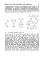
shows the molecular structures of some small molecules widely used in OLEDs;
Figure 1.2 shows the structures of some π -conjugated and other polymers. Figure
1.3 shows several photoluminescence (PL) spectra of films and EL spectra of
OLEDs based on these molecules.9−12
2
J. Shinar and V. Savvateev
FIGURE 1.1. Molecular structure of widely used π-conjugated small molecules: (a) tris(8-hydroxy quinoline Al) (Alq3 ); (b) rubrene (5,6,11,12-tetraphenyl tetracene or 5,6,11,12tetraphenyl naphthacene); (c) copper phthalocyanine, (CuPc); (d) N, N -diphenyl-N, N bis(3-methylphenyl)-1,1 -biphenyl-4, 4 -diamine (TPD); (e) N, N -diphenyl-N, N -bis(1naphthylphenyl)-1, 1 -biphenyl-4, 4 -diamine (NPB, α-NPB, NPD, or α-NPD); (f) 4, 4 , 4 tris(diphenyl amino)triphenylamines (TDATAs); (g) 4, 4 -bis(2, 2 -diphenylvinyl)-1, 1 biphenyl (DPVBi).
The work on Alq3 and other small π -conjugated molecules that followed shortly
thereafter13,14 demonstrated that multilayer OLEDs could be fabricated simply by
thermal evaporation of these molecules. In 1990 Friend and coworkers described
the first PLED,15 in which the luminescent poly(p-phenylene vinylene) (PPV)
1. Introduction to Organic Light-Emitting Devices
3
FIGURE 1.2. Molecular structure of widely used π-conjugated and other polymers: (a)
poly(para-phenylene vinylene) (PPV); (b) σ (solid line along backbone) and π (“clouds”
above and below the σ line) electron probability densities in PPV; (c) poly(2-methoxy5-(2’-ethyl)-hexoxy-1,4-phenylene vinylene) (MEH-PPV); (d) polyaniline (PANI): (d.1)
leucoemeraldine base (LEB), (d.2) emeraldine base (EB), (d.3) pernigraniline base
(PNB); (e) poly(3,4-ethylene dioxy-2,4-thiophene)-polystyrene sulfonate (PEDOT-PSS);
(f) poly(N -vinyl carbazole) (PVK); (g) poly(methyl methacrylate) (PMMA); (h) methylbridged ladder-type poly(p-phenylene) (m-LPPP); (i) poly(3-alkyl thiophenes) (P3ATs);
(j) polyfluorenes (PFOs); (k) diphenyl-substituted trans-polyacetylenes (t-(CH)x ) or
poly(diphenyl acetylene) (PDPA).
4
J. Shinar and V. Savvateev
FIGURE 1.3. The photoluminescence (PL) and electroluminescence (EL) spectra of some
representative π-conjugated films and OLEDs, respectively: (a) EL of blue aminooxadiazole fluorene (AODF) and green Alq3 OLEDs,9 (b) PL and EL of PPV films and PLEDs,
respectively,10 (c) PL of m-LPPP films, (d) EL of DPVBi (solid line) and DPVBi/Alq3
(dashed line) OLEDs,11 and (e) PL of CBP films and EL of CBP OLEDs.12
was fabricated by spin-coating a precursor polymer onto the transparent conducting indium-tin-oxide (ITO) anode substrate, thermally converting the precursor
to PPV, and finally evaporating the Al thin film cathode on the PPV. The developments in both small molecular OLEDs and PLEDs since the seminal reports
1. Introduction to Organic Light-Emitting Devices
5
of Tang and VanSlyke and of Friend and coworkers have been truly spectacular:
from very dim devices with a lifetime of less than 1 minute in air, to green OLEDs
that can operate continuously for over 20,000 hours (833 days) at a brightness
of 50–100 Cd/m2 (i.e., comparable to a typical TV or computer monitor),16 or
in pulsed operation at >106 Cd/m2 ,17 or blue, white, and red devices with continuous dc lifetimes of over 2000 hours. Indeed, the developments have been so
remarkable, that serious effort is now underway towards the most ubiquituos application: replacing the incandescent and fluorescent light bulbs with OLEDs as
the primary source for general lighting applications. However, even as they now
enter the marketplace,18,19 outstanding challenges in the efficiency and long-term
degradation processes of OLEDs remain. These are intimately tied to the dynamics of the basic excitations in these materials and devices, namely singlet excitons
(SEs), triplet excitons (TEs), and p− and p + polarons, to which the electrons and
holes, respectively, relax as they are injected from the electrode into the organic
layer of the OLED. This chapter reviews the basic properties of these devices,
including the basic photophysics of these excitations.
1.2
Basic Electronic Structure and Dynamics of
π-Conjugated Materials
Most luminescent organic molecules are π-conjugated compounds, i.e., materials
in which single and double or single and triple bonds alternate throughout the
molecule or polymer backbone. The second and third bonds of a double or triple
bond are π bonds, i.e., if the backbone of the molecule or polymer is along the x
axis, then the orbitals which define these π bonds are formed from overlapping
atomic pz or py orbitals. Since the energy of electrons in π orbitals is usually higher
than in the σ orbitals (which are generated from sp 3 , sp 2 , or sp hybridized atomic
orbitals), the gap between the highest occupied molecular π orbital (HOMO) and
the lowest unoccupied molecular π ∗ orbital (LUMO) is typically in the 1.5–3 eV
range, i.e., the materials are semiconductors.20 Due to the overlap of π orbital
wave functions of adjacent carbon atoms, the electrons occupying such orbitals
are relatively delocalized. Figure 1.2(b) shows the π electron clouds in PPV, which
are generated from electrons in the overlapping atomic pz orbitals. Since these pz
orbitals have lobes above and below the x-y plane of the σ bonds of PPV, the
π electrons lie above and below this plane. Although it is not reflected in Fig.
1.2(b), the distance between two C atoms is shorter and the π electron cloud
between them is more dense in the double C C than in the single C–C bond.
The difference between these distances, or, equivalently, between the densities of
the π electrons in the double vs. the single bond, is a measure of the “alternation
parameter,” and it may strongly impact the electronic structure of the molecule or
polymer.21,22
Due to the π conjugation, in the perfect isolated polymer chain the delocalized
π electron cloud extends along the whole length of the chain. However, in the
6
J. Shinar and V. Savvateev
real chain various defects, such as external impurities (e.g., H, O, Cl, or F atoms
which eliminate the double bond, etc.) or intrinsic defects (e.g., kinks, torsional
conformations, a cross-link with a neigboring chain, etc.) break the conjugation.
In the typical polymer film, the length of a conjugated segment typically varies
from ∼5 repeat units to ∼15 repeat units. The HOMO-LUMO gap decreases with
increasing conjugation length to an asymptotic value usually reached at ∼10 repeat
units.21
An important characteristic of both polymer and small molecular films is disorder. Although polymer chains may be quite long, typically the π -conjugation
is interrupted by topological defects. Hence the conjugated polymers can be considered as an assembly of conjugated segments. The length of the segments is
subject to random variation that is a major source of energetic disorder implying both inhomogeneous broadening of the absorption spectrum and a relatively
broad density-of-states (DOS) energy distribution for neutral and charged excitations. However, the structural disorder in amorphous films of small π -conjugated
molecules also leads to a similarly broad DOS distribution. The width of the DOS
of the charge transport manifold, to a large degree, determines the charge transport characteristics of the material (see Sec. 1.7 below). Due to the broad DOS
distribution, the tail states of this distribution can in principle act as the shallow
trapping states for charge carriers at low temperatures (intrinsic localized states).
On the other hand, extrinsic trapping, meaning the presence of localized states that
differ from the majority of hopping states in that they require a larger energy to
release the charge carriers back to the intrinsic DOS, is also possible.
The ground state of most of the luminescent molecules and polymers which are
used as the emitters in OLEDs and PLEDs is the symmetric singlet 11 Ag state.22
Figure 1.4 shows the basic processes which may occur following photoexcitation of
the molecule or conjugated segment of the polymer. Since the material is assumed
to be luminescent, the antisymmetric 11 Bu state must lie below the symmetric 2photon 21 Ag state. Otherwise, photoexcitation will still populate the 11 Bu state, but
that state will quickly decay to the 21 Ag , and the latter will decay nonradiatively
to the ground state, with lifetimes as short as ∼2 ps.23
As Figure 1.4 shows, several processes may occur following photoexcitation of
the molecule or conjugated segment of the polymer into the vibrational manifold
of the 11 Bu :
(1) Rapid (∼100 fs) thermalization of the excited state to the lowest 11 Bu vibrational state, followed by radiative decay to the ground state. The radiative
lifetime is typically ∼ 1 ns.20,24,25
(2) Charge transfer from the 11 Bu to an adjacent molecule or segment of a chain,
i.e., dissociation of the 11 Bu . This process may also be extremely fast.24 Indeed, so fast that it has been suspected that this charge transfer state, aka a
“spatially indirect exciton,” “charge transfer exciton (CTE),” or “intermolecular or interchain polaron pair,” may be generated directly from the ground
state.24
1. Introduction to Organic Light-Emitting Devices
7
FIGURE 1.4. Basic processes following photoexcitation of a π-conjugated molecule or
polymer.
(3) Intersystem crossing (ISC) from the 11 Bu to the lowest state in the triplet
manifold, assumed to be the 13 Bu . Although the yield of this ISC process is known to be high in some specific molecules, e.g., anthracene20 and
C60 ,26 it is apparently very low in most π -conjugated molecules and polymers. In some unusual cases such as solid rubrene (5,6,11,12-tetraphenyl
tetracene or 5,6,11,12-tetraphenyl naphthacene; see Figure 1.1), where the
energy E(11 Bu ) of the 11 Bu is about twice the energy E(13 Bu ) of the lowest
triplet, the 11 Bu dissociates to two 13 Bu triplets on neighboring molecules
with a very high yield. This process quenches the PL yield of solid rubrene
films down to ∼ 10%. In contrast, the PL yield of dilute rubrene solutions is
∼100%.27
The dynamics of the polarons and TEs, and their interactions with the SEs, have
been the subject of numerous studies.20−25 ,28−36 Although the source of the EL is
the recombination of a polaron pair in the antisymmetric singlet configuration to
a SE:
p− + p + → 1 S ∗ → 11 Bu + phonons → hν + phonons,
(1)
a polaron pair in the symmetric singlet configuration or the triplet configuration
may recombine to a TE:
p − + p + → 3 T ∗ → 13 Bu + phonons.
(2)
Indeed, spin statistics mandate that if the rates of reactions (1) and (2) are the
same, then the nongeminate polaron pairs generated by carrier injection in OLEDs
would yield 3 TEs for every SE. This SE/TE branching ratio is one of the most
important factors suppressing the efficiency of OLEDs based on the fluorescent
decay of SEs. However, recent studies suggest that in luminescent π -conjugated
polymers the rate of reaction (1) is higher than that of (2), so the yield of SEs is
8
J. Shinar and V. Savvateev
higher than 25%.37 While it may be as high as 50% in PPV-based PLEDs,38 it may
even be higher in most of the other PLEDs.38 The issue of efficiency of OLEDs is
treated in some detail in Sec. 1.8.
The copious generation of TEs in OLEDs (Eq. (2)) has motivated the recent successful development of OLEDs based on electrophosphorescence, i.e.,
on the radiative decay of TEs in molecules containing a heavy transition metal
or rare-earth atom, where that decay is partially allowed due to strong spin-orbit
coupling.40,41,42 Although in the most recent study42 it was shown that some of
the emission was due to triplet-triplet annihilation to SEs,
13 Bu + 13 Bu → 1 S ∗ → 11 Bu + phonons → hν + phonons,
(3)
it appears that in general this process is marginal in most π -conjugated polymer
films, as well as both PLEDs and small molecular OLEDs, probably due to the
strong localization and low diffusivity of TEs in these disordered systems.30,34,35
As mentioned in point (ii) above, the 11 Bu SEs may decay nonradiatively by
dissociating into an interchain or intermolecular polaron pair. This dissociation
may be induced by an external electric field,32 defects such as carbonyl groups
(which, in PPV, are generated by photooxidation),25 charged defects as may be
found in the organic/organic or organic/cathode interfaces in OLEDs, or any other
species generating an electric field. Hence, besides their recombination to singlet
and triplet excitons, polarons may play another major role in π -conjugated films
and OLEDs: Since they generate an electric field, they may also quench SEs:
p−/+ + 11 Bu → p−/+∗ + phonons
(4)
p −/+ + 11 Bu → p−/+ + p + + p − + phonons.
(5)
or
Indeed, considerable evidence for such quenching of SEs by polarons has accumulated over the past decade,29−31 and recent modeling of the behavior of multilayer
OLEDs43 and optically detected magnetic resonance (ODMR) studies suggest that
this quenching process may be a major mechanism in suppressing the efficiency
of OLEDs, in particular at high injection current of OLEDs.29 It should be noted,
however, that in small molecular OLEDs it is believed that the quenching of SEs
by polarons does not result in dissociation of the SE but rather in absorption of its
energy by the polaron (Eq. 4).20 Finally, TEs may quench the SEs as well,20 and
that mechanism may indeed be responsible for the triplet resonances observed in
ODMR studies of these materials.28−30
The foregoing section attempted to provide an introduction to the dynamics of
singlet excitons, generated either by photoexcitation or by polaron recombination,
and the effects of polarons and TEs on the SE dynamics. We now turn to the basic
structure and dynamics of OLEDs, which obviously reflect the basic processes
described above.
1. Introduction to Organic Light-Emitting Devices
9
FIGURE 1.5. Basic structure of a bilayer OLED.
1.3
Basic Structure of OLEDs
The basic structure of a typical dc-biased bilayer OLED is shown in Figure 1.5.
The first layer above the glass substrate is a transparent conducting anode, typically
indium tin oxide (ITO). Flexible OLEDs, in which the anode is made of a transparent conducting organic compound, e.g., doped polyaniline (see Fig. 1.2),44 or
poly(3,4-ethylene dioxy-2,4-thiophene) (PEDOT)-polystyrene sulfonate (PEDOTPSS) (see Fig. 1.2)45 deposited on a suitable plastic, e.g., transparency plastic, have
also been reported.
The single- or multi-layer small organic molecular or polymer films are deposited on the transparent anode. Appropriate multilayer structures typically
enhance the performance of the devices by lowering the barrier for hole injection from the anode and by enabling control over the e− − h+ recombination
region, e.g., moving it from the organic/cathode interface, where the defect density is high, into the bulk. Hence, the layer deposited on the anode would generally
be a good hole transport material, providing the hole transport layer (HTL). Similarly, the organic layer in contact with the cathode would be the optimized electron
transporting layer (ETL).
10
J. Shinar and V. Savvateev
The cathode is typically a low-to-medium workfunction (φ) metal such as
3.66 eV)5
Ca (φ
2.87 eV), Al (φ
4.3 eV),15 or Mg0.9 Ag0.1 (for Mg, φ
deposited either by thermal or e-beam evaporation. However, in case of Al or Ca,
addition of an appropriate buffer layer between the top organic layer and the metal
cathode improves the device performance considerably. This issue is discussed in
some detail in Sec. 1.5.8 below.
1.4
OLED Fabrication Procedures
The existing OLED fabrication procedures fall into two major categories: (1) thermal vacuum evaporation of the organic layers in small molecular OLEDs, and (2)
wet coating techniques of the polymer layers in PLEDs.
1.4.1
Thermal Vacuum Evaporation
Thermal evaporation of small molecules is usually performed in a vacuum of
∼10−6 torr or better. However, it has been observed that the residual gases in the
chamber may affect the performance of the devices significantly. For example,
Br¨omas et al.47 found that the performance of OLEDs in which a Ca film was
deposited as the cathode in a high vacuum (HV; ∼10−6 torr) system was far better
than that of OLEDs deposited under ultra-high vacuum (UHV; ∼10−10 torr). This
was apparently due to the formation of an oxide buffer layer between the top organic
layer and the metal cathode and, indeed, led to the deliberate introduction of an
AlOx buffer layer by Li et al.48 In another case, it was found that Au/[organic]/Au
device structures were rectifying when deposited under HV but symmetric when
fabricated under UHV.49
One of the most salient advantages of thermal vacuum evaporation is that it
enables fabrication of multilayer devices in which the thickness of each layer
can be controled easily, in contrast to spin coating (see below). In addition, 2dimensional combinatorial arrays of OLEDs, in which two parameters (e.g., the
thickness or composition of two of the layers) may be varied systematically across
the array, can be relatively easily fabricated in a single deposition procedure.50,12
This combinatorial fabrication greatly enhances the efficiency of systematic device
fabrication aimed at optimizing the various parameters.
The major appeal of vacuum deposition techniques is that they employ the
generally available vacuum equipment existing in the semiconductor industry.
Using properly matched shadow masks for depositing RGB emitting materials
allows a relatively simple way to achieve multi-color displays in segmented-color,
active-matrix (AM) full color, and passive-matrix (PM) configurations. The commercial Pioneer vehicular stereo OLED display (1999) and Motorola cell phone
OLED display (2000) were prepared with Kodak-licensed small molecule vacuum
sublimation technology.
1. Introduction to Organic Light-Emitting Devices
1.4.2
11
Wet-Coating Techniques
General remarks and spin-coating
Since polymers generally crosslink or decompose upon heating, they cannot be
thermally evaporated in a vacuum chamber (in case of PPVs, rapid photooxidation
is an additional problem as even residual quantities of oxygen lead to significant emission quenching). Hence, they are generally deposited by wet-coating a
thin film from a solution containing them. That, however, imposes restrictions on
the nature of the polymers and the sidegroups attached to the polymer backbone,
since the polymer must be soluble. For example, unsubstituted PPV (Fig. 2) is
insoluble. Hence, it is generally fabricated by spin-coating a soluble precursor
polymer onto the desired substrate (typically ITO). The precursor polymer film
is then converted to PPV by annealing at a temperature 150 ≤ T ≤ 250◦ C for
up to ∼24 hours.15,34,51,52 As this conversion process yields an insoluble layer
of PPV, additional layers may be deposited on it by spin-coating.51,52 However,
when soluble PPV derivatives such as 2,5-dialkoxy PPVs are spun-coated onto
the substrate, only solvents which would not redissolve the deposited film can
be used to deposit additional layers. Thus, Gustaffson et al.44 fabricated flexible PLEDs by sequentially spin-coating an aqueous solution of water-soluble,
conducting transparent polyaniline onto a transparency, and a xylene solution of
poly(2-methoxy-5-(2’-ethyl)-hexoxy-1,4-phenylene vinylene) (MEH-PPV) (see
Fig. 1.2).
Although the thickness of spun-coated films may be controlled by the concentration of the polymer in the solution, the spinning rate, and the spin-coating
temperature, it is difficult to fabricate thick films and the thickness obviously
cannot be monitored during deposition. In addition, no combinatorial fabrication
methods have been developed for spun- coated PLEDs (see above).
Spin-coating is an established procedure in the semiconductor and display industries, widely used in photolithography of silicon and ITO and polycrystalline
backplanes for liquid-crystal displays. However it may not be used for large size
single plane displays for rapid web coating in reel-to-reel processes desired in
flexible display manufacturing. An even more important limitation of spin-coating
is that it does not provide a way to pattern full-color display. The whole surface
of the substrate is covered with the light-emitting polymer, and the devices are
created through cathode patterning.
Doctor blade technique
In this technique, a film of the solution containing the soluble polymer is spread
with uniform thickness over the substrate using a precision “doctor blade.”53 In
contrast to spin-coating, the doctor-blade technique is very useful for fabricating
relatively thick films, but does not enable the fabrication of films <100 nm thick,
which are commonly used in OLEDs.
12
J. Shinar and V. Savvateev
Wet-Casting
An important development of wet-casting is inkjet printing, achieved by Yang
and coworkers.54 It is currently being utilized for the development of organic
high-information content (HIC) displays by, e.g., Cambridge Display Technology,
Seiko-Epson,55 and Philips.56 This technique is currently leading the pursuit for
commercially viable HIC displays, as the organic layers are deposited directly as
an array of pixels. While several companies have announced the development of
ink-jet printed displays, the numerous intricacies of this technique are delaying
the commercialization of PLEDs. As in the case of spin-coating, when used for
patterning bilayer PLEDs, wet casting techniques impose an additional demand of
mutual insolubility of organic layers.
Other important techniques currently studied in the area of wet casting are screen
printing, micro-stamping, and hot microprint contact.57
1.5
Materials for OLEDs & PLEDs
The list of materials that have been incorporated in OLEDs is now too large to
provide in this introductory chapter. The following list highlights some of the
materials that have drawn considerable attention:
1.5.1
Anode Materials and HTLs or Buffers
Indium–Tin–Oxide (ITO)
In the most common “cathode on top” device configuration the OLED is prepared on a glass substrate pre-coated with ITO. The ITO-coated backplane is an
established component in the LC-display industry with very large well-developed
facilities dedicated to its preparation and handling. The availability of these elaborate facilities, each of which reflects a minimal investment of as much as $400m,
is an important prerequisite for OLED penetration of the existing flat-panel display (FPD) market. The fact that these facilities were not in place when the early
attempts were made to introduce the inorganic EL displays contributed to their
failure to enter the display market. The initial cost models for OLEDs manufacturing are all built on the assumption of low cost of retooling the LCD manufacturing
facilities based on patterning and handling of ITO backplanes.58 The commercial
batches of ITO-coated glass are normally characterized by square or sheer resistance, material roughness, and layer transparency.59 All of these parameters have
important implications for device functionality and durability. However, it should
be emphasized that ITO is a non-stoichiometric mixture of In, In2 O, InO, In2 O3 ,
Sn, SnO, and SnO2 (it is sometimes even referred to as “In-doped tin oxide” or vice
versa). It also appears that the workfunction φITO of ITO films, typically ∼4.5 eV,
increases with the O content up to ∼5.1 eV. It was found that device brightness
and efficiency tend to increase with increased φITO . Hence several procedures
1. Introduction to Organic Light-Emitting Devices
13
for saturating the O content of ITO have been developed. The most common is
UV-ozone treatment, in which the ITO film is exposed to ozone produced by a
UV lamp.60 Other procedures involve partial etching of the ITO in aquaregia61 or
plasma etching.62 However, since the excess oxygen typically evolves out of the
treated ITO within a few hours, the organic layers must be deposited promptly on
the ITO after the treatment.
Using ITO-coated glass in the common configuration is problematic in several
respects. One of them is strong coupling of the emitted light to the evanescent mode
inside the glass that leads to extremely high light losses. Therefore, an alternative
“anode on top” configuration has also been developed.63 We return to this issue
below, when discussing device optimization.
Polyaniline (PANI; see Fig. 1.2)
The development of water-soluble-transparent-conducting-doped-PANI, enabled
the first fabrication of an “all plastic” PLED.44 In an interesting development of
this anode, a mixture of an aqueous solution containing the PANI and an organic
solution containing polystyrene was spun coated to yield a film, from which the
polystyrene was then etched by an organic solvent, resulting in a highly porous
PANI anode.64 The high contact area between the anode and the emitting polymer
layer enhanced h+ injection, resulting in improved device performance.
Poly(3,4-ethylene dioxy-2,4-thiophene)-polystyrene sulfonate (PEDOT-PSS; see
Fig. 1.2)65
This polymer is also water soluble, and hence, similar to PANI, can be used as a
transparent anode.
Pt
Since Pt has a very high φ
5.6 eV, it could strongly enhance hole injection.
However, since it must be very thin to be transparent, it would be deposited on,
e.g., the conventional ITO. Indeed, Malliaras et al.66 have very recently shown that
a thin layer (≤10 ˚A) of Pt on ITO enhances hole injection by up to a factor of 100
relative to the uncoated ITO.
ZnO
Although ZnO also forms transparent conducting films, it has drawn surprisingly
little attention for use as the anode in OLEDs.
On top of the ITO layer one usually deposites an HTL or more-recently “buffer”
layer. It serves to planarize the irregularities present at the ITO surface, produces
an interface with an emitting layer that confines charge carriers away from the
electrodes, and provides the h+ delivery for exciton formation.