chuyển đổi DCDC buck converters và boost converters
Bạn đang xem bản rút gọn của tài liệu. Xem và tải ngay bản đầy đủ của tài liệu tại đây (1.53 MB, 55 trang )
NPTEL – Electrical Engineering – Introduction to Hybrid and Electric Vehicles
Module 4: DC-DC Converters
Lec 9: DC-DC Converters for EV and HEV Applications
DC-DC Converters for EV and HEV Applications
Introduction
The topics covered in this chapter are as follows:
EV and HEV configuration based on power converters
Classification of converters
Principle of Step Down Operation
Buck Converter with RLE Load
Buck Converter with RL Load and Filter
Electric Vehicle (EV) and Hybrid Electric Vehicle (HEV) Configurations
In Figure 1 the general configuration of the EV and HEV is shown. Upon examination of
the general configurations it can be seen that there are two major power electronic units
DC-DC converter
DC-AC inverter
Figure 1:General Configuration of a Electric Vehicle [1]
Joint initiative of IITs and IISc – Funded by MHRD
Page 1 of 55
NPTEL – Electrical Engineering – Introduction to Hybrid and Electric Vehicles
Usually AC motors are used in HEVs or EVs for traction and they are fed by inverter and
this inverter is fed by DC-DC converter (Figure 1). The most commonly DC-DC
converters used in an HEV or an EV are:
Unidirectional Converters: They cater to various onboard loads such as sensors,
controls, entertainment, utility and safety equipments.
Bidirectional Converters: They are used in places where battery charging and
regenerative braking is required. The power flow in a bi-directional converter is
usually from a low voltage end such as battery or a supercapacitor to a high
voltage side and is referred to as boost operation. During regenerative braking,
the power flows back to the low voltage bus to recharge the batteries know as
buck mode operation.
Both the unidirectional and bi-directional DC-DC converters are preferred to be isolated
to provide safety for the lading devices. In this view, most of the DC-DC converters
incorporate a high frequency transformer.
Classification of Converters
The converter topologies are classified as:
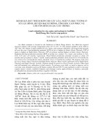
Buck Converter: In Figure 2a a buck converter is shown. The buck converter is
step down converter and produces a lower average output voltage than the dc
input voltage.
Boost converter: In Figure 2b a boost converter is shown. The output voltage is
always greater than the input voltage.
Buck-Boost converter: In Figure 2c a buck-boost converter is shown. The
output voltage can be either higher or lower than the input voltage.
Joint initiative of IITs and IISc – Funded by MHRD
Page 2 of 55
NPTEL – Electrical Engineering – Introduction to Hybrid and Electric Vehicles
S1
D1
L
eL
i1
Vin
D1
iL
R
Vin
L
i0
S1
C
R
E
Figure 2a: General Configuration Buck Converter
Figure 2b: General Configuration Boost Converter
Figure 2c: General Configuration Buck-Boost Converter
Joint initiative of IITs and IISc – Funded by MHRD
Page 3 of 55
V0
NPTEL – Electrical Engineering – Introduction to Hybrid and Electric Vehicles
Principle of Step Down Operation
The principle of step down operation of DC-DC converter is explained using the circuit
shown in Figure 3a. When the switch S1 is closed for time duration T1 , the input voltage
Vin appears across the load. For the time duration T2 is switch S1 remains open and the
voltage across the load is zero. The waveforms of the output voltage across the load are
shown in Figure 3b.
vout
S1
+
+
Vin
vout
R
-
Vin
Vin
-
t
T2
T1
T1
T
Figure 3a: Step down operation
Figure 3b: Voltage across the load resistance
The average output voltage is given by
T
Voavg
T
1 1
vout dt 1 Vin fTV
1 in DVin
T 0
T
(1)
The average load current is given by
I oavg
Voavg
R
DVin
R
(2)
Where
T is the chopping period
D
T1
is the duty cycle
T
f is the chopping frequency
The rms value of the output voltage is given by
1/ 2
Vorms
1 DT 2
vout dt
T 0
DVin
Joint initiative of IITs and IISc – Funded by MHRD
(3)
Page 4 of 55
NPTEL – Electrical Engineering – Introduction to Hybrid and Electric Vehicles
In case the converter is assumed to be lossless, the input power to the converter will be
equal to the output power. Hence, the input power ( Pin ) is given by
Pin
2
Vin2
1 DT
1 DT vout
v
i
dt
dt
D
out out
T 0
T 0 R
R
(4)
The effective resistance seen by the source is (using equation 2)
V
R
Reff in
I oavg D
(5)
The duty cycle D can be varied from 0 to 1 by varying T1 , T or f . Thus, the output
voltage Voavg can be varied from 0 to Vin by controlling D and eventually the power flow
can be controlled.
The Buck Converter with RLE Load
The buck converter is a voltage step down and current step up converter. The two modes
in steady state operations are:
Mode 1 Operation
In this mode the switch S1 is turned on and the diode D1 is reversed biased, the current
flows through the load. The time domain circuit is shown in Figure. The load current, in
s domain, for mode 1 can be found from
Ri1 ( s) sLi1 ( s)
E Vin
LI 01
s
s
(6)
U= Ldi/dt
Where
I 01 is the initial value of the current and I 01 I1 .
i1
Vin
R
L
bien doi laplace:
df(t)/dt PF(P)
i1
R
L
E
E
Figure 4: Time domain circuit of buck converter in mode 1
Joint initiative of IITs and IISc – Funded by MHRD
Figure 5: Time domain circuit of buck converter in mode 2
Page 5 of 55
NPTEL – Electrical Engineering – Introduction to Hybrid and Electric Vehicles
From equation 6, the current i1 ( s) is given by
i1 s
(Vin E )
LI1
s( R sL) R sL
(7)
In time domain the solution of equation 7 is given by
i1 (t ) I1etR / L
Vin E
1 etR / L
R
(8)
The mode1 is valid for the time duration 0 t T1 0 t DT . At the end of this mode,
the load current becomes
i1 (t T1 DT ) I 2
(9)
Mode 2 Operation
In this mode the switch S1 is turned off and the diode D1 is forward biased. The time
domain circuit is shown in Figure 5. The load current, in s domain, can be found from
Ri2 ( s) sLi2 (s)
E
LI 02
s
(10)
Where
I 02 is the initial value of load current.
The current at the end of mode1 is equal to the current at the beginning of mode 2.
Hence, from equation 9 I 02 is obtained as
I 02 I 2
(11)
Hence, the load current is time domain is obtained from equation 10 as
E
1 etR / L
R
Determination of I1 and I 2
i2 (t ) I 2etR / L
(12)
At the end of mode 2 the load current becomes
i2 (t T2 (1 D)T ) I3
(13)
At the end of mode 2, the converter enters mode 1 again. Hence, the initial value of
current in mode 1 is
(14)
I 01 I3 I1
From equation 8 and equation 12 the following relation between I1 and I 2 is obtained
as
Vin E
1 e DTR / L
R
E
I 3 I1 I 2e(1 D )TR / L 1 e(1 D )TR / L
R
I 2 I1e DTR / L
(15)
Joint initiative of IITs and IISc – Funded by MHRD
(16)
Page 6 of 55
NPTEL – Electrical Engineering – Introduction to Hybrid and Electric Vehicles
Solving equation 15 and equation 16 for I1 and I 2 gives
I1
Vin e Da 1 E
R eD 1 R
(17)
I2
Vin e Da 1 E
R e D 1 R
(18)
Where
a
TR R
L
fL
(19)
where f is the chopping frequency.
Current Ripple
The peak to peak current ripple is given by
I I 2 I1
Vin 1 e Da e a e (1 D ) a Vin 1 e Da e a e (1 D ) a
R
1 e a
fL
a 1 e a
(20a)
In case fL R , a 0 . Hence, for the limit a 0 equation 20 becomes
I
Vin D(1 D)
fL
(20b)
To determine the maximum current ripple ( I max ), the equation 20a is differentiated
w.r.t. D . The value of I max is given by
I max
Vin
R
tanh
R
4 fL
(21)
For the condition 4 fL R ,
R
R
tanh
4 fL 4 fL
(22)
Hence, the maximum current ripple is given by
I max
Vin
4 fL
(23)
If equation 20b is used to determine the maximum current ripple, the same result is
obtained.
Joint initiative of IITs and IISc – Funded by MHRD
Page 7 of 55
NPTEL – Electrical Engineering – Introduction to Hybrid and Electric Vehicles
Continuous and Discontinuous Conduction Modes
In case of large off time, particularly at low switching frequencies, the load current may
be discontinuous, i.e. i2 (t T2 (1 D)T ) will be zero. The necessary condition to ensure
continuous conduction is given by
I1 0
Vin e Da 1 E
0
R eD 1 R
(24)
E e 1
Vin e D 1
Da
The Buck Converter with R Load and Filter
The output voltage and current of the converter contain harmonics due to the switching
action. In order to remove the harmonics LC filters are used. The circuit diagram of the
buck converter with LC filter is shown in Figure 6. There are two modes of operation as
explained in the previous section.
The voltage drop across the inductor in mode 1 is
eL f Vin Vo L f
diL
and iL isw
dt
(25)
where iL is the current through the inductor L f
isw is the current through the switch
The switching frequency of the converter is very high and hence, iL changes linearly.
Thus, equation 25 can be written as
eL Vin Vo L f
iL
i
Lf L
Ton
DT
(26)
where Ton is the duration for which the switch S remains on
T is the switching time period
Joint initiative of IITs and IISc – Funded by MHRD
Page 8 of 55
NPTEL – Electrical Engineering – Introduction to Hybrid and Electric Vehicles
Vin
Lf
isw
iL
eL
V0
T2
T1
t
T
Vc
Vin
R
Vin
I2
iL
I1
t
Vin
Figure 6: Buck converter with resistive load and filter
Figure 7: Voltage and current waveform
Hence, the current ripple iL is given by
iL
Vin Vo DT
(27)
Lf
When the switch S is turned off, the current through the filter inductor decreases and the
current through the switch S is zero. The voltage equation is
diL
di
Lf D
dt
dt
where iD is the current through the diode D
Vo L f
(28)
Due to high switching frequency, the equation 28 can be written as
Vo L f
iL
iL
Lf
Toff
(1 D)T
(29)
where Toff is the duration in which switch S remains off the diode D conducts
Neglecting the very small current in the capacitor C f , it can be seen that
io isw for time duration in which switch S conducts
and
io iD for the time duration in which the diode D conducts
The current ripple obtained from equation 29 is
iL
(1 D)T
Vo
L
(30)
The voltage and current waveforms are shown in Figure 7.
Joint initiative of IITs and IISc – Funded by MHRD
Page 9 of 55
NPTEL – Electrical Engineering – Introduction to Hybrid and Electric Vehicles
From equation 27 and equation 30 the following relation is obtained for the current
ripple
iL
Vin Vo DT (1 D)T V
Lf
Lf
(31)
o
Hence, from equation 31 the relation between input and output voltage is obtained as
Vo DVin
Vo
D
Vin
(32)
If the converter is assumed to be lossless, then
Pin Po Vinisw Voio Vinisw DVinio isw Dio
(33)
The switching period T can be expressed as
Vo iL
iL
i
1
T Ton Toff L f
Lf L Lf
f
Vin Vo
Vo
Vo Vin Vo
(34)
From equation 34 the current ripple is given by
V V V
iL o in o
L f Vo f
(35)
Substituting the value of Vo from equation 32 into equation 35 gives
iL
Vin D 1 Do
(36)
fL f
Using the Kirchhoff’s current law, the inductor current iL is expressed as
iL ic io
(37)
If the ripple in load current ( io ) is assumed to be small and negligible, then
iL ic
(38)
The incremental voltage Vc across the capacitor ( C f ) is associated with incremental
charge Q by the relation
Vc
Q f
(39)
Cf
The area of each of the isoceles triangles representing Q in Figure 7 is given by
1 T iL T iL
22 2
8
Combining equation 39 and equation 40 gives
T iL
Vc
8C f
Q f
Joint initiative of IITs and IISc – Funded by MHRD
(40)
(41)
Page 10 of 55
NPTEL – Electrical Engineering – Introduction to Hybrid and Electric Vehicles
Substituting the value of iL from equation 31 into equation 41 gives
Vc
T Vin D 1 D Vin D(1 D)
8C f
fL f
8L f C f f 2
(42)
Boundary between Continuous and Discontinuous Conduction
The inductor ( iL ) and the voltage drop across the inductor ( eL ) are shown in Figure 8.
I LB I oB
eL
iL , peak
iL
I LB ,max
TVin
8L f
iLB ioB
t
T1
T2
T
Figure 8: The inductor voltage and current waveforms
for discontinuous operation
0
0.5
D
1
Figure 9: Current versus duty ratio keeping input voltage constant.
Being at the boundary between the continuous and the discontinuous mode, the inductor
current iL goes to zero at the end of the off period. At this boundary, the average inductor
current is (B rferes to the boundary)
T
1
DT
I LB iL, peak on Vin Vo
Vin Vo I oB
2
2L f
2L f
(43)
Hence, during an operating condition, if the average output current ( I L ) becomes less
than I LB , then I L will become discontinuous.
Discontinuous Conduction Mode with ConstantInput Voltage Vin
In applications such as speed control of DC motors, the input voltage ( Vin ) remains
constant and the output voltage ( Vo ) is controlled by varying the duty ratio D . Since
Vo DVin , the average inductor current at the edge of continuous conduction mode is
obtained from equation 43 as
TV
I LB in D 1 D
2L f
Joint initiative of IITs and IISc – Funded by MHRD
(44)
Page 11 of 55
NPTEL – Electrical Engineering – Introduction to Hybrid and Electric Vehicles
In Figure 9 the plot of I LB as a function of D , keeping all other parameters constant, is
shown. The output current required for a continuous conduction mode is maximum at
D 0.5 and by substituting this value of duty ration in equation 44 the maximum
current ( I LB ,max ) is obtained as
TVin
(45)
8L
From equation 44 and equation 45, the relation between I LB and I LB ,max is obtained as
I LB ,max
I LB 4I LB,max D(1 D)
(46)
To understand the ratio of output voltage to input voltage ( Vo / Vin ) in the discontinuous
mode, it is assumed that initially the converter is operating at the edge of the continuous
conduction (Figure 7), for given values of T , L,Vd and D . Keeping these parameters
constant, if the load power is decreased (i.e., the load resistance is increased), then the
average inductor current will decrease. As is shown in Figure 10, this dictates a higher
value of Vo than before and results in a discontinuous inductor current.
V0
Vin
iL , peak
iL
eL
D 1
Vin V0
I L I0
t
Discontinuous
V0
D 0.1
1T
DT
I0
I LB ,max
2T
T
Figure 10: Discontinuous operation is buck converter
Figure 11: Buck converter characteristics for constant input
current
In the time interval 2T the current in the inductor L f is zero and the power to the load
resistance is supplied by the filter capacitor alone. The inductor voltage eL during this
time interval is zero. The integral of the inductor voltage over one time period is zero and
in this case is given by
V
D
(47)
Vin Vo DT Vo 1Ts 0 o
Vin D 1
Joint initiative of IITs and IISc – Funded by MHRD
Page 12 of 55
NPTEL – Electrical Engineering – Introduction to Hybrid and Electric Vehicles
In the interval 0 t 1Ts (Figure 10) the current ripple in L f is
eL L f
diL
i
eL L f L
dt
1T
(48)
From Figure 10 it can be seen that
iL iL, peak (since the current falls)
(49)
eL Vo
(50)
Substituting the values of iL and eL from euqation 49 and equation 50 into equation 48
gives
Vo L f
iL , peak
1T
I o iL , peak
iL , peak
Vo
1T
Lf
(51)
D 1
2
VoTs
D 1 1 (from eq.51)
2L f
(52)
VinT
D1 (from eq.47)
2L f
4 LLB ,max D1 (from eq.45)
Hence, 1
Io
4 LLB ,max D
(53)
From equation 47 and equation 53 the ratio Vo / Vin is obtained as
Vo
D2
(54)
Vin D 2 1 I / I
o LB,max
4
In Figure 11 the step down characteristics in continuous and discontinuous modes of
operation is shown. In this figure the voltage ratio ( Vo / Vin ) is plotted as a function of
I o / I LB ,max for various duty ratios using equation 32 and equation 54. The boundary
between the continuous and the discontinuous mode, shown by dashed line in Figure 11,
is obtained using equation 32 and equation 48.
Joint initiative of IITs and IISc – Funded by MHRD
Page 13 of 55
NPTEL – Electrical Engineering – Introduction to Hybrid and Electric Vehicles
Discontinuous-Conduction Mode with Constant Vo
In some applications such as regulated dc power supplies, Vin may vary but Vo is kept
constant by adjusting the duty ratio. From equation 44 the average inductor current at the
boundary of continuous conduction is obtained as
TV
I LB o 1 D
(56)
2L f
From equation 56 it can be seen that, for a given value of Vo the maximum value of I LB
occurs at D 0 and is given by
TV
I LB ,max o
2L f
(57)
From equation 56 and equation 57 the relation between I LB and I LB ,max is
I LB (1 D) I LB,max
(58)
From equation 52, the output current is obtained as
VT
I o o D 1 1
2L f
(59)
I LB ,max D 1 1 (from eq.57)
Solving the equation 59 for 1 and substituting its value in equation 47 gives
Io
Vo I LB ,max
D
Vin 1 Vo
Vin
References:
1
2
(60)
[1] M. Ehsani, Modern Electric, Hybrid Electric and Fuel Cell Vehicles: Fundamentals,
Theory and Design, CRC Press, 2005
Suggested Reading:
[1] M. H. Rashid, Power Electronics: Circuits, Devices and Applications, 3rd edition,
Pearson, 2004
Joint initiative of IITs and IISc – Funded by MHRD
Page 14 of 55
NPTEL – Electrical Engineering – Introduction to Hybrid and Electric Vehicles
Lecture 10: Boost and Buck-Boost Converters
Boost and Buck-Boost Converters
Introduction
The topics covered in this chapter are as follows:
Principle of Step-Up Operation
Boost Converter with Resistive Load and EMF Source
Boost Converter with Filter and Resistive Load
Buck-Boost Converter
Principle of Step-Up Operation (Boost Converter)
The circuit diagram of a step up operation of DC-DC converter is shown in Figure 1.
When the switch S1 is closed for time duration t1 , the inductor current rises and the energy
is stored in the inductor. If the switch S1 is openerd for time duration t2 , the energy stored
in the inductor is transferred to the load via the didode D1 and the inductor current falls.
The waveform of the inductor current is shown in Figure 2.
D1
L
iL
eL
eL
Vin
iL
i0
IL
Vin
S1
C
R
t
V0
Vin V0
T1
T2
T
Figure 1:General Configuration of a Boost Converter
Figure 2: Inductor current waveform
When the switch S1 is turned on, the voltage across the inductor is
di
dt
The peak to peak ripple current in the inductor is given by
V
I s T1
L
vL L
Joint initiative of IITs and IISc – Funded by MHRD
(1)
(2)
Page 15 of 55
NPTEL – Electrical Engineering – Introduction to Hybrid and Electric Vehicles
The average output voltage is
v0 Vs L
T
I
1
Vs 1 1 Vs
T2
1 D
T2
(3)
From Equation 3 the following observations can be made:
The voltage across the load can be stepped up by varying the duty ratio D
The minimum output voltage is Vs and is obtained when D 0
The converter cannot be switched on continupusly such that D 1 . For values of
D tending to unity, the output becomes very sensitive to changes in D
For values of D tending to unity, the output becomes very sensitive to changes in (Fig.3).
D1
L
V0
eL
i0
iL
V0
R
S1
Vin
Vin
C
E
0
0.6
Figure 3: Output voltage vs. Duty ration for Boost
Converter
D
Figure 4: Boost converter with resistive load and emf source
Boost Converter with Resistive Load and EMF Source
A boost converter with resistive load is shown in Figure 4. The two modes of operation
are:
Mode 1: This mode is valid for the time duration
0 t DT
(4)
where D is the duty ratio and T is the switching period.
The mode 1 ends at t DT .
Joint initiative of IITs and IISc – Funded by MHRD
Page 16 of 55
NPTEL – Electrical Engineering – Introduction to Hybrid and Electric Vehicles
In this mode the switch S1 is closed and the equivalent circuit is shown in Figure 5. The
current rises throught the inductor L and switch S1 . The current in this mode is given by
Vs L
di
i1
dt
(5)
Since the time instants involved are very small, the term dt t . Hence, the solution of
Equation 5 is
Vs
(6)
t I1
L
where I1 is the initial value of the current. Assuming the current at the end of mode 1(
i1 (t )
t DT ) to be I 2 ( i1 (t DT ) I 2 ), the Equation 6 can be written as
I2
Vs
DT I1
L
eL
eL
iL
iL
(7)
R
C
Vin
R
Vin
E
E
Figure 5: Configuration of a Boost Converter in mode 1
C
Figure 6: Configuration of a Boost Converter in mode 2
Mode2: This mode is valid for the time duration
DT t T
(8)
In this mode the switch S1 is open and the inductor current flows through the RL load and
the equivalent circuit is shown in Figure 6. The voltage equation in this mode is given by
Vs Ri2 L
di2
E
dt
(9)
For an initial current of I 2 , the solution of Equation 9 is given by
i2 (t )
R
R
t
t
Vs E
L
1
e
I
e
2 L
L
(10)
The current at the end of mode 2 is equal to I1 :
i2 t (1 D)t I 2
Vs E
1 e (1 D ) z I 2e (1 D ) z
L
(11)
where z TR / L
Joint initiative of IITs and IISc – Funded by MHRD
Page 17 of 55
NPTEL – Electrical Engineering – Introduction to Hybrid and Electric Vehicles
Solving Equation 7 and Equation 11 gives the values of I1 and I 2 as
I1
Vs Dz e (1 D ) z
V E
s
(1 D ) z
R 1 e
R
(12)
I2
Vs Dz
V E
1
s
(1 D ) z
R 1 e
R
(13)
The ripple current is given by
I I 2 I1
Vs
DT
L
(14)
The above equations are valid if E Vs . In case E Vs , the converter works in
discontinuous mode.
Boost Converter with Filter and Resistive Load
A circuit diagram of a Buck with filter is shown in Figure 7. Assuming that the inductor
current rises linearly from I1 to I 2 in time t1
Vin L
I 2 I1
I
I
L
t1
L
t1
t1
Vin
(15)
D
S1
io
Vin
iL
L
C
R
Vo
Figure 7: Configuration of a Buck Boost Converter
The inductor current falls linearly from I 2 to I1 in time t2
Vin Vo L
I
I
t2 L
t2
Vo Vin
(16)
where I I 2 I1 is the peak to peak ripple current of inductor L . From equation 15 and
equation 16 it can be seen that
V t V V t
I in 1 o in 2
L
L
Joint initiative of IITs and IISc – Funded by MHRD
(17)
Page 18 of 55
NPTEL – Electrical Engineering – Introduction to Hybrid and Electric Vehicles
Substituting t1 DT and t2 (1 D)T gives the average output voltage
Vo Vin
V
V
T
in (1 D) in
t2 1 D
Vo
Substituting D
t1
(18)
t1
t1 f into equation 18 gives
T
Vo Vin
Vo f
(19)
If the boost converter is assumed to be lossless then
Vin Iin Vo Io Vin I o /(1 D)
Ia
1 D
The switching period T is given by
ILVo
1
I
I
T t1 t2 L
L
f
Vin
Vo Vin Vin Vo Vin
I in
From equation 22 the peak to peak ripple current is given by
V V V
V D
I in o in I in
fLVo
fL
(20)
(21)
(22)
(23)
When the switch S is on, the capacitor supplies the load current for t t1 . The average
capacitor current during time t1 is I c I o and the peak to peak ripple voltage of the
capacitor is
It
1 t1
1 t1
I
dt
I o dt a 1
c
0
0
C
C
C
Substituting the value of t1 from equation 19 into equation 24 gives
Vc vc vc (t 0)
Vc
I o Vo Vs
Vo fC
Vc
Io D
fC
(24)
(25)
Condition for Continuous Inductor Current and Capacitor Voltage
If I L is the average inductor current, the inductor ripple current is I 2I L . Hence, from
equation 18 and equation 23 the following expression is obtained
DVin
2Vin
2I L 2Io
fL
(1 D) R
The critical value of the inductor is obtained from equation 26 as
D(1 D) R
L
2f
Joint initiative of IITs and IISc – Funded by MHRD
(26)
(27)
Page 19 of 55
NPTEL – Electrical Engineering – Introduction to Hybrid and Electric Vehicles
If Vc is the averag capacitor voltage, the capacitor ripple voltage Vc 2Va . Using
equation 25 the following expression is obtained
Io D
2Va 2 I o R
Cf f
(28)
Hence, from equation 28 the critical value of capacitance is obtained as
D
C
2 fR
(29)
Buck-Boost Converter
The general configuration of Buck-Boost converter is shown Figure 7. A buck-boost
converter can be obtained by cascade connection of the two basic converters:
the step down converter
the step up converter
The circuit operation can be divided into two modes:
During mode 1 (Figure 8a), the switch S1 is turned on and the diode D is
reversed biased. In mode 1 the input current, which rises, flows through
inductor L and switch S1 .
In mode 2 (Figure 8b), the switch S1 is off and the current, which was flowing
through the inductor, would flow through L, C, D and load. In this mode the
energy stored in the inductor ( L ) is transferred to the load and the inductor
current ( iL ) falls until the switch S1 is turned on again in the next cycle.
The waveforms for the steady-state voltage and current are shown in Figure 9.
iin
id
Vin
iL
io
Figure 8a: Buck Boost Converter in mode 1
Joint initiative of IITs and IISc – Funded by MHRD
L
iL
C
L
C
R
io
Figure 8b: Buck Boost Converter in mode 2
Page 20 of 55
NPTEL – Electrical Engineering – Introduction to Hybrid and Electric Vehicles
VD
Vin
t
Vin
iL
I2
Vd is the voltage across the diode
I1
id is the current through the diode
iD
t
iL is the current through the inductor
I2
T1
t
T2
Figure 9: Current and voltage waveforms of Buck Boost Converter
Buck-Boost Converter Continuous Mode of Operation
Since the switching frequency is considered to be very high, it is assumed that the current
through the inductor ( L ) rises linearly. Hence, the relation of the voltage and current in
mode 1 is given by
I I
I
Vin L 2 1 L
T1
T1
(29)
I
T1 L
Vin
The inductor current falls linearly from I 2 to I1 in mode 2 time T2 and is given by
Vo L
I
T2
I
T2 L
Vo
(30)
The term I ( I 2 I1 ) , in mode 1 and mode 2, is the peak to peak ripple current through
the inductor L . From equation 29 and equation 30 the relation between the input and
output voltage is obtained as
VT
VT
(31)
I in 1 o 2
L
L
The relation between the on and off time, of the switch S1 , and the total time duration is
given in terms of duty ratio ( D) as:
T1 DT
(32a)
T2 1 D T
(32b)
Joint initiative of IITs and IISc – Funded by MHRD
Page 21 of 55
NPTEL – Electrical Engineering – Introduction to Hybrid and Electric Vehicles
Substituting the values of T1 and T2 from equation 32a and equation 32b into equation
31 gives:
V D
Vo in
1 D
If the converter is assumed to be lossless, then
Vin I in Vo I o
Vin I in
Vin D
I D
I o I in o
1 D
1 D
The switching period T obtained from equation 29 and equation 30 as:
V V
I
I
T T1 T2 L
L
LI in o
Vo
Vin
VinVo
(33)
(34)
(35)
The peak to peak ripple current I is obtained from equation 35 as
TVinVo
V D
DT
I
Vin in
L Vo Vin
L
fL
where
f switching frequency
(36)
When the switch S1 is turned on, the filter capacitor supplies the load current for the time
duration T1 . The average discharge current of the capacitor I cap I out and the peak to peak
ripple current of the capacitor are:
IT I D
1 T1
1 T1
Vcap I cap dt I o dt o 1 o
(37)
0
0
C
C
C
fC
Buck-Boost Converter Boundary between Continuous and Discontinuous Conduction
In Figure 10 the voltage and load current waveforms of at the edge of continuous
conduction is shown. In this mode of operation, the inductor current (iL ) goes to zero at
the end of the off interval (T2 ) . From Figure 10, it can be seen that the average value of
the inductor current is given by
1
1
I LB I 2 I
2
2
Substituting the value of I from equation 36 into equation 38 gives:
1 DT
I LB
Vin
2 L
In terms of output voltage, equation 39 can be written as
1T
I LB
Vo 1 D
2L
Joint initiative of IITs and IISc – Funded by MHRD
(38)
(39)
(40)
Page 22 of 55
NPTEL – Electrical Engineering – Introduction to Hybrid and Electric Vehicles
The average value of the output current is obained substituting the value of input current
from equation 34 into equation 40 as:
1T
2
(41)
I OB
Vo 1 D
2L
Most applications in which a buck-boost converter may be used require that Vout be kept
constant. From equation 40 and equation 41 it can be seen that I LB and I OB result in
their maximum values at D 0 as
TV
I LB ,max out
2L
TVout
I OB ,max
2L
From equation 38 it can be seen that peak-to-peak ripple current is given by
I 2I LB
(42)
(43)
Vin
t
Vin
T1
T2
I 2 I L, peak
I LB
t
Figure 10: Current and voltage waveforms of Buck Boost Converter in boundary between continuous and discontinuous mode
Suggested Reading:
[1] M. H. Rashid, Power Electronics: Circuits, Devices and Applications, 3rd edition,
Pearson, 2004
Joint initiative of IITs and IISc – Funded by MHRD
Page 23 of 55
NPTEL – Electrical Engineering – Introduction to Hybrid and Electric Vehicles
Lecture 11: Multi Quadrant DC-DC Converters I
Multi Quadrant DC-DC Converters I
Introduction
The topics covered in this chapter are as follows:
Converter classification
Two Quadrant Converters
Converter Classification
DC-DC converters in an EV may be classified into unidirectional and bidirectional
converters. Unidirectional converters are used to supply power to various onboard loads
such as sensors, controls, entertainment and safety equipments. Bidirectional DC-DC
converters are used where regenerative braking is required. During regenerative braking
the power flows back to the voltage bus to recharge the batteries.
The buck, boost and the buck-boost converters discussed so far allow power to flow
from the supply to load and hence are unidirectional converters. Depending on the
directions of current and voltage flows, dc converters can be classified into five types:
First quadrant converter
Second quadrant converter
First and second quadrant converter
Third and fourth quadrant converter
Four quadrant converter
Among the above five converters, the first and second quadrant converrters are
unidirectional where as the first and second, third and fourthand four quadrant
converters are bidirectional converters. In Figure 1 the relation between the load or
output voltage Vout and load or output current I out for the five types of converters is
shown.
v
v
v
Vout
Vout
Vout
I out i
First Quadrant
I out
i
Second Quadrant
Joint initiative of IITs and IISc – Funded by MHRD
I out
i
First and Second Quadrant
Page 24 of 55
NPTEL – Electrical Engineering – Introduction to Hybrid and Electric Vehicles
v
v
Vout
I out
I out
I out i
Vout
I out i
Vout
Third and Fourth Quadrant
Four Quadrant
Figure 1: Possible converter operation quadrants.
Second Quadrant Converter
The second quadrant chopper gets its name from the fact that the flow of current is from
the load to the source, the voltage remaining positive throughout the range of operation.
Such a reversal of power can take place only if the load is active, i.e., the load is capable
of providing continuous power output. In Figure 2 the general configuration of the
second quadrant converter consisting of a emf source in the load side is shown. The emf
source can be a separately excited dc motor with a back emf of E and armature resistace
and inductance of R and L respectively.
D
L
Io
io
R
I2
I1
Vin
S4
Vo
t
E
Vin
DT
Figure 2: Second Quadrant DC-DC Converter
T
D 1 T
t
Figure 3: Current and voltage waveform
The load current flows out of the load. The load voltage is positive but the load current is
negative as shown in Figure 2. This is a single quadrant converter but operates in the
second quadrant. In Figure 2 it can be seen that switch S 4 is turned on, the voltage E
drives current through inductor L and the output voltage is zero. The instantaneous
output current and output voltage are shown in Figure 3. The system equation when the
switch S 4 is on (mode 1) is given by
0L
dio
Rio E
dt
Joint initiative of IITs and IISc – Funded by MHRD
(1)
Page 25 of 55