Timer trong PLC 22x
Bạn đang xem bản rút gọn của tài liệu. Xem và tải ngay bản đầy đủ của tài liệu tại đây (52.94 KB, 6 trang )
S7–200 Quick Reference Information
A
To help you find information more easily, this section summarizes the following information:
- Special Memory Bits
- Descriptions of Interrupt Events
- Summary of S7–200 CPU Memory Ranges and Features
- High–Speed Counters HSC0, HSC1, HSC2, HSC3, HSC4, HSC5
- S7–200 Instructions
Table A–1 Special Memory Bits
Special Memory Bits
SM0.0 Always On SM1.0 Result of operation = 0
SM0.1 First Scan SM1.1 Overflow or illegal value
SM0.2 Retentive data lost SM1.2 Negative result
SM0.3 Power up SM1.3 Division by 0
SM0.4 30 s off / 30 s on SM1.4 Table full
SM0.5 0.5 s off / 0.5 s on SM1.5 Table empty
SM0.6 Off 1 scan / on 1 scan SM1.6 BCD to binary conversion error
SM0.7 Switch in RUN position SM1.7 ASCII to hex conversion error
1
Nummern für Bilder in der Form: Bild A
Nummern für Tabellen: Tabelle A
Chapter Number: A
S7–200 Programmable Controller System Manual
Table A–2 Interrupt Events in Priority Order
Event Number Interrupt Description Priority Group Priority in Group
8 Port 0: Receive character Communications
(highest)
0
9 Port 0: Transmit complete 0
23 Port 0: Receive message complete 0
24 Port 1: Receive message complete 1
25 Port 1: Receive character 1
26 Port 1: Transmit complete 1
19 PTO 0 complete interrupt Discrete (middle) 0
20 PTO 1 complete interrupt 1
0 I0.0, Rising edge 2
2 I0.1, Rising edge 3
4 I0.2, Rising edge 4
6 I0.3, Rising edge 5
1 I0.0, Falling edge 6
3 I0.1, Falling edge 7
5 I0.2, Falling edge 8
7 I0.3, Falling edge 9
12 HSC0 CV=PV (current value = preset value) 10
27 HSC0 direction changed 11
28 HSC0 external reset 12
13 HSC1 CV=PV (current value = preset value) 13
14 HSC1 direction input changed 14
15 HSC1 external reset 15
16 HSC2 CV=PV 16
17 HSC2 direction changed 17
18 HSC2 external reset 18
32 HSC3 CV=PV (current value = preset value) 19
29 HSC4 CV=PV (current value = preset value) 20
30 HSC4 direction changed 21
31 HSC4 external reset 22
33 HSC5 CV=PV (current value = preset value) 23
10 Timed interrupt 0 Timed (lowest) 0
11 Timed interrupt 1 1
21 Timer T32 CT=PT interrupt 2
22 Timer T96 CT=PT interrupt 3
Table A–3 Summary of S7–200 CPU Memory Ranges and Features
Description CPU 221 CPU 222 CPU 224 CPU 226 CPU 226XM
User program size 2 Kwords 2 Kwords 4 Kwords 4 Kwords 8 Kwords
User data size 1 Kwords 1 Kwords 2.5 Kwords 2.5 Kwords 5 Kwords
Process–image input register I0.0 to I15.7 I0.0 to I15.7 I0.0 to I15.7 I0.0 to I15.7 I0.0 to I15.7
Process–image output register Q0.0 to Q15.7 Q0.0 to Q15.7 Q0.0 to Q15.7 Q0.0 to Q15.7 Q0.0 to Q15.7
Analog inputs (read only) -- AIW0 to AIW30 AIW0 to AIW62 AIW0 to AIW62 AIW0 to AIW62
Analog outputs (write only) -- AQW0 to AQW30 AQW0 to AQW62 AQW0 to AQW62 AQW0 to AQW62
Variable memory (V) VB0 to VB2047 VB0 to VB2047 VB0 to VB5119 VB0 to VB5119 VB0 to VB10239
Local memory (L)
1
LB0 to LB63 LB0 to LB63 LB0 to LB63 LB0 to LB63 LB0 to LB63
Bit memory (M) M0.0 to M31.7 M0.0 to M31.7 M0.0 to M31.7 M0.0 to M31.7 M0.0 to M31.7
Special Memory (SM) SM0.0 to SM179.7 SM0.0 to SM299.7 SM0.0 to SM549.7 SM0.0 to SM549.7 SM0.0 to SM549.7
2
Read only SM0.0 to SM29.7 SM0.0 to SM29.7 SM0.0 to SM29.7 SM0.0 to SM29.7 SM0.0 to SM29.7
Timers
Retentive on–delay 1 ms
10 ms
100 ms
On/Off delay 1 ms
10 ms
100 ms
256 (T0 to T255)
T0, T64
T1 to T4, and
T65 to T68
T5 to T31, and
T69 to T95
T32, T96
T33 to T36, and
T97 to T100
T37 to T63, and
T101 to T255
256 (T0 to T255)
T0, T64
T1 to T4, and
T65 to T68
T5 to T31, and
T69 to T95
T32, T96
T33 to T36, and
T97 to T100
T37 to T63, and
T101 to T255
256 (T0 to T255)
T0, T64
T1 to T4, and
T65 to T68
T5 to T31, and
T69 to T95
T32, T96
T33 to T36, and
T97 to T100
T37 to T63, and
T101 to T255
256 (T0 to T255)
T0, T64
T1 to T4, and
T65 to T68
T5 to T31, and
T69 to T95
T32, T96
T33 to T36, and
T97 to T100
T37 to T63, and
T101 to T255
256 (T0 to T255)
T0, T64
T1 to T4, and
T65 to T68
T5 to T31, and
T69 to T95
T32, T96
T33 to T36, and
T97 to T100
T37 to T63, and
T101 to T255
Counters C0 to C255 C0 to C255 C0 to C255 C0 to C255 C0 to C255
High–speed counter HC0, HC3, HC4,
and HC5
HC0, HC3, HC4,
and HC5
HC0 to HC5 HC0 to HC5 HC0 to HC5
Sequential control relays (S) S0.0 to S31.7 S0.0 to S31.7 S0.0 to S31.7 S0.0 to S31.7 S0.0 to S31.7
Accumulator registers AC0 to AC3 AC0 to AC3 AC0 to AC3 AC0 to AC3 AC0 to AC3
Jumps/Labels 0 to 255 0 to 255 0 to 255 0 to 255 0 to 255
Call/Subroutine 0 to 63 0 to 63 0 to 63 0 to 63 0 to 127
Interrupt routines 0 to 127 0 to 127 0 to 127 0 to 127 0 to 127
Positive/negative transitions 256 256 256 256 256
PID loops 0 to 7 0 to 7 0 to 7 0 to 7 0 to 7
Ports Port 0 Port 0 Port 0 Port 0, Port 1 Port 0, Port 1
1
LB60 to LB63 are reserved by STEP 7-Micro/WIN, version 3.0 or later.
3
S7–200 Programmable Controller System Manual
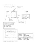
Table A–4 High–Speed Counters HSC0, HSC3, HSC4, and HSC5
Mode HSC0 HSC3 HSC4 HSC5
I0.0 I0.1 I0.2 I0.1 I0.3 I0.4 I0.5 I0.4
0 Clk Clk Clk Clk
1 Clk Reset Clk Reset
2
3 Clk Direction Clk Direction
4 Clk Direction Reset Clk Direction Reset
5
6 Clk Up Clk Down Clk Up Clk Down
7 Clk Up Clk Down Reset Clk Up Clk Down Reset
8
9 Phase A Phase B Phase A Phase B
10 Phase A Phase B Reset Phase A Phase B Reset
11
Table A–5 High–Speed Counters HSC1 and HSC2
Mode HSC1 HSC2
I0.6 I0.7 I1.0 I1.1 I1.2 I1.3 I1.4 I1.5
0 Clk Clk
1 Clk Reset Clk Reset
2 Clk Reset Start Clk Reset Start
3 Clk Direction Clk Direction
4 Clk Direction Reset Clk Direction Reset
5 Clk Direction Reset Start Clk Direction Reset Start
6 Clk Up Clk Down Clk Up Clk Down
7 Clk Up Clk Down Reset Clk Up Clk Down Reset
8 Clk Up Clk Down Reset Start Clk Up Clk Down Reset Start
9 Phase A Phase B Phase A Phase B
10 Phase A Phase B Reset Phase A Phase B Reset
11 Phase A Phase B Reset Start Phase A Phase B Reset Start
4
Boolean Instructions
LD Bit
LDI Bit
LDN Bit
LDNI Bit
Load
Load Immediate
Load Not
Load Not Immediate
A Bit
AI Bit
AN Bit
ANI Bit
AND
AND Immediate
AND Not
AND Not Immediate
O Bit
OI Bit
ON Bit
ONI Bit
OR
OR Immediate
OR Not
OR Not Immediate
LDBx IN1, IN2 Load result of Byte Compare
IN1 (x:<, <=,=, >=, >, <>I) IN2
ABx IN1, IN2 AND result of Byte Compare
IN1 (x:<, <=,=, >=, >, <>) IN2
OBx IN1, IN2 OR result of Byte Compare
IN1 (x:<, <=,=, >=, >, <>) IN2
LDWx IN1, IN2 Load result of Word Compare
IN1 (x:<, <=,=, >=, >, <>) IN2
AWx IN1, IN2 AND result of Word Compare
IN1 (x:<, <=,=, >=, >, <>)I N2
OWx IN1, IN2 OR result of Word Compare
IN1 (x:<, <=,=, >=, >, <>) IN2
LDDx IN1, IN2 Load result of DWord Compare
IN1 (x:<, <=,=, >=, >, <>) IN2
ADx IN1, IN2 AND result of DWord Compare
IN1 (x:<, <=,=, >=, >, <>)IN2
ODx IN1, IN2 OR result of DWord Compare
IN1 (x:<, <=,=, >=, >, <>) IN2
LDRx IN1, IN2 Load result of Real Compare
IN1 (x:<, <=,=, >=, >, <>) IN2
ARx IN1, IN2 AND result of Real Compare
IN1 (x:<, <=,=, >=, >, <>) IN2
ORx IN1, IN2 OR result of Real Compare
IN1 (x:<, <=,=, >=, >, <>) IN2
NOT Stack Negation
EU
ED
Detection of Rising Edge
Detection of Falling Edge
= Bit
=I Bit
Assign Value
Assign Value Immediate
S Bit, N
R Bit, N
SI Bit, N
RI Bit, N
Set bit Range
Reset bit Range
Set bit Range Immediate
Reset bit Range Immediate
LDSx IN1, IN2
ASx IN1, IN2
OSx IN1, IN2
Load result of String Compare
IN1 (x: =, <>) IN2
AND result of String Compare
IN1 (x: =, <>) IN2
OR result of String Compare
IN1 (x: =, <>) IN2
ALD
OLD
And Load
Or Load
LPS
LRD
LPP
LDS N
Logic Push (stack control)
Logic Read (stack control)
Logic Pop (stack control)
Load Stack (stack control)
AENO And ENO
Math, Increment, and Decrement instructions
+I IN1, OUT
+D IN1, OUT
+R IN1, OUT
Add Integer, Double Integer or Real
IN1+OUT=OUT
-I IN1, OUT
-D IN1, OUT
-R IN1, OUT
Subtract Integer, Double Integer, or
Real
OUT-IN1=OUT
MUL IN1, OUT Multiply Integer (16*16->32)
*I IN1, OUT
*D IN1, OUT
*R IN1, IN2
Multiply Integer, Double Integer, or
Real
IN1 * OUT = OUT
DIV IN1, OUT Divide Integer (16/16->32)
/I IN1, OUT
/D, IN1, OUT
/R IN1, OUT
Divide Integer, Double Integer, or
Real
OUT / IN1 = OUT
SQRT IN, OUT Square Root
LN IN, OUT Natural Logarithm
EXP IN, OUT Natural Exponential
SIN IN, OUT Sine
COS IN, OUT Cosine
TAN IN, OUT Tangent
INCB OUT
INCW OUT
INCD OUT
Increment Byte, Word or DWord
DECB OUT
DECW OUT
DECD OUT
Decrement Byte, Word, or DWord
PID TBL, LOOP PID Loop
Timer and Counter Instructions
TON Txxx, PT
TOF Txxx, PT
TONR Txxx, PT
On–Delay Timer
Off–Delay Timer
Retentive On–Delay Timer
CTU Cxxx, PV
CTD Cxxx, PV
CTUD Cxxx, PV
Count Up
Count Down
Count Up/Down
Real Time Clock Instructions
TODR T
TODW T
Read Time of Day clock
Write Time of Day clock
Program Control Instructions
END Conditional End of Program
STOP Transition to STOP Mode
WDR WatchDog Reset (300 ms)
JMP N
LBL N
Jump to defined Label
Define a Label to Jump to
CALL N [N1,...]
CRET
Call a Subroutine [N1, ... up to 16
optional parameters]
Conditional Return from SBR
FOR INDX,INIT,FINAL
NEXT
For/Next Loop
LSCR N
SCRT N
CSCRE
SCRE
Load, Transition, Conditional End, and
End Sequence Control Relay
Move, Shift, and Rotate Instructions
MOVB IN, OUT
MOVW IN, OUT
MOVD IN, OUT
MOVR IN, OUT
Move Byte, Word, DWord, Real
BIR IN, OUT
BIW IN, OUT
Move Byte Immediate Read
Move Byte Immediate Write
BMB IN, OUT, N
BMW IN, OUT, N
BMD IN, OUT, N
Block Move Byte, Word, DWord
SWAP IN Swap Bytes