DSpace at VNU: STUDY OF MICROSTRUCTURE AND OPTICAL PROPERTIES OF PVA-CAPPED ZnS : Cu NANOCRYSTALLINE THIN FILMS
Bạn đang xem bản rút gọn của tài liệu. Xem và tải ngay bản đầy đủ của tài liệu tại đây (767.77 KB, 9 trang )
August
7,
S021886351000525X
2010 9:5 WSPC/S0218-8635
145-JNOPM
Journal of Nonlinear Optical Physics & Materials
Vol. 19, No. 2 (2010) 237–245
c World Scientific Publishing Company
DOI: 10.1142/S021886351000525X
J. Nonlinear Optic. Phys. Mat. 2010.19:237-245. Downloaded from www.worldscientific.com
by UNIVERSITY OF NEW ENGLAND LIBRARIES on 01/17/15. For personal use only.
STUDY OF MICROSTRUCTURE AND OPTICAL
PROPERTIES OF PVA-CAPPED ZnS : Cu
NANOCRYSTALLINE THIN FILMS
TRAN MINH THI∗,‡ , BUI HONG VAN† and PHAM VAN BEN†
∗Faculty
of Physics, Hanoi National University of Education,
136 Xuan Thuy, Cau Giay District, Hanoi, Vietnam
†Faculty
of Physics, College of Science, Hanoi National University,
334 Nguyen Trai, Hanoi, Vietnam
‡
Received 19 May 2010
A study has been carried out on the Cu doping and PVA capping induced optical
property changes in ZnS : Cu nanocrystalline powders and thin film. For this study,
ZnS : Cu nanopowders with Cu concentrations of 0.1%, 0.15%, 0.2%, 0.3% and 0.4%
are synthesized by the wet chemical method. The polyvinyl alcohol (PVA)-capped ZnS
thin film with 0.2% Cu concentration and various PVA concentrations are prepared
by the spin-coating method. The microstructures of the samples are investigated by
the X-ray diffraction (XRD) patterns and transmission electron microscopy (TEM).
The results show that the prepared samples belong to the wurtzite structure with the
average particle size of about 3–7 nm. The optical properties of samples are studied
by measuring absorption and photoluminescence (PL) spectra in the wavelength range
from 300 nm to 900 nm at 300 K. It is shown that the luminescent intensity of ZnS : Cu
nanopowders reaches the highest intensity for optimal Cu concentration of 0.2% with
the corresponding values of its direct band gap estimated to be about 3.90 eV. While the
PVA coating does not affect the microstructure of ZnS nanometerials, the PL spectra of
the samples are found to be affected by the PVA concentration as well as the exciting
power density. The influence of the polymer coating on the optical properties can be
explained by the quantum confinement effect of ZnS nanoparticles in the PVA matrix.
Keywords: PVA-capped ZnS : Cu nanocrystalline thin film; photoluminescence spectra;
absorption spectra.
1. Introduction
The ZnS nanomaterials are semiconducting material with direct and large band
gap. The direct band gap of ZnS is 3.60 eV for bulk ZnS material and 3.98 eV
for ZnS nanomaterial at 300 K1 in the wurzite structure. The direct band gap of
nanomaterials may be controlled by doping, polymer coating and changing the
preparation condition.2–5 The partial substitution of Zn by Cu was shown to have
considerable influence on the optical properties of the samples.9 Besides, the polymer coating used to protect ZnS nanoparticles from the environment influences
237
August
7,
S021886351000525X
J. Nonlinear Optic. Phys. Mat. 2010.19:237-245. Downloaded from www.worldscientific.com
by UNIVERSITY OF NEW ENGLAND LIBRARIES on 01/17/15. For personal use only.
238
2010 9:5 WSPC/S0218-8635
145-JNOPM
T. M. Thi, B. H. Van & P. V. Ben
is also expected to affect the optical properties of ZnS nanoparticles considerably
when the particles diffuse into the polymer matrix at a certain concentration. The
resulting changes are related to the quantum confinement or the quantum size effect
and the surface effect induced in the polymer-capped nanoparticles.1,6 The PVA
(polyvinyl alcohol) capped ZnS nanoparticle composites are applicable for a variety
of applications such as electro-luminescent devices, solar energy, and many other
optoelectronic devices.1,6,9 Recently, some authors have investigated the effects of
PVA1 and PVP6 (polyvinyl pyrrolidone) capping polymers of ZnS nanopowder and
thin films on the resulted optical properties of those samples.
In this paper, we present the research results on the role of Cu doping and
PVA-capping of ZnS nanoparticles and thin films. We studied firstly the variations
of optical properties of the ZnS : Cu nanopowder doped with various Cu concentrations of 0.1%, 0.15%, 0.2%, 0.3% and 0.4% (denoted by P1 , P2 , P3 , P4 , P5 ) which
allow us to determine the optimal concentration of Cu giving rise to the maximum
PL intensity in the visible spectral range. Secondly, we also study the influence of
the concentration of PVA (polyvinyl alcohol) capping polymer on the optical properties of the PVA capped ZnS : Cu nanopowder and the PVA coated nanocrystalline
thin films doped with the optimal Cu concentration. Furthermore, the influences
of Cu dopant and PVA concentration on the general features of the PL spectra, as
well as the optical band gap variation are also discussed.
2. Experimental Details
The ZnS : Cu nanopowder was prepared by the standard wet chemical method from
three separately prepared highly pure initial solutions. The first solution was the
Zn(CH3 COO)2 ·2H2 O of 0.1 M, the second solution was the Cu(CH3 COO)2 ·H2 O of
0.1 M and the third solution was the Na2 S·9H2 O of 0.1 M. The catalyst CH3 OH :
H2 O was used for first and second solutions in 1:1 volume ratio. The first solution
and the second solution were mixed with appropriate ratio in order to produce the
P1 , P2 , P3 , P4 , P5 powder samples. The water was the solvent used for the third
solution. The third solution was prepared with different amounts (1g, 2g, 3g and 4g)
of PVA, then added drop by drop into the reaction vessel containing the initially
mixed solution of 100 ml. The ZnS : Cu precipitates were separated by centrifuge at
spinning speed of about 3000 rpm and finally dried at 80◦ C. The reactions taking
place during the final mixing process are described as follows:
Zn(CH3 COO)2 + Na2 S = ZnS ↓ + 2CH3 COONa,
Cu(CH3 COO)2 + Na2 S = CuS ↓ + 2CH3 COONa.
These powder samples were designated by P-ZnS : Cu, P-ZnS : Cu-PVA1, P-ZnS :
Cu-PVA2, P-ZnS : Cu-PVA3, P-ZnS : Cu-PVA4 (with P standing for the powder
samples), corresponding to the optimally Cu doped ZnS:Cu nanopowder samples
with different concentrations of PVA capping material. Additionally, the PVAcoated Cu doped ZnS thin films were produced by spin-coating the final mixed
August
7,
S021886351000525X
2010 9:5 WSPC/S0218-8635
145-JNOPM
239
solution on the glass substrates. These films were denoted by F-ZnS : Cu-PVA1,
F-ZnS : Cu-PVA2, F-ZnS : Cu-PVA3 and F-ZnS : Cu-PVA4, respectively (with F
standing for film samples).
PL spectra of all the samples were firstly measured at 300 K by the fluorescence
spectrophotometer HP340–LP370 using a He-Cd laser source with the excitation
wavelength of 325 nm. The optimal dopant concentration giving rise to maximum
emission intensity was determined on the basis of this observation. The nanopowder
with this particular Cu dopant concentration as well as its PVA-capped samples
were to become the focus of the ensuing measurements. The microstructure of
these samples were investigated by X-ray diffraction patterns by means of the XD8
A. The partiAdvance Bukerding machine using the Cu-Kα radiation of λ = 1.5406 ˚
cle size was measured by means of transmission electron microscope TEM-HITACHI
H6000. The ultraviolet absorption spectra of the thin film samples were measured
by spectrophotometer JASCO-V670 . The dependence of the photoluminescence
spectra on the exciting laser power density was also investigated.
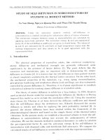
3. Results and Discussion
Figure 1 shows the PL spectra of P1, P2 , P3 , P4 , P5 powder samples, where the PL
peaks are found at practically the same wavelength of about 500 nm and do not
appear to be effected by the Cu-doped concentration. But the PL peak intensity
exhibits perceptible and non-monotonous changes with increasing Cu concentration.
It is seen from the figure that the maximum peak intensity comes from the sample
with the optimal Cu concentration of about 0.2%. We shall henceforth focus our
presentation and discussion on the measurement results of the optimally Cu-doped
samples (P-ZnS : Cu) of PVA-capped nanopowder and thin films.
Figure 2 shows the XRD patterns of P-ZnS : Cu, P-ZnS : Cu-PVA2 and P-ZnS :
Cu-PVA4 powders. The XRD patterns of the uncapped powder and the powder samples with PVA capping at different concentrations show that the crystal
Intensity (a.u.)
J. Nonlinear Optic. Phys. Mat. 2010.19:237-245. Downloaded from www.worldscientific.com
by UNIVERSITY OF NEW ENGLAND LIBRARIES on 01/17/15. For personal use only.
Study of Microstructure and Optical Properties of PVA-Capped
50000
45000
40000
35000
30000
25000
20000
15000
10000
5000
0
-5000
300
500 nm
P2
P4
P3
P5
P1
400
500
600
700
800
900
Wavelength (nm)
Fig. 1. The PL spectra of the P1 , P2 , P3 , P4 and P5 ZnS : Cu nano powder samples with the
0.1%, 0.15%, 0.2%, 0.3%, 0.4% Cu-doped concentrations, respectively.
August
7,
S021886351000525X
240
2010 9:5 WSPC/S0218-8635
145-JNOPM
T. M. Thi, B. H. Van & P. V. Ben
1000
a.P-ZnS:Cu
b.P-ZnS:Cu-PVA2
c. P-ZnS:Cu-PVA4
900
J. Nonlinear Optic. Phys. Mat. 2010.19:237-245. Downloaded from www.worldscientific.com
by UNIVERSITY OF NEW ENGLAND LIBRARIES on 01/17/15. For personal use only.
Intensity (a.u.)
800
(1 1 1)
700
(2 2 0)
600
(3 1 1)
500
400
c
300
a
200
b
100
20
Fig. 2.
30
40
50
2 theta
60
70
The XRD spectra of P-ZnS : Cu, P-ZnS : Cu-PVA2 and P-ZnS : Cu-PVA4 powder sample.
structure of the ZnS : Cu nanomaterials is of the wurtzite phase with the diffraction
peaks (1 1 1), (2 2 0), (3 1 1) in agreement with the previously reported result.1 It
is also to be noted that the PVA capping does not affect the crystal structure of
the ZnS : Cu nanomaterials. The average diameter of grains as calculated by the
Scherrer formular varies between 2.70 nm and 2.90 nm for uncapped powder, while
it is about 3.20 nm for the powder capped by PVA of highest concentration P-ZnS :
Cu-PVA4.
The morphology of the F-ZnS : Cu-PVA2 thin film was observed by TEM image
which is presented in Fig. 3. One observes the grain in sphere form were embedded
Fig. 3.
TEM image of F-ZnS : Cu-PVA2 thin film.
August
7,
S021886351000525X
2010 9:5 WSPC/S0218-8635
145-JNOPM
Study of Microstructure and Optical Properties of PVA-Capped
2.5
Absorption (a.u.)
a
2.0 c
a.
b.
c.
d.
241
F-ZnS:Cu-PVA1
F-ZnS:Cu-PVA2
F-ZnS:Cu-PVA3
F-ZnS:Cu-PVA4
d
1.5
b
1.0
0.5
300 350 400 450 500 550 600
J. Nonlinear Optic. Phys. Mat. 2010.19:237-245. Downloaded from www.worldscientific.com
by UNIVERSITY OF NEW ENGLAND LIBRARIES on 01/17/15. For personal use only.
Wavelength (nm)
Fig. 4.
The absorption spectra of the thin films with different PVA concentrations.
in the PVA matrix. The average size of the grain is about 3 nm which is in agreement
with the above calculated results from the XRD data which is slightly larger than
the particle sizes in the uncapped samples.
Figure 4 presents the absorption spectra of the F-ZnS : Cu-PVA1, F-ZnS : CuPVA2, F-ZnS : Cu-PVA3 and F-ZnS : Cu-PVA4 thin films. The relation between
the absorption coefficient α and the exciting photon energy can be calculated by
the following equation1,6 :
1
K(hν − Eg ) /2
.
(1)
hν
Here, K is a constant depending on the effective mass of the hole, the electron
and refractive index, and h is the Planck constant, ν the exciting photon frequency
and Eg the direct band gap. From Eq. (1) and the absorption spectra in Fig. 4,
the direct band gap can be calculated yielding the values of about 3.90 eV, 3.86 eV,
3.77 eV and 3.73 eV for the F-ZnS : Cu-PVA1, F-ZnS : Cu-PVA2, F-ZnS : Cu-PVA3
and F-ZnS : Cu-PVA4 thin films, respectively. Apparently, these Eg values are all
larger than that of the bulk ZnS (3.60 eV). One can further deduce the crystallite
radius r according to the following formula1 :
α=
∆Eg = Eg (film) − Eg (bulk) =
1
h2
1
1.8e2
.
+
−
8r2 m∗e
m∗h
εr
(2)
Here, Eg (bulk) is the band gap energy of the bulk sample, ε = 8.76, m∗e = 0.34 m0 ,
m∗h = 0.24 m0 , where m0 is the mass of the free electron. The calculated results of
crystallite radius r in these thin films are given in Table 1 along with the corresponding values of Eg . The results show that Eg decreases while the crystallite size
increases with increasing PVA concentration. The table also shows that F-ZnS : CuPVA1 thin film has the largest band gap and smallest grain size with Eg = 3.90 eV
and r = 3.60 nm.
The PL spectra of the thin films with different PVA concentration are presented
in Fig. 5. These spectra include the blue luminescence band at the left shoulder of
spectra and the green luminescence band at about 500 nm wavelength. It is clear
that the positions of luminescence peak remains more or less unchanged at about
August
7,
S021886351000525X
242
2010 9:5 WSPC/S0218-8635
145-JNOPM
T. M. Thi, B. H. Van & P. V. Ben
Table 1. The direct energy gaps and the radii r of the
nanocrystallites in the thin films.
Thin films
F-ZnS
F-ZnS
F-ZnS
F-ZnS
:
:
:
:
Intensity (a.u.)
r (nm)
3.90
3.86
3.77
3.73
3.60
4.20
5.60
7.50
Cu-PVA1
Cu-PVA2
Cu-PVA3
Cu-PVA4
a. F-ZnS : Cu-PVA1
b. F-ZnS : Cu-PVA2
c. F-ZnS : Cu-PVA3
d. F-ZnS : Cu-PVA4
e. F-ZnS : Cu
500 nm
30000
J. Nonlinear Optic. Phys. Mat. 2010.19:237-245. Downloaded from www.worldscientific.com
by UNIVERSITY OF NEW ENGLAND LIBRARIES on 01/17/15. For personal use only.
Eg (eV)
25000
20000
b
e
15000
10000
a
c
5000
d
0
300
400
500
600
700
800
900
1000
Wavelength (nm)
Fig. 5.
The PL spectra of the thin films with different PVA concentrations.
500 nm, implying that it was not effected by PVA concentration. However, the intensity of luminescence peak changes non-monotonously with the PVA concentration,
with the F-ZnS : Cu-PVA1, F-ZnS : Cu-PVA2 samples showing equally highest PL
intensities.
We further investigated the dependence of PL spectra on the exciting power
density. Figure 6 presents the PL spectra of the F-ZnS : Cu-PVA1 thin film
attained with the exciting wavelength of 325 nm and different exciting power densities. As expected, the luminescence peak position is observed to remain practically
unchanged when the power density varies from 0.20 W/cm2 to 0.45 W/cm2 . But
the associated intensity does change perceptibly and monotonously. It was found
that the variation of the peak intensity can be well-fitted by the power law of the
form IP L = A(IEX )n with n = 0.8. This result shows that the Cu is the emission
center of the luminescence band at around 500 nm.10
In addition, we compare the shift of PL peak of thin film sample with the ZnS :
Cu powder, prepared by solid-state reaction method with the same Cu dopant
but without PVA capping. The average diameter of the grain of this sample is
about 8µm. As presented in the Fig. 7, the luminescence peak of the thin film
sample is shifted towards shorter wavelength with respect to the luminescence peak
of the powder sample. This wavelength is observed to be shifted downwards by
about 30 nm, which corresponds to an energy of 140 meV. Meanwhile, the blue
August
7,
S021886351000525X
2010 9:5 WSPC/S0218-8635
145-JNOPM
Study of Microstructure and Optical Properties of PVA-Capped
1600
1400
1200
1000
800
600
400
200
J. Nonlinear Optic. Phys. Mat. 2010.19:237-245. Downloaded from www.worldscientific.com
by UNIVERSITY OF NEW ENGLAND LIBRARIES on 01/17/15. For personal use only.
0
300
400
500
600
700
800
243
August
7,
S021886351000525X
244
2010 9:5 WSPC/S0218-8635
145-JNOPM
T. M. Thi, B. H. Van & P. V. Ben
This change is explained as follows. It is known that the Bohr exciton radius
can be determined approximately by the following formula:
J. Nonlinear Optic. Phys. Mat. 2010.19:237-245. Downloaded from www.worldscientific.com
by UNIVERSITY OF NEW ENGLAND LIBRARIES on 01/17/15. For personal use only.
rB =
h2 ε 1
1
+ ∗ ,
πe2 m∗e
mh
(3)
with the dielectric constant ε = 8.76 for the material. The Bohr radius found by this
formula is about 2.5 nm. Since the size of the nanoparticles becomes comparable to
the Bohr-excitonic radius, the properties of nanocrystalline materials is expected to
change significantly as a result of quantum size effects, namely the band gap energy
increases with decreasing particle size. On the other hand, formula (2) shows that
the shift of the band gap energy is caused by the shift of the conduction band
to higher energy and the shift of the valence band to lower energy. However, the
energy shift of the conduction band is larger than the energy shift of the valence
band because the effective mass of the hole is smaller than the effective mass of the
electron in ZnS : Cu.
4. Conclusion
We produced successfully the ZnS : Cu nanopowders with different Cu concentrations and the F-ZnS : Cu-PVA1, F-ZnS : Cu-PVA2, F-ZnS : Cu-PVA3 and F-ZnS :
Cu-PVA4 thin films with the 0.2% optimal Cu dopant and different amounts of
PVA capping by the wet chemical method and the spin-coating method on glass
substrate. While the crystalline structure appears unaffected by the PVA, perceptible changes were observed in the grain size and optical energy gaps as well as the
PL intensity. It was also observed that the nanocrystallites became embedded in
the PVA matrix leading to reduced grain size and thereby induced the quantum
size effect which may explain the above-mentioned changes.
Acknowledgments
All authors of this paper would like to thank the organizing committee of ISMOA
2009. The paper is completed by the support of the Ministerial-level project on
the topic synthesized and optical properties of the 3d transition metal doped
ZnS/polymer composite materials, code B2010-17-234.
References
1. P. K. Ghosh, S. Jana, S. Nandy and K. K. Chattopadhyay, Materials Research Bulletin
42 (2007) 505–514.
2. A. A. Bol, J. Ferwerda, J. A. Bergweff and A. Meijerink, J. Luminescence 99 (2000)
325–334.
3. A. Ishizumi, C. W. White and Y. Kanemitsu, Appl. Phys. Lett. 84 (2004) 2397–2399.
4. M. Wang, K. Sun, X. Fu and C. L. C. Yan, Solid State Comm. 115 (2000) 492–496.
5. S. Lee, D. Song, D. Kim, J. Lee, S. Kim, I. Y. Park and Y. D. Choi, Materials Lett.
58(3–4) (2004) 342–346.
August
7,
S021886351000525X
2010 9:5 WSPC/S0218-8635
145-JNOPM
Study of Microstructure and Optical Properties of PVA-Capped
245
J. Nonlinear Optic. Phys. Mat. 2010.19:237-245. Downloaded from www.worldscientific.com
by UNIVERSITY OF NEW ENGLAND LIBRARIES on 01/17/15. For personal use only.
6. R. Maity, U. N. Maiti, M. K. Mitra and K. K. Chattopadhyay, Physica E 33 (2006)
104–09.
7. K. Jayanthi, S. Chawla, H. Chander and D. Haranath, Cryst. Res. Technol. 42(10)
(2007) 976–982.
8. P. Yang, M. Lu, D. Xu, D. Yuan and G. Zhou, Chem. Phy. Lett. 336 (2001) 76–80.
9. M. Oztas, M. Bedin, A. N. Yazici, E. V. Kafadar and H. Toktamis, Physica B 381
(2006) 40–46.
10. W. Chen, A. G. Joly, J.-O. Malm and J.-O. Bovin, J. Appl. Phys. 95(2) (2004) 667–
672.