DSpace at VNU: Fabrication and characterization of large-pixel size OLEDs used for opto-biomedical analysis
Bạn đang xem bản rút gọn của tài liệu. Xem và tải ngay bản đầy đủ của tài liệu tại đây (506.14 KB, 4 trang )
2012 International Conference on Biomedical Engineering and Biotechnology
Fabrication and Characterization of Large-Pixel Size
OLEDs Used For Opto-Biomedical Analysis
Nguyen Nang Dinh*, Nguyen Duc Cuong, Tran Thi
Thao, Do Ngoc Chung, Le Thi Hien
Tran Quang Trung
University of Natural Science, Vietnam National
University, Ho Chi Minh City
Ho Chi Minh City, Vietnam
University of Engineering and Technology,
Vietnam National University, Hanoi (UET-VNU)
Hanoi, Vietnam
Vu Xuan Nghia, Pham Duc Minh
Biomedical & Pharmaceutical Applied Research Center,
Vietnam Military Medical University
Hanoi, Vietnam
*) Corresponding author, Email:
in the emitting layer (EML) and (iii) radiative decay of
excitons. Recently, novel approaches to deal with these
problems have been reported [5, 6] such as the addition
of a hole transport layer (HTL) between the transparent
anode and the emitting layer (EML) [5] and/or of an
electron transport layer (ETL) sandwiched between the
EML and cathode [6].
With the aim to use a “flat film-like shape” excitation
Abstract—
source in the opto-biomedical analysis system (OBMAS), a
deep-blue organic light emitting diodes (OLED) with 240 mm2
in size and an emission wavelength of 455 nm were fabricated
by vacuum evaporation of low-molecular-weight polymers. In
the devices N, N-Bis(naphthalen-1-yl)-. N,N-bis(phenyl)
benzidine (NPB) was used for hole transport layer (HTL), 2methyl-9,10-bis(naphthalene-2-yl)anthracene (MADN) – for
emitting
layer
(EML)
and
tris(8hydroxyquinolinato)aluminum(III) (Alq3) – for electron
transport layer (ETL). The output power, the luminous
efficiency, the peak wavelength and the full width at halfmaximum (FWHM) of the deep-blue OLED were 1.5 mW, 1.0
cd/A, 455 nm and 100 nm, respectively, at a forward current of
30 mA. Under excitation of this excitation source, the
photoluminance of the CdSe-QDs attached with listeria
monocytogenes bacteria exhibit clear orange colour light. The
image of the luminance was detected by a 1.3 Mpx sensitive
webcam. This can be used in the biomedical analysis by using
an optic microscope acting like an opto-biomedical
microanalysis system (OBMAS). With use of the OBMAS one
can qualitatively detect the presence of bacteria attached to the
QDs through specific antibodies.
However, the efficiency of the devices as well as the
long-lasting service is sometimes limited because of the
large thickness of the laminar devices. So that the
thickness of each layer should be controlled as thin as
possible. But this results in a big difficulty in fabrication
of the OLEDs with a large area of emission, the problem
is how to avoid the pores and defects formed during the
preparation process, for the thin organic films in
particular.
As an excitation light, OLED possess another
advantage in comparison with LEDs in the flat film-like
shape that makes OLED easy to integrate monolithically
with microfluidic mixers made on flat glass substrates.
Kopelman et al [7] reported a fluorescent chemical
sensor platform integrating an OLED device light-source
with a fluorescent probe for oxygen sensor. Qiu and coworkers [8] presented an integrated PDMS microfluidic
device with a 520 nm (peak wavelength) green OLED
and optical fibers. Kim et al [9] reported an advanced
and compact microchip coupled with a green OLED of
530 nm (peak wavelength) and a PIN photodiode for
fluorescence detection which achieving a detection limit
of 10-5 M Rhodamine 6G (10 PM) as reported. In a labon-a-chip (LOC) the cross-polarized technique is
needed, as it can distinguish excitation light from
emission light by polarization, even if the excitation and
signal light overlap in wavelength.
Keywords: OLED; electroluminescence, excitation source;
opto-biomedical analysis.
I. INTRODUCTION
During the last decade, organic light emitting diodes
(OLEDs) have been increasingly investigated due to their
potential applications in many scopes, such as
optoelectronics, screen for TV and cellular phones, etc [1-4].
The main advantage of OLED compared to inorganic LED is
a possibly large area of the emission, that is desired for
replacing LED in urban lighting. However, in order to
replace the light emitting diodes (LEDs) based on inorganic
semiconducting materials, it is necessary to improve both the
efficiency and time of service of the OLEDs. The efficiency
of the optoelectronic devices like OLEDs, is controlled by
three factors: (i) equalization of injection rates of positive
(hole) and negative (electron) charge carriers (ii)
recombination of the charge carriers to form singlet excitons
In this work we present recent results on the
preparation and characterization of the large-pixel size
OLEDs that can be served as the flat film-like shape
excitation sources in the LOC for the opto-biomedical
analysis. The working principle of the opto-biomedical
analysis system (OBMAS) has also been investigated.
This work was supported by the MOST of Vietnam through a Project on
Fundamental Scientific Research and Applications in period of 2011 –
2013. Project Code: 1/2010/HD-DTNCCBUD.
978-0-7695-4706-0/12 $26.00 © 2012 IEEE
DOI 10.1109/iCBEB.2012.219
806
II. EXPERIMENTAL
Conducting polymers or organic semiconducting
materials used in this work are the “low-molecular-weight”
polymers like tris(8-hydroxyquinolinato)aluminum(III) or N,
N-Bis(naphthalen-1-yl)-. N,N-bis(phenyl) benzidine. Thin
or/and ultrathin films of these polymers can be made by
sublimating (evaporating) in vacuum. The initial materials
used for the evaporation are the polymers purchased from
Sigma-Aldrich Ltd. The chemicals, their abbreviation and
function in devices are listed in Table 1. All the layers in
devices were made by evaporation in high vacuum, the
pressure in the vacuum chamber is of ~ 2.5u10-4 Pa.
The ultraviolet-visible absorption spectra were carriedout on a JASCO UV-VIS-NIR V570. Photoluminescence
(PL) and Electroluminescence (EL) spectra were measured,
respectively on a FL3-2 spectrophotometer and a “Darsa
Pro-5000 system” with use of “Keithley-2400” dc-source.
The luminance of the OLEDs was estimated by using a
source measure unit of “Keithley 236 SMU” as the dcsource and “Minolta CS-100A” as the luminance meter.
The luminous efficiency was determined as the ratio of the
luminance density (cd/m2) and corresponding current
density (A/m2).
For detecting the presence of any bacteria, the DNA of
the last was attached to CdSe-QDs in a liquid solution. A
normal optic microscope was used with adding two crosspolarizers and an OLED served as the flat excitation source,
instead of the illuminating lamp. The PL images of samples
were taken by a high resolution webcam.
TABLE 1. INITIAL POLYMERS USED FOR PREPARATION OF OLEDS
Name
Abbreviation
Function
N, N-Bis(naphthalen-1-yl)-. N,Nbis(phenyl) benzidine
NPB
HTL
2-methyl-9,10-bis(naphthalene-2yl)anthracene
MADN
EML
Tris (8-hydroxyquinolinato)
aluminum(III)
Alq3
ETL or EML
Bis(10-hydroxybenzo [h] quinolinato)beryllium
Bebq2
ETL
III. RESULTS AND DISCUSSION
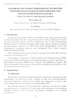
Comparing with Alq3 (C27H18AlN3O3), MADN (C35H24)
has a less complicated molecular structure (Fig. 1).
However, MADN is a prospective polymer that can be used
for the EML in OLEDs, because MADN is stable at
temperatures higher 330 oC and the sublimation efficiency is
larger 99%. Moreover, the bandgap of MADN is larger than
that of Alq3 [10].
The ITO-coated glass pieces with 25 mm u 25 mm in
size were used as substrates, further as the transparent anode.
The ITO coating was etched leaving a working area of 9
mm2, on each ITO piece there are four square cells. For the
large-area OLED, the working area consists of ~ 240 mm2
for one ITO piece. The substrates were ultrasonically
cleaned following three steps: 15 min in acetone, 10 min in
ethanol and 5 min in distilled water. Finally, the substrates
were dried by nitrogen gaseous flow and kept in a argon
glove-box until further use.
The organic layers NPB as HTL, MADN as EML and
Alq3 as ETL were obtained by deposition through shadow
mask in the high-vacuum chamber. Further, a shallow
contact (ultrathin LiF layer) with aluminum cathode (Al)
followed by 100 nm thick layer served as the cathode were
successively evaporated. The working area of OLED pixels
defined by the overlap of anode and cathode layouts is 3×3
mm2 (or 15×16 mm2 for the larger-area OLEDs). Finally,
the fabricated samples were hermetically encapsulated using
glass with getter before taking out of the glove-box for
measurements.
a.
b.
Figure 1. The molecular structure of Alq3 (a) and MADN (b)
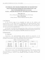
Figure 2 shows the absorption and photoluminescence
spectrum of the 1M MADN in dichloromethane. From this
figure one can see that MADN exhibits a peak at ~ 379 nm
in UV-VIS, in agreement with reported data in [10].
To characterize optospectroscopic properties (absorption
and photoluminescence) of the MADN, a solution of 1M
MADN in dichloromethane (MADN + DM) was prepared.
The thickness of the films was automatically controlled
by using a quart crystal microbalance (QCM) during
evaporation. For comparison, the different devices were
made, as follows (the number in brackets shows the
thickness of the films in nanometer):
ITO/NPB(50)/Alq3(40)/LiF(0.5)/Al
ITO/NPB(50)/Alq3(40)/Bebq2(20)/LiF(0.5)/Al
ITO/NPB(50)/Bebq2(40)/Alq3(20)/LiF(0.5)/Al
ITO/NPB(50)/MADN(50)/Alq3(20)/LiF(0.5)/Al
Figure 2. Absorption (a) and photoluminescence spectra (b) of the
MADN + DM solution. Excitation wavelength is O = 325 nm.
807
where J is a double charge injection factor which is
dependent on the processes of carrier injection and is
maximal (J = 1) if a balanced charge injection into the
emission layer of the device is achieved, i.e. the number of
injected negative charges (electrons) equals the number of
injected positive charges (holes); Kr quantifies the
efficiency of the formation of a singlet exciton from a
positive and a negative polaron, and If is the
photoluminescence quantum efficiency.
The absorption spectra of the MADN + DM solution is
broad, ranging from 350 to 450 nm. Under excitation of HeCd laser beam at O = 325 nm, the obtained PL spectrum
exhibits a peak at ~ 453 nm. One can expect that the MADN
used for the EML in OLEDs can emit a deep-blue colour,
when applying an appropriate potential onto the transparent
ITO anode. Indeed, from the EL spectra of three different
OLEDs in Fig. 3 one can see that for the MADN device, the
EL peak is observed at ~ 455 nm, this is quite consistent
with the wavelength of the PL peak.
Figure 4. The luminous efficiency vs. luminance of MADN device
without ETL (bottom curve) and with the ETL (top curve).
Figure 3. EL spectra of different laminar OLEDs:
The abrupt increase in efficiency occurred at the value
of luminance around 110 cd/m2. This relates to the most
effective current range corresponding polarized potentials
that was applied onto the transparent anode (ITO), where
the current density in the I-V characteristic raised with an
abrupt value.
“1” - ITO/NPB/Alq3/LiF/Al
“2” - ITO/NPB/Alq3/Bedq2/LiF/Al
“3” - ITO/NPB/MADN/LiF/Al
“4” - ITO/NPB/MADN/Alq3LiF/Al
In Fig. 3 there are presented also EL curves of two other
devices, the first is the OLED with using Alq3 served
simultaneously as EML and ETL, while the second one is
the OLED with using Alq3 and Bebq2 served as EML and
ETL, respectively. Although the addition of Bebq2 as the
ETL in OLED does not change the feature of the EL
spectrum, the luminance efficiency could be enhanced. The
Alq3 diode emits green colour at the EL peak at ~ 527 nm,
the full width of half maximum (FWHM) of the Alq3-OLED
is about 100 nm. The FWHM of the MADN-OLED is almost
the same value. The FWHM of the OLEDs is much larger
than that of inorganic LEDs, for instance the FWHM of
InGaN-LED is of 30 nm [11]. However, the large FWHM is
just an advantage of the OLED in using for the flat film-like
shape excitation source.
The deep-blue OLED with MADN as the EML was
used for a flat excitation source excitation in so called
“opto-biomedical microanalysis system” (OBMAS), which
is shown in Fig. 5. For testing the working principle of the
OBMAS, the colloidal CdSe quantum dots (CdSe-QDs)
with 18 – 20 nm in size were used, this material emits
luminance with a peak at ~ 655 nm [13-15]. CdSe-QDs
were attached with the DNA of some bacteria, for instance,
listeria monocytogenes bacteria (LMB). The deep-blue
light emitted from the OLED light was polarized by the
first polarizer to distinguish excitation light and signal light
(Fig. 5). The last emitted from the sample cell containing
colloidal CdSe-QDs attached with the LMB. The signal
light or luminous emission was recorded by using a
webcam with the resolution of 1.3 Mpx. The results on
observing the presence of the LMB are shown in Fig. 6.
The luminous efficiency vs. luminance of the devices is
plotted in Fig. 4. From this figure one can see that at the
same value of the luminance, the MADN-OLED with ETL
(Alq3) exhibits much larger luminance efficiency. The effect
of both the HTL and ETL on the enhancement of
electroluminescence efficiency or (luminance efficiency)
was well demonstrated, associated with the equalization
process of injection rates of holes and electrons. Indeed, The
electroluminescence efficiency can be determined by using
an expression obtained by Tsutsui and Saito in [12]:
KI
J uK r u I f
Without using polarizer 1, the image of the light emitted
from the deep-blue OLED is strongly bright (Fig. 6a) and
with using polarizer 1 and 2, the image became dark (Fig.
6b). This proves that the light was completely polarized by
polarize 1. When the sample cell was put on the pathway of
the polarized excitation light, we observed the luminance
image with the orange colour (Fig. 6c). The image reflects
the photoluminescence of the CdSe-QDs under excitation
of the deep-blue polarized light from the OLED. This
clearly shows that using OBMAS one can qualitatively
detect the presence of bacteria. However, to carry-out a fast
(1)
808
ACKNOWLEDGMENTS
One of us (T.T.T.) thanks Prof. N.N.Dinh for the
financial support during her M.Sc. study in UET-VNU.
bio-medical analysis, further we need to intergrate also a
microfluidic device to the OBMAS and to attach the bacteria
to the QDs through specific antibodies.
REFERENCES
[1]
[2]
[3]
[4]
[5]
Figure 5. Schema of an opto-biomedical analysis system based on an
optic microscope combined with two cross-polarizers and a photodigital
camera or a sensitive webcam.
[6]
[7]
[8]
a.
b.
c.
Figure 6. Image of the excitation beam without (a), with polarizer 1 (b)
and image of luminous emission of CdSe-QDs attached with LMB (c).
[9]
IV. CONCLUSIONS
Deep-blue OLEDs with 240 mm2 in size and an emission
wavelength of 455 nm were fabricated by vacuum
evaporation of low-molecular-weight polymers, such as NPB
for HTL, MADN – for EML and Alq3 – for ETL. The
emission spectrum possesses a full width of half maximum
(FWHM) of 100 nm. Using these OLEDs for a so called
“flat
film-like
shape”
excitation
source,
the
photoluminescence of the CdSe-QDs attached with listeria
monocytogenes bacteria exhibited clear orange colour light.
The image of the luminance was detected due to taking a
photograph by a sensitive webcam. This suggests a very
useful application for the biomedical analysis by using an
optic microscope incorporated with two cross-polarizers that
can work as an opto-biomedical microanalysis system
(OBMAS). With use of the OBMAS one can qualitatively
detect the presence of the bacteria, once the last are attached
to the QDs through specific antibodies.
[10]
[11]
[12]
[13]
[14]
[15]
809
J. S. Salafsky, “Exciton dissociation, charge transport, and
recombination in ultrathin, conjugated polymer-TiO2 nanocrystal
intermixed composites,” Phys. Rev. B vol. 59, pp. 10885–10894, 1999.
V. M. Burlakov, K. Kawata, H. E. Assender, G. A. D. Briggs, A.
Ruseckas, and I. D. W. Samuel, “Discrete hopping model of
exciton transport in disordered media,” Phys. Rev. B vol. 72, pp.
075206-1 ÷ 075206-5, 2005.
A. Petrella, M. Tamborra, P. D. Cozzoli, M. L. Curri, M.
Striccoli, P. Cosma, G. M. Farinola, F. Babudri, F. Naso, and A.
Agostiano, “TiO2 nanocrystals–MEH-PPV composite thin films
as photoactive material,” Thin Solid Films, vol. 451/452, pp.
64 – 68, 2004.
H. Spanggaard and F. C. Kerbs, “A brief history of the
development of organic and polymeric photovoltaics,” Sol.
Energy. Mat. Sol. Cells, vol. 83, pp. 125–146, 2004.
D. E. Markov and P. W. M. Blom, “Migration-assisted energy
transfer at conjugated polymer/metal interfaces,” Phys. Rev. B
vol. 72, pp. 161401(R)–161404(R), 2005.
K. Kawata, V. M. Burlakov, M. J. Carey, H. E. Assender, G. A.
D. Briggs, A. Ruseckas, and I. D. W. Samuel, “Description of
exciton transport in a TiO2/MEH, PPV heterojunction
photovoltaic material,” Sol. Energy Mat. Sol Cells vol. 87,
pp.715–724, 2005.
V. Savvate’ev, Z. Chen-Esterlit, J. W. Aylott, B. Choudhury, C.
H. Kim, L. Zou, J. H. Friedl, R. Shinar, J. Shinar, and R.
Kopelman,
“Integrated
organic
light-emitting
device/fluorescence-based chemical sensors,” Appl. Phys. Lett.,
vol. 81, pp. 4652–4557, 2002.
B. Yao, G. Luo, L. Wang, Y. Gao, G. Lei, K.Ren, L. Chen, Y.
Wang, Y. Hu, and Y. Qiu, “A microfluidic device using a green
organic light emitting diode as an integrated excitation source,”
Lab on a Chip, vol. 5, pp. 1041–1047, 2005.
J. H. Kim, K. S. Shin, K. K. Paek, Y. H. Kim, Y. M. Kim, Y. K.
Kim, T. S. Kim, J. Y. Kang, E. G. Yang, S. S. Kim, and B. K. Ju,
Proc. Micro TAS 2004 (8-th International Conference on
Miniaturized System for Chemistry and Life Science, eds. T.
Laurell, J. Nilsson, K. Jensen, D.J. Harrison and J.P. Kutter, The
Royal Society of Chemistry, Cambridge, UK, 2004, pp. 428–432.
Catalogue of “Lumtec”- Luminescence Technology Corp., OLED
materials, 2011.
S. Nakamura, M. Senoh, N. Iwasa, S. Nagahama, T. Yamada,
and T. Mukai, “Superbright Green InGaN Single-QuantumWell-Structure Light-Emitting Diodes,” Jpn. J. Appl. Phys. Vol.
34 pp. L1332–L1335, 1995.
T. Tsutsui and S. Saito, “Intrinsically conducting polymers: an
emerging technology,” Edited by M. Aldissi. NATO ASI Series
E: Applied Sciences, vol 246, pp.123–127, 1993.
M. J. Archer and J. L. Liu, “Bacteriophage T4 Nanoparticles as
Materials in Sensor Applications: Variables That Influence Their
Organization and Assembly on Surfaces,” Sensors, vol. 9(8) pp.
6298 – 6311, 2009.
N. K. Pettya, T. J. Evansa, P. C. Finerana, and G. P. C. Salmond,
“Bio- technological exploitation of bacteriophage research,”
Trends. Biotechnol., Vol. 25, pp. 7–15, 2006.
M. Manchester and P. Singh, “Virus-based nanoparticles
(VNPs): platform technologies for diagnostic imaging,” Adv
Drug Deliv Rev, vol. 58 (2006) 1505 – 1522, 2006.