Tiêu chuẩn IPC 2221a
Bạn đang xem bản rút gọn của tài liệu. Xem và tải ngay bản đầy đủ của tài liệu tại đây (1.37 MB, 124 trang )
ASSOCIATION CON N ECTIN G
ELECTRON ICS IN DUSTRIES ®
IPC-2221A
Generic Standard on
Printed Board Design
IPC-2221A
May 2003
Supersedes IPC-2221
February 1998
A standard developed by IPC
2 2 1 5 Sander s Road, Nor thbr ook, IL 6 0 0 6 2 -6 1 3 5
Tel. 8 4 7 .5 0 9 .9 7 0 0 Fax 8 4 7 .5 0 9 .9 7 9 8
www.ipc.or g
The Principles of
Standardization
In May 1995 the IPC’s Technical Activities Executive Committee adopted Principles of
Standardization as a guiding principle of IPC’s standardization efforts.
Standards Should:
• Show relationship to Design for Manufacturability
(DFM) and Design for the Environment (DFE)
• Minimize time to market
• Contain simple (simplified) language
• Just include spec information
• Focus on end product performance
• Include a feedback system on use and
problems for future improvement
Notice
Standards Should Not:
• Inhibit innovation
• Increase time-to-market
• Keep people out
• Increase cycle time
• Tell you how to make something
• Contain anything that cannot
be defended with data
IPC Standards and Publications are designed to serve the public interest through eliminating misunderstandings between manufacturers and purchasers, facilitating interchangeability and improvement of products, and assisting the purchaser in selecting and obtaining with minimum delay the
proper product for his particular need. Existence of such Standards and Publications shall not in
any respect preclude any member or nonmember of IPC from manufacturing or selling products
not conforming to such Standards and Publication, nor shall the existence of such Standards and
Publications preclude their voluntary use by those other than IPC members, whether the standard
is to be used either domestically or internationally.
Recommended Standards and Publications are adopted by IPC without regard to whether their adoption may involve patents on articles, materials, or processes. By such action, IPC does not assume
any liability to any patent owner, nor do they assume any obligation whatever to parties adopting
the Recommended Standard or Publication. Users are also wholly responsible for protecting themselves against all claims of liabilities for patent infringement.
IPC Position
Statement on
Specification
Revision Change
It is the position of IPC’s Technical Activities Executive Committee (TAEC) that the use and
implementation of IPC publications is voluntary and is part of a relationship entered into by
customer and supplier. When an IPC publication is updated and a new revision is published, it
is the opinion of the TAEC that the use of the new revision as part of an existing relationship
is not automatic unless required by the contract. The TAEC recommends the use of the latest
revision.
Adopted October 6. 1998
Why is there
a charge for
this document?
Your purchase of this document contributes to the ongoing development of new and updated industry standards and publications. Standards allow manufacturers, customers, and suppliers to understand one another better. Standards allow manufacturers greater efficiencies when they can set
up their processes to meet industry standards, allowing them to offer their customers lower costs.
IPC spends hundreds of thousands of dollars annually to support IPC’s volunteers in the standards
and publications development process. There are many rounds of drafts sent out for review and
the committees spend hundreds of hours in review and development. IPC’s staff attends and participates in committee activities, typesets and circulates document drafts, and follows all necessary
procedures to qualify for ANSI approval.
IPC’s membership dues have been kept low to allow as many companies as possible to participate.
Therefore, the standards and publications revenue is necessary to complement dues revenue. The
price schedule offers a 50% discount to IPC members. If your company buys IPC standards and
publications, why not take advantage of this and the many other benefits of IPC membership as
well? For more information on membership in IPC, please visit www.ipc.org or call 847/790-5372.
Thank you for your continued support.
©Copyright 2003. IPC, Northbrook, Illinois. All rights reserved under both international and Pan-American copyright conventions. Any copying,
scanning or other reproduction of these materials without the prior written consent of the copyright holder is strictly prohibited and constitutes
infringement under the Copyright Law of the United States.
IPC-2221A
A SSOCIATION CON N ECTIN G
EL ECTRON ICS IN D U STRIES ®
Generic Standard on
Printed Board Design
Developed by the IPC-2221 Task Group (D-31b) of the Rigid Printed
Board Committee (D-30) of IPC
Supersedes:
IPC-2221 - February 1998
Users of this publication are encouraged to participate in the
development of future revisions.
Contact:
IPC
2215 Sanders Road
Northbrook, Illinois
60062-6135
Tel 847 509.9700
Fax 847 509.9798
HIERARCHY OF IPC DESIGN SPECIFICATIONS
(2220 SERIES)
IPC-2221
GENERIC DESIGN
IPC-2222
RIGID
IPC-2223
FLEX
IPC-2224
PCMCIA
IPC-2225
MCM-L
IPC-2226
HDIS
FOREWORD
This standard is intended to provide information on the generic requirements for organic printed board design. All aspects
and details of the design requirements are addressed to the extent that they can be applied to the broad spectrum of those
designs that use organic materials or organic materials in combination with inorganic materials (metal, glass, ceramic, etc.)
to provide the structure for mounting and interconnecting electronic, electromechanical, and mechanical components. It is
crucial that a decision pertaining to the choice of product types be made as early as possible. Once a component mounting
and interconnecting technology has been selected the user should obtain the sectional document that provides the specific
focus on the chosen technology.
It may be more effective to consider alternative printed board construction types for the product being designed. As an
example the application of a rigid-flex printed wiring board may be more cost or performance effective than using multiple
printed wiring boards, connectors and cables.
IPC’s documentation strategy is to provide distinct documents that focus on specific aspect of electronic packaging issues.
In this regard document sets are used to provide the total information related to a particular electronic packaging topic. A
document set is identified by a four digit number that ends in zero (0).
Included in the set is the generic information which is contained in the first document of the set and identified by the four
digit set number. The generic standard is supplemented by one or many sectional documents each of which provide specific
focus on one aspect of the topic or the technology selected. The user needs, as a minimum, the generic design document,
the sectional of the chosen technology, and the engineering description of the final product.
As technology changes specific focus standards will be updated, or new focus standards added to the document set. The IPC
invites input on the effectiveness of the documentation and encourages user response through completion of ‘‘Suggestions
for Improvement’’ forms located at the end of each document.
May 2003
IPC-2221A
Acknowledgment
Any document involving a complex technology draws material from a vast number of sources. While the principal members
of the IPC-2221 Task Group (D-31b) of the Rigid Printed Board Committee (D-30) are shown below, it is not possible to
include all of those who assisted in the evolution of this Standard. To each of them, the members of the IPC extend their
gratitude.
Rigid Printed Board
Committee
IPC-2221 Task Group
Chair
C. Don Dupriest
Lockheed Martin Missiles
and Fire Control
Chair
Lionel Fullwood
WKK Distribution Ltd.
Technical Liaison of the
IPC Board of Directors
Nilesh S. Naik
Eagle Circuits Inc.
IPC-2221 Task Group
Lance A. Auer, Tyco Printed Circuit
Group
Stephen Bakke, C.I.D., Alliant
Techsystems Inc.
Frank Belisle, Hamilton Sundstrand
Mark Bentlage, IBM Corporation
Robert J. Black, Northrop Grumman
Corporation
Gerald Leslie Bogert, Bechtel Plant
Machinery, Inc.
John L. Bourque, C.I.D., Shure Inc.
Scott A. Bowles, Sovereign Circuits
Inc.
Ronald J. Brock, NSWC - Crane
Mark Buechner
Lewis Burnett, Honeywell Inc.
Byron Case, L-3 Communications
Ignatius Chong, Celestica
International Inc.
Christine R. Coapman, Delphi Delco
Electronics Systems
Christopher Conklin, Lockheed
Martin Corporation
David J. Corbett, Defense Supply
Center Columbus
Brian Crowley, Hewlett-Packard
Company
William C. Dieffenbacher, BAE
Systems Controls
Gerhard Diehl, Alcatel SEL AG
C. Don Dupriest, Lockheed Martin
Missiles and Fire Control
John Dusl, Lockheed Martin
Theodore Edwards, Dynaco Corp.
Werner Engelmaier, Engelmaier
Associates, L.C.
Gary M. Ferrari, C.I.D.+, Ferrari
Technical Services
George Franck, C.I.D.+, Raytheon
E-Systems
Mahendra S. Gandhi, Northrop
Grumman
Hue T. Green, Lockheed Martin
Space and Strategic Missiles
Ken Greene, Siemens Energy &
Automation
Michael R. Green, Lockheed Martin
Space and Strategic Missiles
Dr. Samy Hanna, AT&S Austria
Technologie & System
Richard P. Hartley, C.I.D., Hartley
Enterprises
William Hazen, Raytheon Company
Phillip E. Hinton, Hinton ’PWB’
Engineering
Michael Jouppi, Thermal Man, Inc.
Thomas E. Kemp Rockwell Collins
Frank N. Kimmey, C.I.D.+,
PowerWave Technologies, Inc.
Narinder Kumar, C.I.D., Solectron
Invotronics
Clifford H. Lamson, C.I.D.+, Plexus
Technology Group
Roger H. Landolt, Cookson
Electronics
Michael G. Luke, C.I.D., Raytheon
Company
Wesley R. Malewicz, Siemens
Medical Systems Inc.
Kenneth Manning, Raytheon
Company
Susan S. Mansilla, Robisan
Laboratory Inc.
Rene R. Martinez, Northrop
Grumman
Brian C. McCrory, Delsen Testing
Laboratories
Randy McNutt, Northrop Grumman
John H. Morton, C.I.D., Lockheed
Martin Corporation
Bob Neves, Microtek Laboratories
Benny Nilsson, Ericsson AB
Steven M. Nolan, C.I.D.+, Silicon
Graphics Computer System
Randy R. Reed, Merix Corporation
Kelly M. Schriver, Schriver
Consultants
Jeff Seekatz, Raytheon Company
Kenneth C. Selk, Northrop Grumman
Russell S. Shepherd, Microtek
Laboratories
Lowell Sherman, Defense Supply
Center Columbus
Akikazu Shibata, Ph.D., JPCA-Japan
Printed Circuit Association
Jeff Shubrooks, Raytheon Company
Mark Snow, BAE Systems
Roger Su, L-3 Communications
Ronald E. Thompson, NSWC - Crane
Max E. Thorson, C.I.D.,
Hewlett-Packard Company
Dung Q. Tiet, Lockheed Martin
Space and Strategic Missiles
Dewey Whittaker, Honeywell Inc.
David L. Wolf, Conductor Analysis
Technology, Inc.
James V. Yohe, C.I.D., Yohe Design
Services
iii
IPC-2221A
May 2003
Table of Contents
SCOPE ...................................................................... 1
4.1.1
Material Selection for Structural Strength ....... 17
1.1
Purpose ................................................................ 1
4.1.2
Material Selection for Electrical Properties .... 17
1.2
Documentation Hierarchy .................................. 1
4.1.3
1.3
Presentation ......................................................... 1
Material Selection for Environmental
Properties .......................................................... 17
1.4
Interpretation ....................................................... 1
4.2
1.5
Definition of Terms ............................................ 1
1.6
Classification of Products ................................... 1
4.2.1
Dielectric Base Materials (Including
Prepregs and Adhesives) .................................. 17
Preimpregnated Bonding Layer (Prepreg) ....... 17
1.6.1
Board Type ......................................................... 1
4.2.2
Adhesives .......................................................... 17
1.6.2
Performance Classes ........................................... 1
4.2.3
Adhesive Films or Sheets ................................ 19
1.6.3
Producibility Level ............................................. 2
4.2.4
Electrically Conductive Adhesives .................. 19
1.7
Revision Level Changes ..................................... 2
4.2.5
4.3
Thermally Conductive/Electrically
Insulating Adhesives ......................................... 19
Laminate Materials ........................................... 20
IPC ...................................................................... 2
4.3.1
Color Pigmentation ........................................... 20
2.2
Joint Industry Standards ..................................... 3
4.3.2
Dielectric Thickness/Spacing ........................... 20
2.3
Society of Automotive Engineers ...................... 3
4.4
Conductive Materials ........................................ 20
2.4
American Society for Testing and Materials ..... 3
4.4.1
Electroless Copper Plating ............................... 20
2.5
Underwriters Labs .............................................. 3
4.4.2
Semiconductive Coatings ................................. 20
2.6
IEEE .................................................................... 3
4.4.3
Electrolytic Copper Plating .............................. 20
2.7
ANSI ................................................................... 4
4.4.4
Gold Plating ...................................................... 20
1
2
2.1
APPLICABLE DOCUMENTS ................................... 2
4.4.5
Nickel Plating ................................................... 22
GENERAL REQUIREMENTS ................................... 4
4.4.6
Tin/Lead Plating ............................................... 22
3.1
Information Hierarchy ........................................ 6
4.4.7
Solder Coating .................................................. 22
3.1.1
Order of Precedence ........................................... 6
4.4.8
3.2
Design Layout .................................................... 6
Other Metallic Coatings for Edgeboard
Contacts ............................................................ 23
3.2.1
End-Product Requirements ................................. 6
4.4.9
Metallic Foil/Film ............................................. 23
3.2.2
Density Evaluation ............................................. 6
4.4.10
Electronic Component Materials ...................... 23
3.3
Schematic/Logic Diagram .................................. 6
4.5
Organic Protective Coatings ............................. 24
3.4
Parts List ............................................................. 6
4.5.1
Solder Resist (Solder Mask) Coatings ............. 24
3.5
Test Requirement Considerations ....................... 7
4.5.2
Conformal Coatings .......................................... 25
3.5.1
Printed Board Assembly Testability ................... 7
4.5.3
Tarnish Protective Coatings ............................. 25
3.5.2
Boundary Scan Testing ....................................... 8
4.6
Marking and Legends ....................................... 25
3.5.3
Functional Test Concern for Printed Board
Assemblies .......................................................... 8
4.6.1
ESD Considerations .......................................... 26
3.5.4
In-Circuit Test Concerns for Printed Board
Assemblies ........................................................ 10
3
Fabrication Considerations ............................... 26
5.1.1
Bare Board Fabrication .................................... 26
5.2
Product/Board Configuration ............................ 26
5.2.1
Board Type ....................................................... 26
5.2.2
Board Size ........................................................ 26
5.2.3
Board Geometries (Size and Shape) ................ 26
5.2.4
Bow and Twist .................................................. 27
5.2.5
Structural Strength ............................................ 27
MATERIALS ............................................................ 17
5.2.6
Composite (Constraining-Core) Boards ........... 27
Material Selection ............................................. 17
5.2.7
Vibration Design ............................................... 29
Mechanical ........................................................ 12
3.5.6
Electrical ........................................................... 12
3.6
Layout Evaluation ............................................ 13
3.6.1
Board Layout Design ....................................... 13
3.6.2
Feasibility Density Evaluation ......................... 13
3.7
Performance Requirements .............................. 15
4
iv
MECHANICAL/PHYSICAL PROPERTIES ............. 26
5.1
3.5.5
4.1
5
May 2003
IPC-2221A
5.3
Assembly Requirements ................................... 30
5.3.1
Mechanical Hardware Attachment ................... 30
5.3.2
Part Support ...................................................... 30
7.3
5.3.3
Assembly and Test ........................................... 30
7.3.1
5.4
Dimensioning Systems ..................................... 31
5.4.1
Dimensions and Tolerances .............................. 31
5.4.2
Component and Feature Location .................... 31
5.4.3
Datum Features ................................................. 31
6
ELECTRICAL PROPERTIES ................................. 37
6.1
Electrical Considerations .................................. 37
6.1.1
Electrical Performance ..................................... 37
6.1.2
Power Distribution Considerations .................. 37
6.1.3
Circuit Type Considerations ............................. 39
6.2
Conductive Material Requirements .................. 40
6.3
Electrical Clearance .......................................... 42
6.3.1
B1–Internal Conductors .................................... 42
6.3.2
B2–External Conductors, Uncoated, Sea
Level to 3050 m [10,007 feet] ......................... 42
B3–External Conductors, Uncoated, Over
3050 m [10,007 feet] ........................................ 42
6.3.3
6.3.4
6.3.5
6.3.6
B4–External Conductors, with Permanent
Polymer Coating (Any Elevation) ................... 42
A5–External Conductors, with Conformal
Coating Over Assembly (Any Elevation) ........ 43
A6–External Component Lead/Termination,
Uncoated, Sea Level to 3050 m
[10,007 feet] ..................................................... 43
7.2.4
Special Design Considerations for SMT
Board Heatsinks ................................................ 52
Heat Transfer Techniques ................................. 52
7.3.2
Coefficient of Thermal Expansion (CTE)
Characteristics ................................................... 52
Thermal Transfer .............................................. 53
7.3.3
Thermal Matching ............................................ 53
7.4
Thermal Design Reliability .............................. 53
8
COMPONENT AND ASSEMBLY ISSUES ............. 55
8.1
General Placement Requirements .................... 55
8.1.1
Automatic Assembly ........................................ 55
8.1.2
Component Placement ...................................... 55
8.1.3
Orientation ........................................................ 57
8.1.4
Accessibility ...................................................... 57
8.1.5
Design Envelope ............................................... 57
8.1.6
Component Body Centering ............................. 57
8.1.7
Mounting Over Conductive Areas ................... 57
8.1.8
Clearances ......................................................... 58
8.1.9
Physical Support ............................................... 58
8.1.10
Heat Dissipation ............................................... 59
8.1.11
Stress Relief ...................................................... 60
8.2
General Attachment Requirements .................. 60
8.2.1
Through-Hole .................................................... 60
8.2.2
Surface Mounting ............................................. 60
8.2.3
Mixed Assemblies ............................................ 61
8.2.4
Soldering Considerations .................................. 61
6.3.7
A7–External Component Lead/Termination,
with Conformal Coating (Any Elevation) ....... 43
8.2.5
Connectors and Interconnects .......................... 62
8.2.6
Fastening Hardware .......................................... 63
6.4
Impedance Controls .......................................... 43
8.2.7
Stiffeners ........................................................... 64
6.4.1
Microstrip .......................................................... 44
8.2.8
Lands for Flattened Round Leads .................... 64
6.4.2
Embedded Microstrip ....................................... 44
8.2.9
Solder Terminals ............................................... 64
6.4.3
Stripline Properties ........................................... 44
8.2.10
Eyelets ............................................................... 65
6.4.4
Asymmetric Stripline Properties ...................... 46
8.2.11
Special Wiring .................................................. 65
6.4.5
Capacitance Considerations .............................. 46
8.2.12
Heat Shrinkable Devices .................................. 67
6.4.6
Inductance Considerations ................................ 47
8.2.13
Bus Bar ............................................................. 67
8.2.14
Flexible Cable ................................................... 67
7
THERMAL MANAGEMENT .................................... 48
7.1
Cooling Mechanisms ........................................ 48
8.3
Through-Hole Requirements ............................ 67
7.1.1
Conduction ........................................................ 49
8.3.1
Leads Mounted in Through-Holes ................... 67
7.1.2
Radiation ........................................................... 49
8.4
Standard Surface Mount Requirements ........... 71
7.1.3
Convection ........................................................ 49
8.4.1
Surface-Mounted Leaded Components ............ 71
7.1.4
Altitude Effects ................................................. 49
8.4.2
Flat-Pack Components ...................................... 71
7.2
Heat Dissipation Considerations ...................... 49
8.4.3
Ribbon Lead Termination ................................. 72
7.2.1
Individual Component Heat Dissipation .......... 50
8.4.4
Round Lead Termination .................................. 72
7.2.2
Thermal Management Considerations for
Board Heatsinks ................................................ 50
8.4.5
Component Lead Sockets ................................. 72
8.5
Fine Pitch SMT (Peripherals) .......................... 72
Assembly of Heatsinks to Boards .................... 50
8.6
Bare Die ............................................................ 73
7.2.3
v
IPC-2221A
8.6.1
Wire Bond ......................................................... 73
8.6.2
Flip Chip ........................................................... 73
8.6.3
Chip Scale ......................................................... 73
8.7
Tape Automated Bonding ................................. 73
8.8
Solderball .......................................................... 73
May 2003
11.4.3
12
Solder Resist Coating Phototools .................... 83
QUALITY ASSURANCE ....................................... 83
12.1
Conformance Test Coupons ............................. 83
12.2
Material Quality Assurance .............................. 84
12.3
Conformance Evaluations ................................ 84
HOLES/INTERCONNECTIONS .............................. 73
12.3.1
Coupon Quantity and Location ........................ 84
9.1
General Requirements for Lands with Holes .. 73
12.3.2
Coupon Identification ....................................... 84
9.1.1
Land Requirements ........................................... 73
12.3.3
General Coupon Requirements ........................ 84
9.1.2
Annular Ring Requirements ............................. 73
12.4
Individual Coupon Design ............................... 86
9.1.3
Thermal Relief in Conductor Planes ............... 74
12.4.1
9.1.4
Lands for Flattened Round Leads .................... 74
9.2
Holes ................................................................. 75
Coupon A and B or A/B (Plated Hole
Evaluation, Thermal Stress and Rework
Simulation) ........................................................ 86
9.2.1
Unsupported Holes ........................................... 75
12.4.2
Coupon C (Peel Strength) ................................ 87
9.2.2
Plated-Through Holes ....................................... 75
12.4.3
9.2.3
Location ............................................................ 76
Coupon D (Interconnection Resistance and
Continuity) ........................................................ 87
9.2.4
Hole Pattern Variation ...................................... 76
12.4.4
Coupons E and H (Insulation Resistance) ....... 88
9.2.5
Tolerances ......................................................... 76
12.4.5
Registration Coupon ......................................... 89
9.2.6
Quantity ............................................................ 77
12.4.6
Coupon G (Solder Resist Adhesion) ................ 96
9.2.7
Spacing of Adjacent Holes ............................... 77
12.4.7
9.2.8
Aspect Ratio ..................................................... 77
Coupon M (Surface Mount Solderability Optional) ........................................................... 96
12.4.8
Coupon N (Peel Strength, Surface Mount
Bond Strength - Optional for SMT) ................ 96
12.4.9
Coupon S (Hole Solderability - Optional) ...... 96
9
10
GENERAL CIRCUIT FEATURE
REQUIREMENTS .................................................. 77
10.1
Conductor Characteristics ................................ 77
12.4.10 Coupon T .......................................................... 96
10.1.1
Conductor Width and Thickness ...................... 77
12.4.11 Process Control Test Coupon ........................... 96
10.1.2
Electrical Clearance .......................................... 78
10.1.3
Conductor Routing ........................................... 78
12.4.12 Coupon X (Bending Flexibility and
Endurance, Flexible Printed Wiring) ............... 96
10.1.4
Conductor Spacing ........................................... 78
10.1.5
Plating Thieves ................................................. 79
10.2
Land Characteristics ......................................... 79
10.2.1
Manufacturing Allowances ............................... 79
10.2.2
Lands for Surface Mounting ............................ 79
10.2.3
Test Points ........................................................ 79
10.2.4
Orientation Symbols ......................................... 79
10.3
Large Conductive Areas ................................... 79
11
DOCUMENTATION ............................................... 81
Appendix A
Example of a Testability Design
Checklist ............................................. 103
Appendix B
Conductor Current-Carrying
Capacity and Conductor Thermal
Management .................................... 104
Figures
Figure 3-1
Package Size and I/O Count ............................ 7
Figure 3-2
Test Land Free Area for Parts and Other
Intrusions ........................................................ 11
11.1
Special Tooling ................................................. 81
11.2
Layout ............................................................... 81
Figure 3-3
Test Land Free Area for Tall Parts .................. 11
11.2.1
Viewing ............................................................. 81
Figure 3-4
Probing Test Lands ......................................... 11
11.2.2
Accuracy and Scale .......................................... 81
Figure 3-5
11.2.3
Layout Notes .................................................... 81
11.2.4
Automated-Layout Techniques ......................... 81
Example of Usable Area Calculation, mm [in]
(Usable area determination includes clearance
allowance for edge-board connector area,
board guides, and board extractor.) ............... 14
11.3
Deviation Requirements ................................... 83
Figure 3-6
Printed Board Density Evaluation .................. 16
11.4
Phototool Considerations .................................. 83
Figure 5-1
Example of Printed Board Size
Standardization, mm [in] ................................. 28
11.4.1
Artwork Master Files ....................................... 83
Figure 5-2
11.4.2
Film Base Material ........................................... 83
Typical Asymmetrical Constraining-Core
Configuration .................................................. 29
vi
May 2003
Figure 5-3A
IPC-2221A
Multilayer Metal Core Board with Two
Symmetrical Copper-Invar-Copper
Constraining Cores (when the CopperInvar-Copper planes are connected to the
plated-through hole, use thermal relief per
Figure 9-4) ...................................................... 29
Figure 8-7
Mounting with Feet or Standoffs .................... 59
Figure 8-8
Heat Dissipation Examples ............................ 60
Figure 8-9
Lead Bends .................................................... 61
Figure 8-10
Typical Lead Configurations ........................... 61
Figure 8-11
Board Edge Tolerancing ................................. 63
Figure 8-12
Lead-In Chamfer Configuration ...................... 63
Figure 8-13
Typical Keying Arrangement ........................... 63
Figure 8-14
Two-Part Connector ........................................ 64
Figure 8-15
Edge-Board Adapter Connector ..................... 64
Figure 8-16
Round or Flattened (Coined) Lead Joint
Description ...................................................... 65
Figure 8-17
Standoff Terminal Mounting, mm [in] .............. 66
Figure 8-18
Dual Hole Configuration for Interfacial and
Interlayer Terminal Mountings ........................ 66
Figure 8-19
Partially Clinched Through-Hole Leads .......... 68
Figure 8-20
Dual In-Line Package (DIP) Lead Bends ....... 68
Figure 8-21
Solder in the Lead Bend Radius .................... 69
Example of a Printed Board Drawing
Utilizing Geometric Dimensioning and
Tolerancing, mm [in] ....................................... 35
Figure 8-22
Two-Lead Radial-Leaded Components .......... 69
Figure 8-23
Radial Two-Lead Component Mounting,
mm [in] ............................................................ 69
Figure 5-6
Fiducial Clearance Requirements .................. 36
Figure 8-24
Meniscus Clearance, mm [in] ......................... 69
Figure 5-7
Fiducials, mm ................................................. 36
Figure 8-25
Figure 5-8
Example of Connector Key Slot Location
and Tolerance, mm [in] ................................... 37
‘‘TO’’ Can Radial-Leaded Component,
mm [in] ............................................................ 69
Figure 8-26
Perpendicular Part Mounting, mm [in] ............ 70
Voltage/Ground Distribution Concepts ........... 38
Figure 8-27
Flat-Packs and Quad Flat-Packs ................... 70
Figure 6-2
Single Reference Edge Routing ..................... 39
Figure 8-28
Examples of Configuration of Ribbon Leads
for Through-Hole Mounted Flat-Packs ........... 70
Figure 6-3
Circuit Distribution .......................................... 39
Figure 8-29
Figure 6-4
Conductor Thickness and Width for Internal
and External Layers ....................................... 41
Metal Power Packages with Compliant
Leads .............................................................. 70
Figure 8-30
Figure 6-5
Transmission Line Printed Board
Construction .................................................... 45
Metal Power Package with Resilient
Spacers ........................................................... 71
Figure 8-31
Figure 6-6
Capacitance vs. Conductor Width and
Dielectric Thickness for Microstrip Lines,
mm [in] ............................................................ 47
Metal Power Package with Noncompliant
Leads .............................................................. 71
Figure 8-32
Examples of Flat-Pack Surface Mounting ...... 72
Figure 8-33
Round or Coined Lead ................................... 72
Figure 6-7
Capacitance vs. Conductor Width and
Spacing for Striplines, mm [in] ....................... 48
Figure 8-34
Configuration of Ribbon Leads for Planar
Mounted Flat-Packs ........................................ 72
Figure 6-8
Single Conductor Crossover .......................... 48
Figure 8-35
Heel Mounting Requirements ......................... 72
Figure 7-1
Component Clearance Requirements
for Automatic Component Insertion on
Through-Hole Technology Printed Board
Assemblies [in] ............................................... 51
Figure 9-1
Examples of Modified Land Shapes .............. 74
Figure 9-2
External Annular Ring ..................................... 74
Figure 9-3
Internal Annular Ring ...................................... 74
Relative Coefficient of Thermal Expansion
(CTE) Comparison .......................................... 54
Figure 9-4
Typical Thermal Relief in Planes .................... 75
Figure 10-1
Example of Conductor Beef-Up or
Neck-Down ..................................................... 78
Figure 5-3B
Figure 5-4
Symmetrical Constraining Core Board with
a Copper-Invar-Copper Center Core .............. 29
Advantages of Positional Tolerance Over
Bilateral Tolerance, mm [in] ............................ 32
Figure 5-4A
Datum Reference Frame ................................ 32
Figure 5-5A
Example of Location of a Pattern of
Plated-Through Holes, mm [in] ...................... 33
Figure 5-5B
Example of a Pattern of Tooling/Mounting
Holes, mm [in] ................................................ 33
Figure 5-5C
Example of Location of a Conductor Pattern
Using Fiducials, mm [in] ................................. 34
Figure 5-5D
Example of Printed Board Profile Location
and Tolerance, mm [in] ................................... 35
Figure 5-5E
Figure 6-1
Figure 7-2
Figure 8-1
Component Orientation for Boundaries
and/or Wave Solder Applications ................... 57
Figure 10-2
Conductor Optimization Between Lands ........ 79
Figure 8-2
Component Body Centering ........................... 58
Figure 10-3
Etched Conductor Characteristics .................. 80
Figure 8-3
Axial-Leaded Component Mounted Over
Conductors ..................................................... 58
Figure 11-1
Flow Chart of Printed Board Design/
Fabrication Sequence ..................................... 82
Figure 8-4
Uncoated Board Clearance ............................ 59
Figure 11-2
Multilayer Board Viewing ................................ 83
Figure 8-5
Clamp-Mounted Axial-Leaded Component .... 59
Figure 11-3
Solder Resist Windows .................................. 83
Figure 8-6
Adhesive-Bonded Axial-Leaded Component .. 59
Figure 12-1
Location of Test Circuitry ................................ 85
vii
IPC-2221A
May 2003
Figure 12-2
Test Coupons A and B, mm [in] ..................... 87
Figure 12-3
Test Coupons A and B (Conductor
Detail) mm, [in] ............................................... 88
Tables
Table 3-1
PCB Design/Performance Tradeoff Checklist ..... 4
Table 3-2
Component Grid Areas ..................................... 15
Table 4-1
Typical Properties of Common Dielectric
Materials ............................................................ 18
Table 4-2
Environmental Properties of Common
Dielectric Materials ............................................ 18
Figure 12-4
Test Coupon A/B, mm [in] .............................. 89
Figure 12-5
Test Coupon A/B (Conductor Detail),
mm [in] ............................................................ 90
Figure 12-6
Coupon C, External Layers Only, mm [in] ...... 90
Figure 12-7
Test Coupon D, mm [in] ................................. 91
Table 4-3
Figure 12-8
Example of a 10 Layer Coupon D, Modified
to Include Blind and Buried Vias .................... 93
Final Finish, Surface Plating Coating
Thickness Requirements ................................... 21
Table 4-4
Gold Plating Uses ............................................. 22
Test Coupon D for Process Control of 4
Layer Boards .................................................. 94
Table 4-5
Copper Foil/Film Requirements ........................ 23
Table 4-6
Metal Core Substrates ...................................... 23
Figure 12-10 Coupon E, mm ............................................... 94
Table 4-7
Conformal Coating Functionality ....................... 26
Figure 12-11 Optional Coupon H, mm [in] ........................... 95
Table 5-1
Fabrication Considerations ............................... 27
Figure 12-12 Comb Pattern Examples ................................ 95
Table 5-2
Typical Assembly Equipment Limits .................. 31
Figure 12-13 ‘‘Y’’ Pattern for Chip Component
Cleanliness Test Pattern ................................. 96
Table 6-1
Electrical Conductor Spacing ............................ 43
Table 6-2
Typical Relative Bulk Dielectric Constant
of Board Material ............................................... 45
Figure 12-15 Test Coupon R, mm [in] ................................. 98
Table 7-1
Effects of Material Type on Conduction ............ 49
Figure 12-16 Worst-Case Hole/Land Relationship .............. 98
Table 7-2
Emissivity Ratings for Certain Materials ........... 49
Figure 12-17 Test Coupon G, Solder Resist Adhesive,
mm [in] ............................................................ 99
Table 7-3
Board Heatsink Assembly Preferences ............ 52
Figure 12-9
Figure 12-14 Test Coupon F, mm [in] .................................. 97
Table 7-4
Figure 12-18 Test Coupon M, Surface Mounting
Solderability Testing, mm [in] .......................... 99
Comparative Reliability Matrix Component
Lead/Termination Attachment ............................ 53
Table 9-1
Figure 12-19 Test Coupon N, Surface Mounting Bond
Strength and Peel Strength, mm [in] ............ 100
Minimum Standard Fabrication
Allowance for Interconnection Lands ................ 74
Table 9-2
Annular Rings (Minimum) ................................. 74
Figure 12-20 Test Coupon S, mm [in] ................................ 100
Table 9-3
Minimum Drilled Hole Size for Buried Vias ....... 76
Figure 12-21 Systematic Path for Implementation of
Statistical Process Control (SPC) ................ 101
Table 9-4
Minimum Drilled Hole Size for Blind Vias ......... 76
Table 9-5
Minimum Hole Location Tolerance, dtp ............ 76
Figure 12-22 Test Coupon X, mm [in] ................................ 102
Figure 12-23 Bending Test ................................................. 102
Table 10-1 Internal Layer Foil Thickness After
Processing ......................................................... 77
Figure B-1
Original Design Chart ................................... 104
Table 10-2 External Conductor Thickness After Plating ..... 78
Figure B-2
IPC 2221A External Conductor Chart .......... 106
Figure B-3
Board Thickness ........................................... 106
Table 10-3 Conductor Width Tolerances for 0.046 mm
[0.00181 in] Copper .......................................... 78
Figure B-4
Board Material .............................................. 107
Table 12-1 Coupon Frequency Requirements .................... 85
Figure B-5
Air/Vacuum Environment .............................. 107
Table B-1
viii
Test Samples ................................................... 106
May 2003
IPC-2221A
Generic Standard on Printed Board Design
1 SCOPE
This standard establishes the generic requirements for the
design of organic printed boards and other forms of component mounting or interconnecting structures. The organic
materials may be homogeneous, reinforced, or used in
combination with inorganic materials; the interconnections
may be single, double, or multilayered.
The requirements contained herein are
intended to establish design principles and recommendations that shall be used in conjunction with the detailed
requirements of a specific interconnecting structure sectional standard (see 1.2) to produce detailed designs
intended to mount and attach passive and active components. This standard is not intended for use as a performance specification for finished boards nor as an acceptance document for electronic assemblies. For acceptability
requirements of electronic assemblies, see IPC/EIA-J-STD001 and IPC-A-610.
1 .1 Purpose
The components may be through-hole, surface mount, fine
pitch, ultra-fine pitch, array mounting or unpackaged bare
die. The materials may be any combination able to perform
the physical, thermal, environmental, and electronic function.
1.2 Documentation Hierarchy This standard identifies
the generic physical design principles, and is supplemented
by various sectional documents that provide details and
sharper focus on specific aspects of printed board technology. Examples are:
IPC-2222 Rigid organic printed board structure design
IPC-2223 Flexible printed board structure design
IPC-2224 Organic, PC card format, printed board structure design
IPC-2225 Organic, MCM-L, printed board structure
design
IPC-2226 High Density Interconnect (HDI) structure
design
IPC-2227 Embedded Passive Devices printed board
design (In Process)
The list is a partial summary and is not inherently a part of
this generic standard. The documents are a part of the PCB
Design Document Set which is identified as IPC-2220. The
number IPC-2220 is for ordering purposes only and will
include all documents which are a part of the set, whether
released or in-process proposal format at the time the order
is placed.
All dimensions and tolerances in this
standard are expressed in hard SI (metric) units and paren-
1.3 Presentation
thetical soft imperial (inch) units. Users of this and the corresponding performance and qualification specifications are
expected to use metric dimensions.
1.4 Interpretation ‘‘Shall,’’ the imperative form of the
verb, is used throughout this standard whenever a requirement is intended to express a provision that is mandatory.
Deviation from a ‘‘shall’’ requirement may be considered if
sufficient data is supplied to justify the exception.
The words ‘‘should’’ and ‘‘may’’ are used whenever it is
necessary to express nonmandatory provisions. ‘‘Will’’ is
used to express a declaration of purpose.
To assist the reader, the word ‘‘shall’’ is presented in bold
characters.
1.5 Definition of Terms The definition of all terms used
herein shall be as specified in IPC-T-50.
This standard recognizes
that rigid printed boards and printed board assemblies are
subject to classifications by intended end item use. Classification of producibility is related to complexity of the
design and the precision required to produce the particular
printed board or printed board assembly.
1.6 Classification of Products
Any producibility level or producibility design characteristic may be applied to any end-product equipment category.
Therefore, a high-reliability product designated as Class
‘‘3’’ (see 1.6.2), could require level ‘‘A’’ design complexity
(preferred producibility) for many of the attributes of the
printed board or printed board assembly (see 1.6.3).
1.6.1 Board Type This standard provides design information for different board types. Board types vary per technology and are thus classified in the design sectionals.
Three general end-product
classes have been established to reflect progressive
increases in sophistication, functional performance requirements and testing/inspection frequency. It should be recognized that there may be an overlap of equipment between
classes. The printed board user has the responsibility to
determine the class to which his product belongs. The contract shall specify the performance class required and indicate any exceptions to specific parameters, where appropriate.
1.6.2 Performance Classes
Class 1 General Electronic Products Includes consumer
products, some computer and computer peripherals, as well
as general military hardware suitable for applications
where cosmetic imperfections are not important and the
1
IPC-2221A
major requirement is function of the completed printed
board or printed board assembly.
Class 2 Dedicated Service Electronic Products Includes
communications equipment, sophisticated business
machines, instruments and military equipment where high
performance and extended life is required, and for which
uninterrupted service is desired but is not critical. Certain
cosmetic imperfections are allowed.
Class 3 High Reliability Electronic Products Includes the
equipment for commercial and military products where
continued performance or performance on demand is critical. Equipment downtime cannot be tolerated, and must
function when required such as for life support items, or
critical weapons systems. Printed boards and printed board
assemblies in this class are suitable for applications where
high levels of assurance are required and service is essential.
When appropriate this standard
will provide three design producibility levels of features,
tolerances, measurements, assembly, testing of completion
or verification of the manufacturing process that reflect
progressive increases in sophistication of tooling, materials
or processing and, therefore progressive increases in fabrication cost. These levels are:
May 2003
exist between IPC-2221 and those listed below, IPC-2221
takes precedence.
2.1 IPC 1
IPC-A-22
UL Recognition Test Pattern
IPC-A-43
Ten-Layer Multilayer Artwork
IPC-A-47
Composite Test Pattern Ten-Layer Phototool
IPC-T-50 Terms and Definitions for Interconnecting and
Packaging Electronic Circuits
IPC-CF-152 Composite Metallic Material Specification for
Printed Wiring Boards
Design Guidelines for Reliable Surface Mount
Technology Printed Board Assemblies
IPC-D-279
1.6.3 Producibility Level
Level A General Design Producibility—Preferred
Level B Moderate Design Producibility—Standard
Level C High Design Producibility—Reduced
The producibility levels are not to be interpreted as a
design requirement, but a method of communicating the
degree of difficulty of a feature between design and
fabrication/assembly facilities. The use of one level for a
specific feature does not mean that other features must be
of the same level. Selection should always be based on the
minimum need, while recognizing that the precision, performance, conductive pattern density, equipment, assembly
and testing requirements determine the design producibility
level. The numbers listed within the numerous tables are to
be used as a guide in determining what the level of producibility will be for any feature. The specific requirement for
any feature that must be controlled on the end item shall
be specified on the master drawing of the printed board or
the printed board assembly drawing.
Changes made to this revision of the IPC-2221 are indicated throughout by grayshading of the relevant subsection(s). Changes to a figure
or table are indicated by gray-shading of the Figure or
Table header.
Guidelines for Phototool Generation and Measurement Techniques
IPC-D-310
Design Guidelines for Electronic Packaging
Utilizing High-speed Techniques
IPC-D-317
Guidelines for Selecting Printed Wiring Board
Sizes Using Standard Panel Sizes
IPC-D-322
IPC-D-325
Documentation Requirements for Printed
Boards
IPC-D-330
Design Guide Manual
IPC-D-356
Bare Substrate Electrical Test Data Format
IPC-D-422
Design Guide for Press Fit Rigid Printed Board
Backplanes
IPC-TM-650
Test Methods Manual2
Method 2.4.22C
IPC-CM-770
06/99 Bow and Twist
Printed Board Component Mounting
IPC-SM-780 Component Packaging and Interconnecting
with Emphasis on Surface Mounting
1.7 Revision Level Changes
IPC-SM-782
Surface Mount Design and Land Pattern
Standard
IPC-SM-785 Guidelines for Accelerated Reliability Testing
of Surface Mount Solder Attachments
2 APPLICABLE DOCUMENTS
The following documents form a part of this document to
the extent specified herein. If a conflict of requirements
IPC-MC-790
Guidelines for Multichip Module Technology
Utilization
1. www.ipc.org
2. Current and revised IPC Test Methods are available through IPC-TM-650 subscription and on the IPC Web site (www.ipc.org/html/testmethods.htm).
2
May 2003
IPC-2221A
Performance Test Methods and Qualification
Requirements for Surface Mount Solder Attachments
IPC-CC-830 Qualification and Performance of Electrical
Insulating Compound for Printed Board
IPC-9701
IPC-SM-840 Qualification and Performance of Permanent
Polymer Coating (Solder Mask) for Printed Boards
IPC-9252 Guidelines and Requirements for Electrical
Testing of Unpopulated Printed Boards
IPC-2141 Controlled Impedance Circuit Boards and High
Speed Logic Design
SMC-TR-001
IPC-2511 Generic Requirements for Implementation of
Product Manufacturing Description Data and Transfer
Methodology
2.2 Joint Industry Standards3
An Introduction to Tape Automated Bonding
Fine Pitch Technology
Requirements for Soldered Electrical and Electronic Assemblies
J-STD-001
Drawing Methods for Manufacturing Data
IPC-2513
J-STD-003
Solderability Tests for Printed Boards
Printed Board Manufacturing Data Description
J-STD-005
Requirements for Soldering Pastes
Bare Board Product Electrical Testing Data
Description
J-STD-006
Description
IPC-2514
IPC-2515
Requirements for Electronic Grade Solder
Alloys and Fluxed and Non-Fluxed Solid Solders for Electronic Soldering Applications
IPC-2516
Assembled Board Product Manufacturing
IPC-2518
Parts List Product Data Description
Technology
IPC-2615
Printed Board Dimensions and Tolerances
J-STD-013
J-STD-012
IPC-4101 Specification for Base Materials for Rigid and
Multilayer Printed Boards
Flexible Base Dielectrics for Use in Flexible
Printed Circuitry
IPC-4202
Adhesive Coated Dielectric Films for Use as
Cover Sheets for Flexible Printed Wiring and Flexible
Bonding Films
Implementation of Flip Chip and Chip Scale
Implementation of Ball Grid Array and Other
High Density Technology
2.3 Society of Automotive Engineers4
SAE-AMS-QQ-A-250
Aluminum Alloy, Plate and Sheet
SAE-AMS-QQ-N-290
Nickel Plating (Electrodeposited)
IPC-4203
2.4 American Society for Testing and Materials5
ASTM-B-152
Flexible Metal-Clad Dielectrics for Use in Fabrication of Flexible Printed Circuitry
ASTM-B-488
IPC-4552 Specification for Electroless Nickel/Immersion
Gold (ENIG) Plating for Printed Circuit Boards
ASTM-B-579
Copper Sheet, Strip and Rolled Bar
IPC-4204
IPC-4562
Metal Foil for Printed Wiring Applications
IPC-6011
Generic Performance Specification for Printed
Standard Specification for Electrodeposited
Coatings of Gold for Engineering Use
Standard Specification for Electrodeposited
Coating of Tin-Lead Alloy (Solder Plate)
2.5 Underwriters Labs6
Standard Polymeric Materials, Material used in
Printed Wiring Boards
Boards
UL-746E
IPC-6012 Qualification and Performance Specification for
Rigid Printed Boards
2.6 IEEE7
IPC-7095
Design and Assembly Process Implementation
for BGAs
Standard Test Access Port and BoundaryScan Architecture
IEEE 1149.1
3. www.ipc.org
4. www.sae.org
5. www.astm.org
6. www.ul.com
7. www.ieee.org
3
IPC-2221A
May 2003
2.7 ANSI 8
ity, manufacturing and cost of the board. The tradeoff
checklist (see Table 3-1) identifies the probable effect of
changing each of the physical features or materials. The
items in the checklist need to be considered if it is necessary to change a physical feature or material from one of
the established rules. Cost can also be affected by these
parameters as well as those in Table 5-1.
How to read Table 3-1: As an example, the first row of the
table indicates that if the dielectric thickness to ground is
increased, the lateral crosstalk also increases and the resultant performance of the PCB is degraded (because lateral
crosstalk is not a desired property).
ANSI/EIA 471
Symbol and Label for Electrostatic Sensi-
tive Devices
3 GENERAL REQUIREMENTS
The information contained in this section describes the
general parameters to be considered by all disciplines prior
to and during the design cycle.
Designing the physical features and selecting the materials
for a printed wiring board involves balancing the electrical,
mechanical and thermal performance as well as the reliabil-
Table 3-1 PCB Design/Performance Tradeoff Checklist
Design Feature
Dielectric Thickness to
Ground
Line Spacing
Class Electrical
Performance (EP)
Mechanical
Performance (MP)
Reliability (R)
Manufacturability/
Yield (M/Y)
Impact if Design Feature is Increased
Performance
Parameter is:
Performance
Parameter
Increased
Decreased
Resulting
Performance or
Reliability is:
Enhanced
EP
Lateral Crosstalk
X
X
EP
Vertical Crosstalk
X
X
EP
Characteristic
Impedance
X
MP
Physical Size/Weight
X
EP
Lateral Crosstalk
X
X
EP
Vertical Crosstalk
X
X
Design Driven
X
MP
Physical Size/Weight
X
M/Y
Electrical Isolation
X
EP
Lateral Crosstalk
X
EP
Vertical Crosstalk
X
EP
Lateral Crosstalk
EP
Vertical Crosstalk
EP
Characteristic
Impedance
MP
Physical Size/Weight
X
Signal Conductor
Integrity
X
X
M/Y
Electrical Continuity
X
X
EP
Lateral Crosstalk
X
R
Signal Conductor
Integrity
X
Vertical Line Spacing
EP
Vertical Crosstalk
X
X
Zo of PCB vs. Zo of
Device
EP
Reflections
X
X
Coupled Line Length
Line Width
R
Line Thickness
Distance between Via
Walls
R
Annular Ring (capture
and target land to via)
Signal Layer Quantity
8. www.ansi.org
4
Degraded
X
X
X
X
X
X
X
X
X
Design Driven
Design Driven
X
X
Electrical Isolation
X
X
M/Y
Producibility
X
X
MP
Physical Size/Weight
X
M/Y
Layer-to-Layer
Registration
X
X
X
May 2003
Design Feature
Component I/O Pitch
Board Thickness
IPC-2221A
Class Electrical
Performance (EP)
Mechanical
Performance (MP)
Reliability (R)
Manufacturability/
Yield (M/Y)
MP
R
M/Y
Impact if Design Feature is Increased
Performance
Parameter is:
Performance
Parameter
Physical Size/Weight
Increased
Decreased
Resulting
Performance or
Reliability is:
Enhanced
X
Degraded
X
Via Integrity
X
X
Via Plating Thickness
X
X
Copper Plating
Thickness
R
Via Integrity
Aspect Ratio
R
Via Integrity
X
X
M/Y
Producibility
X
X
R
Via Integrity
X
X
Via Plating Thickness
X
X
Via Integrity
X
X
EP
Lateral Crosstalk
X
EP
Vertical Crosstalk
EP
Characteristic
Impedance
X
MP
Physical Size/Weight
X
Overplate (Nickel
-Kevlar only)
Via Diameter
M/Y
R
Laminate Thickness
(Core)
R
MP
Prepreg Thickness
(Core)
Dielectric Constant
X
Via Integrity
X
EP
Lateral Crosstalk
EP
Vertical Crosstalk
EP
Characteristic
Impedance
X
EP
Physical Size/Weight
X
Via Integrity
Reflections
EP
Characteristic
Impedance
EP
X
Design Driven
X
X
X
R
X
X
Flatness Stability
EP
X
X
X
X
X
X
Design Driven
X
X
X
X
X
X
Design Driven
Design Driven
Signal Speed
X
CTE (out-of-plane)
R
Via Integrity
X
X
CTE (in-plane)
R
Solder Joint Integrity
X
X
R
Signal Conductor
Integrity
X
X
R
Via Integrity
X
X
R
PTH Solder Joint
Integrity
X
X
R
Via Integrity
X
X
R
Signal Conductor
Integrity
X
X
R
Component Land
Adhesion to Dielectric
X
X
M/Y
Layer-to-Layer
Registration
X
X
Resin Flow
M/Y
PWB Resin Voids
Rigidity
MP
Flexural Modulus
X
Volatile Content
M/Y
PWB Resin Voids
X
Resin Tg
Copper Ductility
Copper Peel Strength
Dimensional Stability
X
X
Design Driven
X
5
IPC-2221A
3.1 Information Hierarchy
3.1.1 Order of Precedence In the event of any conflict
in the development of new designs, the following order of
precedence shall prevail:
1. The procurement contract.
2. The master drawing or assembly drawing (supplemented
by an approved deviation list, if applicable).
3. This standard.
4. Other applicable documents.
3.2 Design Layout The layout generation process should
include a formal design review of layout details by as
many affected disciplines within the company as possible,
including fabrication, assembly and testing. The approval
of the layout by representatives of the affected disciplines
will ensure that these production-related factors have been
considered in the design.
The success or failure of an interconnecting structure
design depends on many interrelated considerations. From
an end-product usage standpoint, the impact on the design
by the following typical parameters should be considered.
• Equipment environmental conditions, such as ambient
temperature, heat generated by the components, ventilation, shock and vibration.
• If an assembly is to be maintainable and repairable, consideration must be given to component/circuit density, the
selection of board/conformal coating materials, and component placement for accessibility.
• Installation interface that may affect the size and location
of mounting holes, connector locations, lead protrusion
limitations, part placement, and the placement of brackets
and other hardware.
• Testing/fault location requirements that might affect component placement, conductor routing, connector contact
assignments, etc.
• Process allowances such as etch factor compensation for
conductor widths, spacings, land fabrication, etc. (see
Section 5 and Section 9).
• Manufacturing limitations such as minimum etched features, minimum plating thickness, board shape and size,
etc.
• Coating and marking requirements.
• Assembly technology used, such as surface mount,
through hole, and mixed.
• Board performance class (see 1.6.2).
• Materials selection (see Section 4).
• Producibility of the printed board assembly as it pertains
to manufacturing equipment limitations.
–Flexibility (Flexural) Requirements
–Electrical/Electronic
6
May 2003
–Performance Requirements
• ESD sensitivity considerations.
The end-product
requirements shall be known prior to design start-up.
Maintenance and serviceability requirements are important
factors which need to be addressed during the design
phase. Frequently, these factors affect layout and conductor
routing.
3 .2 .1 End- Product Re quire me nt s
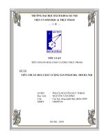
3.2.2 Density Evaluation A wide variety of materials
and processes have been used to create substrates for electronics over the last half century, from traditional printed
circuits made from resins (i.e., epoxy), reinforcements (i.e.,
glass cloth or paper), and metal foil (i.e., copper), to ceramics metallized by various thin and thick film techniques.
However, they all share a common attribute; they must
route signals through conductors.
There are also limits to how much routing each can accommodate. The factors that define the limits of their wire
routing ability as a substrate are:
• Pitch/distance between vias or holes in the substrate.
• Number of wires that can be routed between those vias.
• Number of signal layers required.
In addition, the methods of producing blind and buried vias
can facilitate routing by selectively occupying routing
channels. Vias that are routed completely through the
printed board preclude any use of that space for routing on
all conductor layers.
These factors can be combined to create an equation that
defines the wire routing ability of a technology. In the past,
most components had terminations along the periphery on
two or more sides. However area array components are
more space conservative and allow coarser I/O pitches to
be used (see Figure 3-1).
3.3 Schematic/ Logic Diagram The initial schematic/
logic diagram designates the electrical functions and interconnectivity to be provided to the designer for the printed
board and its assembly. This schematic should define, when
applicable, critical circuit layout areas, shielding requirements, grounding and power distribution requirements, the
allocation of test points, and any preassigned input/output
connector locations. Schematic information may be generated as hard copy or computer data (manually or automated).
3.4 Parts List A parts list is a tabulation of parts and
materials used in the construction of a printed board assembly. All end item identifiable parts and materials shall be
identified in the parts list or on the field of the drawing.
Excluded are those materials used in the manufacturing
process, but may include reference information; i.e., specifications pertinent to the manufacture of the assembly and
reference to the schematic/logic diagram.
May 2003
IPC-2221A
1600
1400
I/O Count
1200
Array Package
0.5 mm [ 0.020 in] pitch
1000
800
Array Package
0.7 mm [0.028 in] pitch
600
400
Array Package
1.0 mm [0.0394 in] pitch
200
0
1 mm
[0.039 in]
Peripheral Lead
0.5 mm [0.020 in] pitch
5 mm
[0.20 in]
10 mm
[0.394 in]
15 mm
[0.591 in]
Package or Die Edge
20 mm
[0.787 in]
IPC-2221a-3-02
Figure 3-1 Package Size and I/O Count
All mechanical parts appearing on the assembly pictorial
shall be assigned an item number which shall match the
item number assigned on the parts list.
Electrical components, such as capacitors, resistors, fuses,
ICs, transistors, etc., shall be assigned reference designators, (Ex. C5, CR2, F1, R15, U2, etc.). Assignment of electrical reference designators shall be the same as (match)
those assignments given to the same components on the
Logic/schematic diagram.
It is advisable to group like items; e.g., resistors, capacitors, ICs, etc., in some sort of ascending or numerical
order.
The parts list may be handwritten, manually typed on to a
standard format, or computer generated.
3.5 Test Requirement Considerations Normally, prior
to starting a design, a testability review meeting should be
held with fabrication, assembly, and testing. Testability
concerns, such as circuit visibility, density, operation, circuit controllability, partitioning, and special test requirements and specifications are discussed as a part of the test
strategy. See Appendix A for a checklist of design for testability criteria.
During the design testability review meeting, tooling concepts are established, and determinations are made as to the
most effective tool-cost versus board layout concept conditions.
During the layout process, any circuit board changes that
impact the test program, or the test tooling, should immediately be reported to the proper individuals for determination as to the best compromise. The testing concept should
develop approaches that can check the board for problems,
and also detect fault locations wherever possible. The test
concept and requirements should economically facilitate
the detection, isolation, and correction of faults of the
design verification, manufacturing, and field support of the
printed board assembly life cycle.
3.5.1 Printed Board Assembly Testability Design of a
printed board assembly for testability normally involves
systems level testability issues. In most applications, there
are system level fault isolation and recovery requirements
such as mean time to repair, percent up time, operate
through single faults, and maximum time to repair. To meet
the contractual requirements, the system design may
include testability features, and many times these same features can be used to increase testability at the printed board
assembly level. The printed board assembly testability philosophy also needs to be compatible with the overall integrations, testing and maintenance plans for the contract.
The factory testers to be used, how integration and test is
planned, when printed board assemblies are conformal
coated, the depot and field test equipment capabilities and
personnel skill level are all factors that must be considered
when developing the printed board assembly test strategy.
The test philosophy may be different for different phases of
the program. For example, the first unit debug philosophy
may be much different than the test philosophy for spares
when all the systems have already been shipped.
Before the PCB design starts, requirements for the system
testability functions should be presented at the conceptual
design review. These requirements and any derived requirements should be partitioned down to the various printed
board assemblies and documented. The system and program level test criteria and how they are partitioned down
to the printed board assembly requirements are beyond the
scope of this document. Appendix A provides an example
of a checklist to be used in evaluating the testability of the
design.
7
IPC-2221A
The two basic types of printed board assembly test are
functional test and in-circuit test. Functional testing is used
to test the electrical design functionality. Functional testers
access the board under test through the connector, test
points, or bed-of-nails. The board is functionally tested by
applying pre-determined stimuli (vectors) at the printed
board assembly’s inputs while monitoring the printed board
assembly outputs to ensure that the design responds properly.
In-circuit testing is used to find manufacturing defects in
printed board assemblies. In-circuit testers access the board
under test through the use of a bed-of-nails fixture which
makes contact with each node on the printed board assembly. The printed board assembly is tested by exercising all
the parts on the board individually. In-circuit testing places
less restrictions on the design. Conformal coated printed
board assemblies and many Surface Mount Technology
(SMT) and mixed technology printed board assemblies
present bed-of-nails physical access problems which may
prohibit the use of in-circuit testing. Primary concerns for
in-circuit test are that the lands or pins (1) must be on grid
(for compatibility with the use of bed-of-nails fixture) and
(2) should be accessible from the bottom side (a.k.a. noncomponent or solder side of through-hole technology
boards) of the printed board assembly.
Manufacturing Defects Analyzer (MDA) provide a low
cost alternative to the traditional in-circuit tester. Like the
in-circuit tester, the MDA examines the construction of the
printed board assembly for defects. It performs a subset of
the types of tests, mainly only tests for shorts and opens
faults without power applied to the printed board assembly.
For high volume production with highly controlled manufacturing processes (i.e., Statistical Process Control techniques), the MDA may have application as a viable part of
a printed board assembly test strategy.
Vectorless Test is another low cost alternative to in-circuit
testing. Vectorless Test performs testing for finding manufacturing process-related pin faults for SMT boards and
does not require programming of test vectors. It is a
powered-off measurement technique consisting of three
basic types of tests:
1. Analog Junction Test – DC current measurement test on
unique pin pairs of the printed board assembly using the
ESD protection diodes present on most digital and
mixed signal device pins.
2. RF Induction Test – Magnetic induction is used to test
for device faults utilizing the printed board assemblies
devices protection diodes. This technique uses chips
power and ground pins to make measurements for finding solder opens on device signal paths, broken bond
wires, and devices damaged by ESD. Parts incorrectly
oriented can also be detected. Fixturing containing magnetic inducers are required for this type of test.
8
May 2003
3. Capacitive Coupling Test – This technique uses capacitive coupling to test for pin opens and does not rely on
internal device circuitry but instead relies on the presence of the metallic lead frame of the device to test the
pins. Connectors and sockets, lead frames and correct
polarity of capacitors can be tested using the technique.
3.5.2 Boundary Scan Testing As printed board assemblies become more dense with fine pitch devices, physical
access to printed board assembly nodes for in-circuit testing may not be possible. The boundary scan standard for
integrated circuits (IEEE 1149.1) provides the means to
perform virtual in-circuit testing to alleviate this problem.
Boundary scan architecture is a scan register approach
where, at the cost of a few I/O pins and the use of special
scan registers in strategic locations throughout the design,
the test problem can be simplified to testing of simpler,
mostly combinational circuits.
In many applications, the inclusion of scan registers on the
inputs and outputs of the printed board assembly allows the
board to be tested while installed. If the circuit is more
complex, additional sets of scan registers can be included
in the design to capture intermediate results and apply test
vectors to exercise portions of the design.
A full description of the standard access port and boundary
scan architecture can be found in IEEE 1149.1. The full
test access port capabilities are not needed to gain significant testability via the scan registers.
The decision to use boundary scan test as part of a test
strategy should consider the availability of boundary scan
parts and the return on investment for capital equipment
and software tools required for implementing this test technique. Boundary scan testing can be conducted using a low
cost PC-based tester which requires access to the printed
board assembly under test through the edge connector or an
existing functional, in-circuit, or hybrid tester that may be
adapted to perform boundary scan testing.
3 .5 .3 Funct ional Te st Conce rn for Print e d Board
Assemblies There are several concerns for designing the
printed board assembly for functional testability. The use of
test connectors, problems with initialization and synchronization, long counter chains, self diagnostics, and physical
testing are topics which are discussed in detail in the following subsections and are not meant to be tutorials on
testability but rather ideas of how to overcome typical
functional testing problems.
3.5.3.1 Test Connectors Fault isolation on conformal
coated boards or most SMT and mixed technology designs
can be very difficult because of the lack of access to the
circuitry on the board.
If strategic signals are brought out to a test connector or an
area on the printed board where the signals can be probed
May 2003
(test points), fault isolation may be much improved. This
lowers the cost of detection, isolation and correction.
It is also possible to design the circuit so that a test connector can be used to stimulate the circuit (such as taking
over a data bus via the test connector) or disable functions
on the printed board assembly (such as disabling a free
running oscillator and adding single step capability via the
test connector).
3.5.3.2 Initialization and Synchronization Some designs
or portions of a design do not need any initialization circuitry because the circuit will quickly cycle into its
intended function. Unfortunately, it is sometimes very difficult to synchronize the tester with this type of circuit
because the tester would need to be programmed to stimulate the circuit until a predetermined signature is found on
the outputs of the circuit. This can be difficult to achieve.
With relatively little difference in the design, initialization
capability can usually be designed into the circuitry allowing the printed board assembly to be quickly initialized and
the circuit and the tester can follow the expected outputs of
the printed board assembly.
Free running oscillators also present a problem in testing
because of the synchronization problem with the test equipment. These problems can be overcome by (1) adding test
circuitry to select a test clock instead of the oscillator; (2)
removing the oscillator for test and injecting a test clock;
(3) overriding the signal; or (4) designing the clock system
so that the clocking can be controlled via a test connector
or test points.
Long counter chains in the
design with signals used from many stages of the counter
chain present another testability problem. Testability can be
very bad if there is no means to preset the counter chain to
different values to facilitate testing of the logic that is
driven from the high order stages of the counter chain.
3.5.3.3 Long Counter Chains
Testability is much improved if the counter chain is either
broken into smaller counter chains (perhaps no more than
10 stages) which can be individually controlled or if the
counter chain can be loaded via the test software. The test
software can then verify the operation of the logic that is
driven from the counter stages without wasting the simulation and test time that would be required to clock through
the complete counter chain.
Self diagnostics are sometimes
imposed either contractually or via derived requirements.
Careful consideration should be given to determine how to
implement these requirements.
3.5.3.4 Self Diagnostics
Many times a printed board assembly does not contain
functions that lend themselves to self diagnostics at the
printed board assembly level but a small group of printed
board assemblies, when taken as a unit, do lend themselves
IPC-2221A
to good diagnostics. For example, a complex Fast Fourier
Transform (FFT) function may be spread across multiple
printed board assemblies. It may be very difficult for any
one printed board assembly to self diagnose a problem but
it may be very easy to design-in circuitry that self diagnoses the whole FFT function.
The depth of self diagnostics that are needed is usually
driven by the line replaceable unit (LRU) which varies
with requirements. It may be an integrated circuit or it may
be a drawer of electronics depending on the contract, the
function of the design, or the system level maintenance
philosophy.
For self diagnostics at a printed board assembly level, the
printed board assembly is usually put into a test mode and
then the printed board assembly applies a known set of test
inputs and compares the results with a stored set of
expected responses. If the results do not match the
expected responses, the printed board assembly signals the
test equipment indicating the printed board assembly failed
the self-test. There are many variations on this scheme.
Some examples are:
1. The printed board assembly is placed in a feedback loop
with the results checked after a predetermined number
of cycles.
2. A special test circuit or the Central Processor Unit
(CPU) applying the stimuli and comparing the signature
of the responses against a known pattern.
3. The printed board assembly performing self-checks
when idling and then supplying the results to another (or
diagnostic) printed board assembly for verification of
the responses, etc.
Printed board assembly
functional test equipment is usually very expensive and
requires highly skilled personnel to operate. If printed
board assembly testability is poor, the printed board assembly test operation can be very expensive. There are some
simple physical considerations that can decrease the debug
time and therefore the overall test costs.
3.5.3.5 Physical Test Concerns
The orientation of polarized parts should be consistent so
that the operator does not get confused with parts being
oriented 180° out of phase with other parts on the printed
board assembly. Nonpolarized parts still need to have the
pin #1 identified so that the test operator knows which end
to probe when guided probe software says to probe a specific pin.
Test connectors are much preferred over test points which
require the use of test clips or test hook-up wires. However,
test points such as riser leads are preferred over clipping on
to the lead of a part. If riser leads are used for temporary
testing, such as determining a select-by-test resistor, it is
suggested that the risers remain after the installation of the
selected component. This allows verification of the selected
item without re-fixturing the assembly.
9
IPC-2221A
Signals that are not accessible for probing (such as can
happen with leadless parts) can greatly increase fault isolation problems. If scan registers are not used, it is recommended that every signal have a land or other test point
somewhere on the printed board assembly where the signal
can be probed. It is also recommended that lands used for
test points be located on grid and placed so that all the
probing can be done from the secondary side of the printed
board assembly. If it is not feasible to provide capability
for probing every signal, then (1) only the strategic signals
should have special probing locations and (2) the test vectors need to be increased or other test techniques need to be
utilized to assign fault isolation to one component or a
small set of components.
Many faults are often due to shorts between the leads of
adjacent parts, shorts between a part lead and an external
layer conductor on the printed board or shorts between two
printed board conductors on the external layers of the
printed board. The physical design must consider these normal manufacturing defects and not impair the isolation of
the faults due to lack of access or inconvenient access to
signals. As with design for in-circuit testability, probe pad
test points should be on grid to allow automated probing to
be used in the future.
Partitioning of the design into functions, perhaps digital
separated from analog, is sometimes required for electrical
performance. Testing concerns also are helped with physical separation of dissimilar functions. Separation of not just
the circuitry but also the test connectors or at least grouping the pins on the connectors can help improve testability.
Designs that mix digital design with high performance analog design may require testing on two or more sets of test
equipment. Separating the signals will not only help the
test fixturing but will help the operator in debugging the
printed board assembly.
As with in-circuit test fixturing, functional test fixturing
can have a significant cost impact. Normally a standard
board size or only a few board sizes are used for all designs
on a program. Similarly one, or at most a few, test fixtures
are typically used for a program. Generating test fixtures
can be costly and debugging noise problems in the fixtures
or tuning the fixtures to the tester can be expensive. If the
test fixturing is not adequately engineered, it may not be
possible to accurately measure the board under test. Typically much effort is expended in generating a few test fixtures and it is expected that the fixtures will be used for all
the printed board assembly designs. Therefore the test fixturing restrictions must be considered in the printed board
assembly design. The fixturing restraints can be significant.
Such as (1) requiring ground and voltage supplies on specific connector pins, (2) limiting which pins can be used for
high speed signals, (3) limiting which pins can be used for
10
May 2003
low noise applications, (4) defining power switching limitations, (5) defining voltage and current limitations on each
pin, etc.
3 .5 .4 In- Circuit Te st Conce rns for Print e d Board
Assemblies In-circuit testing is used to find shorts,
opens, wrong parts, reversed parts, bad devices, incorrect
assembly of printed board assemblies and other manufacturing defects. In-circuit testing is neither meant to find
marginal parts nor to verify critical timing parameters or
other electrical design functions.
In-circuit testing of digital printed board assemblies can
involve a process that is known as backdriving (see IPC-T50). Backdriving can also cause devices to oscillate and the
tester can have insufficient drive to bring a device out of
saturation. Backdriving can be performed only for controlled periods of time, or the junction of the device (with
the overdriven output) will overheat.
The two main concerns for designing the printed board and
printed board assembly for in-circuit testability are design
for compatibility with in-circuit test fixturing and electrical
design considerations. These topics are discussed in detail
in the following subsections.
In-circuit test fixtures
are commonly called bed-of-nails fixtures. A bed-of-nails
fixture is a device with spring contact probes which contact
each node on the board under test. The following guidelines should be followed during printed board assembly
layout to promote in-circuit testability in bed-of-nails fixtures:
3.5.4.1 In-Circuit Test Fixtures
1. The diameter of lands of plated-through holes and vias
used as test lands are a function of the hole size (see
9.1.1). The diameter of test lands used specifically for
probing should be no smaller than 0.9 mm [0.0354 in].
It is feasible to use 0.6 mm [0.0236 in] diameter test
lands on boards under 7700 mm2 [11.935 in2].
2. Clearances around test probe sites are dependent on
assembly processes. Probe sites should maintain a
clearance equal to 80% of an adjacent component
height with a minimum of 0.6 mm [0.0236 in] and a
maximum of 5 mm [0.20 in] (see Figure 3-2).
3. Part height on the probe side of the board must not
exceed 5.7 mm [0.224 in]. Taller parts on this side of
the board will require cutouts in the test fixture. Test
lands should be located 5 mm [0.20 in] away from tall
components. This allows for test fixture profiling tolerances during test fixture fabrication (see Figure 3-3).
4. No parts or test lands are to be located within 3 mm of
the board edges.
5. All probe areas must be solder coated or covered with
a conductive nonoxidizing coating. The test lands must
be free of solder resist and markings.
May 2003
IPC-2221A
0.6 mm [0.0236 in]
FREE AREA
SIDE
VIEW
TOP
VIEW
TEST
•
PPD
TEST
LAND
0.6 mm
[0.0236 in]
0.6 mm
[0.0236 in]
COMPONENT FREE AREA
IPC-2221a-3-02
Figure 3-2 Test Land Free Area for Parts and Other Intrusions
COMPONENT
HEIGHT
>5.7 mm
[>0.224 in]
FREE
AREA
TEST
•
PPD
5 mm [0.20 in]
TALL COMPONENT
FREE AREA
5 mm
[0.20 in]
IPC-2221a-3-03
Figure 3-3 Test Land Free Area for Tall Parts
6. Probe the test lands or vias, not the termination/
castellations of leadless surface mount parts or the
leads of leaded parts (see Figure 3-4). Contact pressure
can cause an open circuit or make a cold solder joint
appear good.
7. Avoid requiring probing of both sides of the printed
board. Use vias, to bring test points to one side, the
bottom side (noncomponent or solder side of throughhole technology printed board assemblies) of the
board. This allows for a reliable and less expensive
fixture.
APPLICATIONS
INCORRECT
INCORRECT
CORRECT
CORRECT
8. Test lands should be on 2.5 mm [0.0984 in] hole centers, if possible, to allow the use of standard probes
and a more reliable fixture.
9. Do not rely on edge connector fingers for test lands.
Gold plated fingers are easily damaged by test probes.
10. Distribute the test lands evenly over the board area.
When the test lands are not evenly distributed or when
they are concentrated in one area, the results are board
flexing, probing faults, and vacuum sealing problems.
IPC-2221a-3-04
Figure 3-4 Probing Test Lands
11
IPC-2221A
11. A test land must be provided for all nodes. A node is
defined as an electrical connection between two or
more components. A test land requires a signal name
(node signal name), the x-y position axis in respect to
the printed board datum point, and a location (describing which side of the board the test land is located).
This data is required to build a fixture for SMT and
mixed technology printed board assemblies.
12. Mixed technology printed board assemblies and pin
grid component boards provide test access for some
nodes at the solder side pins. Pins and vias used at test
lands must be identified with node signal name and x-y
position in reference to the printed board datum point.
Use solder mount lands of parts and connectors as test
points to reduce the number of generated test lands.
The following electrical considerations should be followed during
printed board assembly layout to promote in-circuit testability:
3.5.4.2 In-Circuit Electrical Considerations
1. Do not wire control line pins directly to ground, Vcc, or
a common resistor. Disabled control lines on a device
can make it impossible to use the standard in-circuit
library tests. A specialized test with reduced fault coverage and higher program cost is the normal result.
2. A single input vector for tri-stating a device’s outputs is
preferable for in-circuit testing. Reasons for tri-statable
outputs are (1) testers have a limited amount of vectors,
(2) the backdrive problems will disappear, and (3) it
simplifies the generation of test programs. An example
of this which would reduce program cost is tri-statable
Programmable Array Logic (PAL) outputs. Use a spare
input to a pull-up resistor plus an equation that would
enable a normal function in a high state and the device
outputs to be tri-stated in a low state.
3. Gate arrays and devices with high pin counts are not
testable using an in-circuit tester. Backdrive may not be
a problem per pin but the large numbers of pins limit
backdrive restrictions. A control line or a single vector
to tri-state all device outputs is recommended.
4. Node access and the inability to cover all nodes using
standard in-circuit testers is a growing problem. If standard test techniques cannot be applied to detect surface
mounted part faults, an alternative method must be
developed.
May 2003
face mount printed board assembly area. IEEE Standard
1149.1 is the specification for boundary scan.
3.5.5 Mechanical
Test fixtures are most
often designed for automatic or semiautomatic engagement
of edge type or on-board connectors. Connectors should be
positioned to facilitate quick engagement and should be
uniform and consistent (standardized) in their relationships
to the board from one design to another. Similar types of
connectors should be keyed, or board geometry used, to
ensure proper mating, and prevent electrical damage to the
circuitry.
3.5.5.1 Uniformity of Connectors
3.5.5.2 Uniformity of Power Distribution Arrangement
and Signal Levels on Connectors The connector contact
position should be uniform for AC and DC power levels,
DC common and chassis ground, e.g., contact number 1 is
always connected to the same relative circuit power point
in each board design. Standardizing contact positions will
minimize test fixture cost and facilitate diagnostics.
Signals of widely different magnitude should be isolated to
minimize crosstalk.
Logic levels should be located in pre-designated connector
contacts.
3.5.6 Electrical
3.5.6.1 Bare Board Testing Bare board testing shall be
performed in accordance with IPC-9252. If testing will use
data from the design area, the configuration and type of
data provided will be determined by the method of test
selected.
Bare board testing is performed by the printed board supplier and includes continuity, insulation resistance and
dielectric withstanding voltage. Suppliers can also perform
testing of controlled impedance circuitry. Continuity tests
are performed to assure conductors are not broken (opens)
or inadvertently connected together (shorts). Insulation
resistance and dielectric withstanding voltage testing is performed to assure sufficient conductor spacing and dielectric
thickness.
Alternative test strategies must be developed for SMT
printed board assemblies with limited nodes. An example
of this is a test that will partition the board into groups of
clustering components. Each group must have control lines
(for testability) and test lands to electrically isolate the
cluster from the other devices or groups during test.
There are two basic types of continuity testing; Golden
Board and Intelligent. In Golden Board test, a known good
board is tested and its results are used to test all the remaining boards in the lot. If there were an error in the Golden
Board, an error in all boards could go undetected. The
Intelligent test verifies each board against the design’s electrical net list. It will not miss the defects which could be
undetected in a Golden Board test.
Another alternative test method for opens, shorts, and correct devices is boundary scan. This built-in-test-circuitry
(electronic bed-of-nails) is gaining momentum in the sur-
Designs which do not have all electrical connections available from one side of the board (such as boards with blind
or buried vias, components on both sides with via holes
12
May 2003
solder resist tented or boards bonded to both sides of heatsinks) will require Flip or Clamshell testing. Flip testing
tests one side of the board and then the other on two separate fixtures. Connections which require contacting both
sides of the board are not evaluated. Clamshell testing uses
two fixtures which come in contact with both sides of the
board at the same time and is capable of testing all connections. Flip and Clamshell testing costs more than testing
performed from one side of the board only.
The following areas shall be considered before starting a
design.
3.5.6.2 Testing Surface Mount Patterns Normally, testing of a bare board involves fixturing where spring loaded
pins contact plated holes. On a surface mount pattern, the
ends of the nets are typically not at holes but rather on surface mount lands. There are at least two different strategies
for performing testing:
A. Contact the via which is connected to the land and
visually inspect to ensure continuity from the via to the
land. Vias can be designed such that they are on a common grid which will reduce the need for special fixturing for each part number. The barrels of the platedthrough holes that are used for internal electrical
connectivity should not be subject to probing unless the
force is very low and the point of the probe will not
damage the barrel. These barrels can crack or break
free from the land on the internal layer if subjected to
mechanical stresses.
B. Test to the land itself. This approach will probably
require special fixturing since surface mount lands may
not all be on a grid. Additionally, computer design systems may place the end-of-net point at a via rather than
the land which may require adjustment of test point
locations.
3.5.6.3 Testing of Paired Printed Boards Laminated to a
Core At least two approaches are available for electrical
test:
A. Test the top and bottom of the laminated composite
printed board separately. If there are plated holes which
provide a side-to-side interconnection, they will require
a manual electrical test or visual inspection to ensure
hole continuity.
B. Use a clam shell type fixture where both the top and
bottom of the composite printed board can be tested
together. The use of the first approach will require that
the electrical test data be provided in two parts. When
networks have terminations on both sides of the printed
board, the electrical test data should be split into at
least two parts with the end of net occurring at the
side-to-side interconnect. ‘‘Self learn’’ testing from a
known good board will provide the data automatically
in the above format.
IPC-2221A
3.5.6.4 Point of Origin Electrical test and numerical control data should have a common origin point for ease of
constructing electrical test fixtures.
3.5.6.5 Test Points When required by the design, test
points for probing shall be provided as part of the conductor pattern and shall be identified on the drawing set. Vias,
wide conductors, or component lead mounting lands may
be considered as probe points provided that sufficient area
is available for probing and maintaining the integrity of the
via, conductor, or component lead mounting joint. Probe
points must be free of nonconductive coating materials
such as solder resist or conformal coating.
3.6 Layout Evaluation
The design layout from one
board design to another should be such that designatedareas are identified by function, e.g., power supply section
confined to one area, analog circuits to another section, and
logic circuits to another, etc. This will help to minimize
crosstalk, simplify bare board and assembly test fixture
design, and facilitate troubleshooting diagnostics. In addition, the design should:
3.6.1 Board Layout Design
• Ensure that components have all testable points accessible
from the secondary side of the board to facilitate probing
with single-sided test fixtures.
• Have feed-throughs and component holes placed away
from board edges to allow adequate test fixture clearance.
• Require the board be laid out on a grid which matches the
design team testing concept.
• Allow provision for isolating parts of the circuit to facilitate testing and diagnostics.
• Where practical, group test points and jumper points in
the same physical location on the board.
• Consider high-cost components for socketing so that parts
can be easily replaced.
• Provide optic targets (fiducials) for surface mount designs
to allow the use of optic positioning and visual inspection
equipment and methods (see 5.4.3).
Surface mounted components and their patterns require
special consideration for test probe access, especially if
components are mounted on both sides of the board and
have very high lead counts.
3 .6 .1 .1 Layout Concepts The printed board layout
depicts the physical size and location of all electronic and
mechanical components, and the routing of conductors that
electrically interconnect the components in sufficient detail
to allow the preparation of documentation and artwork.
3 .6 .2 Feasibility Density Evaluation After approved
documents for schematic/logic diagrams, parts lists, and
end-product and testing requirements are provided, and
13
IPC-2221A
May 2003
before the actual drawing of the layout is begun, a feasibility density evaluation should be made. This should be
based on the maximum size of all parts required by the
parts list and the total space they and their lands will
require on the board, exclusive of interconnection conductor routing.
The total board geometry required for this mounting and
termination of the components should then be compared to
the total usable board area for this purpose. Reasonable
maximum values for this ratio are 70% for Level A, 80%
for Level B, and 90% for Level C. Component density values higher than these will be a cause for concern. The
lower these values are, the easier it will be to design a
cost-effective functional board.
Table 3-2 gives the area (in 0.5 mm [0.020 in] grid elements) a component will occupy on the board for a variety
of components. As an example, the 14 lead dual in-line
package for through-hole technology occupies a total of
84.0 grid elements. The package outline that encloses the
component and land pattern has a grid matrix of 20 x 42
grid elements on 0.5 mm [0.020] centers. The 20 grid elements establish an outline dimension of 10 mm [0.394 in]
while the 42 grid elements account for 21 mm [0.827 in].
This component area would use up a portion of the board
usable area. The component outline does not include grid
elements for conductor routing outside the land area. Total
component area compared to total usable area provides the
conductor routing availability and thus the density percentage.
Figure 3-5 provides the usable board area for the standardized board sizes recommended in Figure 5-1.
An alternative method of feasibility density evaluation
expresses board density in units of square centimeters per
Overall Dimensions
Board Size
(Fig. 5-1)
Height
mm [in]
Width
mm [in]
Usable Dimensions
Height
mm [in]
Width
mm [in]
Usable Area
mm2
Grid Elements
0.5 mm Grid
cm2
A1
80 [3.15]
65 [2.56]
3200
12800
32
B1
170 [6.692]
155 [6.102]
7700
30800
77
C1
260 [10.25]
12200
48800
122
D1
350 [13.78]
335 [13.19]
16700
66800
167
A2
80 [3.15]
65 [2.56]
7100
28400
71
17000
68000
170
26900
107600
269
60 [2.36]
245 [9.646]
B2
170 [6.692]
C2
260 [10.25]
D2
350 [13.78]
335 [13.19]
36800
147200
368
A3
80 [3.15]
65 [2.56]
11000
44000
110
26300
105200
263
41600
166400
416
120 [4.724]
155 [6.102]
50 [1.97]
245 [9.646]
B3
170 [6.692]
C3
260 [10.25]
D3
350 [13.78]
335 [13.19]
56900
227600
569
A4
80 [3.15]
65 [2.56]
14900
59600
149
B4
170 [6.692]
35600
142400
356
C4
260 [10.25]
56300
225200
563
D4
350 [13.78]
77000
308000
770
180 [7.087]
240 [9.449]
155 [6.102]
110 [4.331]
245 [9.646]
155 [6.102]
245 [9.646]
170 [6.693]
230 [9.055]
335 [13.19]
5.0
[0.197]
TYP
Tooling Holes
0/0 Fiducial
5.0 [0.197] TYP
Usable Area
Connector
5.0
[0.197]
TYP
10.0
[0.394]
TYP
Area
IPC-2221a-3-05
Figure 3-5 Example of Usable Area Calculation, mm [in] (Usable area determination includes clearance allowance for
edge-board connector area, board guides, and board extractor.)
14
May 2003
IPC-2221A
Table 3-2 Component Grid Areas
Number of Grid Elements2
0.5 mm [0.20 in] Grid
Component Description
Type1
D07 (without stress relief loop)
THT
6 x 24
144
D07 (with stress relief loop)
THT
6 x 28
168
T05
THT
20 x 20
400
T024
THT
10 x 10
100
CK05
THT
6 x 12
72
CM05, 13000pF
THT
20 x 44
880
CM06, 400pF
THT
12 x 26
312
RC07
THT
6 x 20
120
RC20
THT
10 x 26
260
RN60
THT
10 x 30
300
CQFP-10 T090
SMT
16 x 12
192
CQFP-28
SMT
34 x 34
1156
CQFP-144
SMT
68 x 68
4624
3216 (1206)
SMT
4 x 10
40
4564 (1825)
SMT
14 x 12
168
6032
SMT
8 x 18
144
DIP-14
THT
20 x 42
840
DIP-14
SMT
22 x 42
924
DIP-24
SMT
22 x 60
1320
DIP-24L
SMT
26 x 64
1664
SOD87/MLL-41
SMT
6 x 14
84
SOT23
SMT
8x8
64
SOT89
SMT
12 x 10
120
SOT143
SMT
8x8
64
SQFP 7x7-40
SMT
22 x 22
484
SOIC-20W
SMT
28 x 24
672
SOIC-36X
SMT
48 x 24
1152
TSOP 10x20
SMT
22 x 44
968
SOJ 26/350
SMT
24 x 34
816
1
THT = Through-Hole Technology, SMT = Surface Mount Technology
Grid area includes physical component outlines and land areas. It does not include space for conductor routing.
2
equivalent SOIC. A 16-pin SOIC occupies approximately
one cm2 of board area. Figure 3-6 shows a table for determining the SOIC equivalent for a variety of components
and the total SOIC equivalents used on the board. This
number is then divided into the total square centimeters of
usable board area. Reasonable maximum density values are
0.55 cm2 per SOIC for Level A, 0.50 for Level B, and 0.45
for Level C. Density values can increase with additional
circuit layers. Also, when using surface mount technology,
the potential usable board area is theoretically doubled.
Finished printed boards
shall meet the performance requirements of IPC-6011 and
its applicable sectional specification.
3.7 Performance Requirements
15