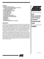
ĐIỆN tử VIỄN THÔNG AT89S51 en khotailieu
Bạn đang xem bản rút gọn của tài liệu. Xem và tải ngay bản đầy đủ của tài liệu tại đây (202 KB, 27 trang )
Features
• Compatible with MCS-51® Products
• 4K Bytes of In-System Programmable (ISP) Flash Memory
•
•
•
•
•
•
•
•
•
•
•
•
•
•
•
– Endurance: 1000 Write/Erase Cycles
4.0V to 5.5V Operating Range
Fully Static Operation: 0 Hz to 33 MHz
Three-level Program Memory Lock
128 x 8-bit Internal RAM
32 Programmable I/O Lines
Two 16-bit Timer/Counters
Six Interrupt Sources
Full Duplex UART Serial Channel
Low-power Idle and Power-down Modes
Interrupt Recovery from Power-down Mode
Watchdog Timer
Dual Data Pointer
Power-off Flag
Fast Programming Time
Flexible ISP Programming (Byte and Page Mode)
Description
The AT89S51 is a low-power, high-performance CMOS 8-bit microcontroller with 4K
bytes of in-system programmable Flash memory. The device is manufactured using
Atmel’s high-density nonvolatile memory technology and is compatible with the industry-standard 80C51 instruction set and pinout. The on-chip Flash allows the program
memory to be reprogrammed in-system or by a conventional nonvolatile memory programmer. By combining a versatile 8-bit CPU with in-system programmable Flash on a
monolithic chip, the Atmel AT89S51 is a powerful microcontroller which provides a
highly-flexible and cost-effective solution to many embedded control applications.
8-bit
Microcontroller
with 4K Bytes
In-System
Programmable
Flash
AT89S51
The AT89S51 provides the following standard features: 4K bytes of Flash, 128 bytes of
RAM, 32 I/O lines, Watchdog timer, two data pointers, two 16-bit timer/counters, a fivevector two-level interrupt architecture, a full duplex serial port, on-chip oscillator, and
clock circuitry. In addition, the AT89S51 is designed with static logic for operation
down to zero frequency and supports two software selectable power saving modes.
The Idle Mode stops the CPU while allowing the RAM, timer/counters, serial port, and
interrupt system to continue functioning. The Power-down mode saves the RAM contents but freezes the oscillator, disabling all other chip functions until the next external
interrupt or hardware reset.
Rev. 2487A–10/01
1
Pin Configurations
PLCC
VCC
P0.0 (AD0)
P0.1 (AD1)
P0.2 (AD2)
P0.3 (AD3)
P0.4 (AD4)
P0.5 (AD5)
P0.6 (AD6)
P0.7 (AD7)
EA/VPP
ALE/PROG
PSEN
P2.7 (A15)
P2.6 (A14)
P2.5 (A13)
P2.4 (A12)
P2.3 (A11)
P2.2 (A10)
P2.1 (A9)
P2.0 (A8)
(MOSI) P1.5
(MISO) P1.6
(SCK) P1.7
RST
(RXD) P3.0
NC
(TXD) P3.1
(INT0) P3.2
(INT1) P3.3
(T0) P3.4
(T1) P3.5
6
5
4
3
2
1
44
43
42
41
40
40
39
38
37
36
35
34
33
32
31
30
29
28
27
26
25
24
23
22
21
7
8
9
10
11
12
13
14
15
16
17
39
38
37
36
35
34
33
32
31
30
29
18
19
20
21
22
23
24
25
26
27
28
1
2
3
4
5
6
7
8
9
10
11
12
13
14
15
16
17
18
19
20
P0.4 (AD4)
P0.5 (AD5)
P0.6 (AD6)
P0.7 (AD7)
EA/VPP
NC
ALE/PROG
PSEN
P2.7 (A15)
P2.6 (A14)
P2.5 (A13)
(WR) P3.6
(RD) P3.7
XTAL2
XTAL1
GND
NC
(A8) P2.0
(A9) P2.1
(A10) P2.2
(A11) P2.3
(A12) P2.4
P1.0
P1.1
P1.2
P1.3
P1.4
(MOSI) P1.5
(MISO) P1.6
(SCK) P1.7
RST
(RXD) P3.0
(TXD) P3.1
(INT0) P3.2
(INT1) P3.3
(T0) P3.4
(T1) P3.5
(WR) P3.6
(RD) P3.7
XTAL2
XTAL1
GND
P1.4
P1.3
P1.2
P1.1
P1.0
NC
VCC
P0.0 (AD0)
P0.1 (AD1)
P0.2 (AD2)
P0.3 (AD3)
PDIP
44
43
42
41
40
39
38
37
36
35
34
P1.4
P1.3
P1.2
P1.1
P1.0
NC
VCC
P0.0 (AD0)
P0.1 (AD1)
P0.2 (AD2)
P0.3 (AD3)
TQFP
33
32
31
30
29
28
27
26
25
24
23
1
2
3
4
5
6
7
8
9
10
11
P0.4 (AD4)
P0.5 (AD5)
P0.6 (AD6)
P0.7 (AD7)
EA/VPP
NC
ALE/PROG
PSEN
P2.7 (A15)
P2.6 (A14)
P2.5 (A13)
(WR) P3.6
(RD) P3.7
XTAL2
XTAL1
GND
GND
(A8) P2.0
(A9) P2.1
(A10) P2.2
(A11) P2.3
(A12) P2.4
12
13
14
15
16
17
18
19
20
21
22
(MOSI) P1.5
(MISO) P1.6
(SCK) P1.7
RST
(RXD) P3.0
NC
(TXD) P3.1
(INT0) P3.2
(INT1) P3.3
(T0) P3.4
(T1) P3.5
2
AT89S51
2487A–10/01
AT89S51
Block Diagram
P0.0 - P0.7
P2.0 - P2.7
PORT 0 DRIVERS
PORT 2 DRIVERS
VCC
GND
RAM ADDR.
REGISTER
B
REGISTER
PORT 0
LATCH
RAM
PORT 2
LATCH
FLASH
PROGRAM
ADDRESS
REGISTER
STACK
POINTER
ACC
BUFFER
TMP2
TMP1
PC
INCREMENTER
ALU
INTERRUPT, SERIAL PORT,
AND TIMER BLOCKS
PROGRAM
COUNTER
PSW
PSEN
ALE/PROG
EA / VPP
TIMING
AND
CONTROL
INSTRUCTION
REGISTER
DUAL DPTR
RST
WATCH
DOG
PORT 3
LATCH
PORT 1
LATCH
ISP
PORT
PROGRAM
LOGIC
OSC
PORT 3 DRIVERS
P3.0 - P3.7
PORT 1 DRIVERS
P1.0 - P1.7
3
2487A–10/01
Pin Description
VCC
Supply voltage.
GND
Ground.
Port 0
Port 0 is an 8-bit open drain bidirectional I/O port. As an output port, each pin can sink eight
TTL inputs. When 1s are written to port 0 pins, the pins can be used as high-impedance
inputs.
Port 0 can also be configured to be the multiplexed low-order address/data bus during
accesses to external program and data memory. In this mode, P0 has internal pull-ups.
Port 0 also receives the code bytes during Flash programming and outputs the code bytes
during program verification. External pull-ups are required during program verification.
Port 1
Port 1 is an 8-bit bidirectional I/O port with internal pull-ups. The Port 1 output buffers can
sink/source four TTL inputs. When 1s are written to Port 1 pins, they are pulled high by the
internal pull-ups and can be used as inputs. As inputs, Port 1 pins that are externally being
pulled low will source current (IIL) because of the internal pull-ups.
Port 1 also receives the low-order address bytes during Flash programming and verification.
Port 2
Port Pin
Alternate Functions
P1.5
MOSI (used for In-System Programming)
P1.6
MISO (used for In-System Programming)
P1.7
SCK (used for In-System Programming)
Port 2 is an 8-bit bidirectional I/O port with internal pull-ups. The Port 2 output buffers can
sink/source four TTL inputs. When 1s are written to Port 2 pins, they are pulled high by the
internal pull-ups and can be used as inputs. As inputs, Port 2 pins that are externally being
pulled low will source current (IIL) because of the internal pull-ups.
Port 2 emits the high-order address byte during fetches from external program memory and
during accesses to external data memory that use 16-bit addresses (MOVX @ DPTR). In this
application, Port 2 uses strong internal pull-ups when emitting 1s. During accesses to external
data memory that use 8-bit addresses (MOVX @ RI), Port 2 emits the contents of the P2 Special Function Register.
Port 2 also receives the high-order address bits and some control signals during Flash programming and verification.
Port 3
Port 3 is an 8-bit bidirectional I/O port with internal pull-ups. The Port 3 output buffers can
sink/source four TTL inputs. When 1s are written to Port 3 pins, they are pulled high by the
internal pull-ups and can be used as inputs. As inputs, Port 3 pins that are externally being
pulled low will source current (IIL) because of the pull-ups.
Port 3 receives some control signals for Flash programming and verification.
Port 3 also serves the functions of various special features of the AT89S51, as shown in the
following table.
4
AT89S51
2487A–10/01
AT89S51
Port Pin
Alternate Functions
P3.0
RXD (serial input port)
P3.1
TXD (serial output port)
P3.2
INT0 (external interrupt 0)
P3.3
INT1 (external interrupt 1)
P3.4
T0 (timer 0 external input)
P3.5
T1 (timer 1 external input)
P3.6
WR (external data memory write strobe)
P3.7
RD (external data memory read strobe)
RST
Reset input. A high on this pin for two machine cycles while the oscillator is running resets the
device. This pin drives High for 98 oscillator periods after the Watchdog times out. The DISRTO bit in SFR AUXR (address 8EH) can be used to disable this feature. In the default state
of bit DISRTO, the RESET HIGH out feature is enabled.
ALE/PROG
Address Latch Enable (ALE) is an output pulse for latching the low byte of the address during
accesses to external memory. This pin is also the program pulse input (PROG) during Flash
programming.
In normal operation, ALE is emitted at a constant rate of 1/6 the oscillator frequency and may
be used for external timing or clocking purposes. Note, however, that one ALE pulse is
skipped during each access to external data memory.
If desired, ALE operation can be disabled by setting bit 0 of SFR location 8EH. With the bit set,
ALE is active only during a MOVX or MOVC instruction. Otherwise, the pin is weakly pulled
high. Setting the ALE-disable bit has no effect if the microcontroller is in external execution
mode.
PSEN
Program Store Enable (PSEN) is the read strobe to external program memory.
When the AT89S51 is executing code from external program memory, PSEN is activated
twice each machine cycle, except that two PSEN activations are skipped during each access
to external data memory.
EA/VPP
External Access Enable. EA must be strapped to GND in order to enable the device to fetch
code from external program memory locations starting at 0000H up to FFFFH. Note, however,
that if lock bit 1 is programmed, EA will be internally latched on reset.
EA should be strapped to VCC for internal program executions.
This pin also receives the 12-volt programming enable voltage (V PP ) during Flash
programming.
XTAL1
Input to the inverting oscillator amplifier and input to the internal clock operating circuit.
XTAL2
Output from the inverting oscillator amplifier
5
2487A–10/01
Special
Function
Registers
A map of the on-chip memory area called the Special Function Register (SFR) space is shown
in Table 1.
Note that not all of the addresses are occupied, and unoccupied addresses may not be implemented on the chip. Read accesses to these addresses will in general return random data,
and write accesses will have an indeterminate effect.
Table 1. AT89S51 SFR Map and Reset Values
0F8H
0F0H
0FFH
B
00000000
0F7H
0E8H
0E0H
0EFH
ACC
00000000
0E7H
0D8H
0D0H
6
0DFH
PSW
00000000
0D7H
0C8H
0CFH
0C0H
0C7H
0B8H
IP
XX000000
0BFH
0B0H
P3
11111111
0B7H
0A8H
IE
0X000000
0AFH
0A0H
P2
11111111
98H
SCON
00000000
90H
P1
11111111
88H
TCON
00000000
TMOD
00000000
TL0
00000000
TL1
00000000
TH0
00000000
TH1
00000000
80H
P0
11111111
SP
00000111
DP0L
00000000
DP0H
00000000
DP1L
00000000
DP1H
00000000
AUXR1
XXXXXXX0
WDTRST
XXXXXXXX
0A7H
SBUF
XXXXXXXX
9FH
97H
AUXR
XXX00XX0
8FH
PCON
0XXX0000
87H
AT89S51
2487A–10/01
AT89S51
User software should not write 1s to these unlisted locations, since they may be used in future
products to invoke new features. In that case, the reset or inactive values of the new bits will
always be 0.
Interrupt Registers: The individual interrupt enable bits are in the IE register. Two priorities
can be set for each of the five interrupt sources in the IP register.
Table 2. AUXR: Auxiliary Register
AUXR
Address = 8EH
Reset Value = XXX00XX0B
Not Bit
Addressable
Bit
–
–
–
WDIDLE
DISRTO
–
–
DISALE
7
6
5
4
3
2
1
0
–
Reserved for future expansion
DISALE
Disable/Enable ALE
DISALE
Operating Mode
DISRTO
0
ALE is emitted at a constant rate of 1/6 the oscillator frequency
1
ALE is active only during a MOVX or MOVC instruction
Disable/Enable Reset out
DISRTO
WDIDLE
0
Reset pin is driven High after WDT times out
1
Reset pin is input only
Disable/Enable WDT in IDLE mode
WDIDLE
0
WDT continues to count in IDLE mode
1
WDT halts counting in IDLE mode
Dual Data Pointer Registers: To facilitate accessing both internal and external data memory,
two banks of 16-bit Data Pointer Registers are provided: DP0 at SFR address locations 82H83H and DP1 at 84H-85H. Bit DPS = 0 in SFR AUXR1 selects DP0 and DPS = 1 selects DP1.
The user should always initialize the DPS bit to the appropriate value before accessing the
respective Data Pointer Register.
7
2487A–10/01
Power Off Flag: The Power Off Flag (POF) is located at bit 4 (PCON.4) in the PCON SFR.
POF is set to “1” during power up. It can be set and rest under software control and is not
affected by reset.
Table 3. AUXR1: Auxiliary Register 1
AUXR1
Address = A2H
Reset Value = XXXXXXX0B
Not Bit
Addressable
Bit
–
–
–
–
–
–
–
DPS
7
6
5
4
3
2
1
0
–
Reserved for future expansion
DPS
Data Pointer Register Select
DPS
0
Selects DPTR Registers DP0L, DP0H
1
Selects DPTR Registers DP1L, DP1H
Memory
Organization
MCS-51 devices have a separate address space for Program and Data Memory. Up to 64K
bytes each of external Program and Data Memory can be addressed.
Program Memory
If the EA pin is connected to GND, all program fetches are directed to external memory.
On the AT89S51, if EA is connected to VCC, program fetches to addresses 0000H through
FFFH are directed to internal memory and fetches to addresses 1000H through FFFFH are
directed to external memory.
Data Memory
The AT89S51 implements 128 bytes of on-chip RAM. The 128 bytes are accessible via direct
and indirect addressing modes. Stack operations are examples of indirect addressing, so the
128 bytes of data RAM are available as stack space.
Watchdog
Timer
(One-time
Enabled with
Reset-out)
The WDT is intended as a recovery method in situations where the CPU may be subjected to
software upsets. The WDT consists of a 14-bit counter and the Watchdog Timer Reset
(WDTRST) SFR. The WDT is defaulted to disable from exiting reset. To enable the WDT, a
user must write 01EH and 0E1H in sequence to the WDTRST register (SFR location 0A6H).
When the WDT is enabled, it will increment every machine cycle while the oscillator is running.
The WDT timeout period is dependent on the external clock frequency. There is no way to disable the WDT except through reset (either hardware reset or WDT overflow reset). When
WDT overflows, it will drive an output RESET HIGH pulse at the RST pin.
Using the WDT
To enable the WDT, a user must write 01EH and 0E1H in sequence to the WDTRST register
(SFR location 0A6H). When the WDT is enabled, the user needs to service it by writing 01EH
and 0E1H to WDTRST to avoid a WDT overflow. The 14-bit counter overflows when it reaches
16383 (3FFFH), and this will reset the device. When the WDT is enabled, it will increment
every machine cycle while the oscillator is running. This means the user must reset the WDT
at least every 16383 machine cycles. To reset the WDT the user must write 01EH and 0E1H
to WDTRST. WDTRST is a write-only register. The WDT counter cannot be read or written.
When WDT overflows, it will generate an output RESET pulse at the RST pin. The RESET
pulse duration is 98xTOSC, where TOSC=1/FOSC. To make the best use of the WDT, it
8
AT89S51
2487A–10/01
AT89S51
should be serviced in those sections of code that will periodically be executed within the time
required to prevent a WDT reset.
WDT During
Power-down
and Idle
In Power-down mode the oscillator stops, which means the WDT also stops. While in Powerdown mode, the user does not need to service the WDT. There are two methods of exiting
Power-down mode: by a hardware reset or via a level-activated external interrupt, which is
enabled prior to entering Power-down mode. When Power-down is exited with hardware reset,
servicing the WDT should occur as it normally does whenever the AT89S51 is reset. Exiting
Power-down with an interrupt is significantly different. The interrupt is held low long enough for
the oscillator to stabilize. When the interrupt is brought high, the interrupt is serviced. To prevent the WDT from resetting the device while the interrupt pin is held low, the WDT is not
started until the interrupt is pulled high. It is suggested that the WDT be reset during the interrupt service for the interrupt used to exit Power-down mode.
To ensure that the WDT does not overflow within a few states of exiting Power-down, it is best
to reset the WDT just before entering Power-down mode.
Before going into the IDLE mode, the WDIDLE bit in SFR AUXR is used to determine whether
the WDT continues to count if enabled. The WDT keeps counting during IDLE (WDIDLE bit =
0) as the default state. To prevent the WDT from resetting the AT89S51 while in IDLE mode,
the user should always set up a timer that will periodically exit IDLE, service the WDT, and
reenter IDLE mode.
With WDIDLE bit enabled, the WDT will stop to count in IDLE mode and resumes the count
upon exit from IDLE.
UART
The UART in the AT89S51 operates the same way as the UART in the AT89C51. For further
information on the UART operation, refer to the ATMEL Web site ().
From the home page, select ‘Products’, then ‘8051-Architecture Flash Microcontroller’, then
‘Product Overview’.
Timer 0 and 1
Timer 0 and Timer 1 in the AT89S51 operate the same way as Timer 0 and Timer 1 in the
AT89C51. For further information on the timers’ operation, refer to the ATMEL Web site
(). From the home page, select ‘Products’, then ‘8051-Architecture Flash
Microcontroller’, then ‘Product Overview’.
Interrupts
The AT89S51 has a total of five interrupt vectors: two external interrupts (INT0 and INT1), two
timer interrupts (Timers 0 and 1), and the serial port interrupt. These interrupts are all shown in
Figure 1.
Each of these interrupt sources can be individually enabled or disabled by setting or clearing a
bit in Special Function Register IE. IE also contains a global disable bit, EA, which disables all
interrupts at once.
Note that Table 4 shows that bit position IE.6 is unimplemented. In the AT89S51, bit position
IE.5 is also unimplemented. User software should not write 1s to these bit positions, since they
may be used in future AT89 products.
The Timer 0 and Timer 1 flags, TF0 and TF1, are set at S5P2 of the cycle in which the timers
overflow. The values are then polled by the circuitry in the next cycle
9
2487A–10/01
.
Table 4. Interrupt Enable (IE) Register
(MSB)
EA
(LSB)
–
–
ES
ET1
EX1
ET0
EX0
Enable Bit = 1 enables the interrupt.
Enable Bit = 0 disables the interrupt.
Symbol
Position
Function
EA
IE.7
Disables all interrupts. If EA = 0, no interrupt is
acknowledged. If EA = 1, each interrupt source is
individually enabled or disabled by setting or clearing
its enable bit.
–
IE.6
Reserved
–
IE.5
Reserved
ES
IE.4
Serial Port interrupt enable bit
ET1
IE.3
Timer 1 interrupt enable bit
EX1
IE.2
External interrupt 1 enable bit
ET0
IE.1
Timer 0 interrupt enable bit
EX0
IE.0
External interrupt 0 enable bit
User software should never write 1s to reserved bits, because they may be used in future AT89
products.
Figure 1. Interrupt Sources
0
INT0
IE0
1
TF0
0
INT1
IE1
1
TF1
TI
RI
10
AT89S51
2487A–10/01
AT89S51
Oscillator
Characteristics
XTAL1 and XTAL2 are the input and output, respectively, of an inverting amplifier that can be
configured for use as an on-chip oscillator, as shown in Figure 2. Either a quartz crystal or
ceramic resonator may be used. To drive the device from an external clock source, XTAL2
should be left unconnected while XTAL1 is driven, as shown in Figure 3. There are no requirements on the duty cycle of the external clock signal, since the input to the internal clocking
circuitry is through a divide-by-two flip-flop, but minimum and maximum voltage high and low
time specifications must be observed.
Figure 2. Oscillator Connections
C2
XTAL2
C1
XTAL1
GND
Note:
C1, C2 = 30 pF ± 10 pF for Crystals = 40 pF ± 10 pF for Ceramic Resonators
Figure 3. External Clock Drive Configuration
NC
XTAL2
EXTERNAL
OSCILLATOR
SIGNAL
XTAL1
GND
Idle Mode
In idle mode, the CPU puts itself to sleep while all the on-chip peripherals remain active. The
mode is invoked by software. The content of the on-chip RAM and all the special function
registers remain unchanged during this mode. The idle mode can be terminated by any
enabled interrupt or by a hardware reset.
Note that when idle mode is terminated by a hardware reset, the device normally resumes program execution from where it left off, up to two machine cycles before the internal reset
algorithm takes control. On-chip hardware inhibits access to internal RAM in this event, but
access to the port pins is not inhibited. To eliminate the possibility of an unexpected write to a
port pin when idle mode is terminated by a reset, the instruction following the one that invokes
idle mode should not write to a port pin or to external memory.
Power-down
Mode
In the Power-down mode, the oscillator is stopped, and the instruction that invokes Powerdown is the last instruction executed. The on-chip RAM and Special Function Registers retain
their values until the Power-down mode is terminated. Exit from Power-down mode can be initiated either by a hardware reset or by activation of an enabled external interrupt into INT0 or
INT1. Reset redefines the SFRs but does not change the on-chip RAM. The reset should not
be activated before VCC is restored to its normal operating level and must be held active long
enough to allow the oscillator to restart and stabilize.
11
2487A–10/01
Table 5. Status of External Pins During Idle and Power-down Modes
Program
Memory Lock
Bits
Mode
Program Memory
ALE
PSEN
PORT0
PORT1
PORT2
PORT3
Idle
Internal
1
1
Data
Data
Data
Data
Idle
External
1
1
Float
Data
Address
Data
Power-down
Internal
0
0
Data
Data
Data
Data
Power-down
External
0
0
Float
Data
Data
Data
The AT89S51 has three lock bits that can be left unprogrammed (U) or can be programmed
(P) to obtain the additional features listed in the following table.
Table 6. Lock Bit Protection Modes
Program Lock Bits
LB1
LB2
LB3
Protection Type
1
U
U
U
No program lock features
2
P
U
U
MOVC instructions executed from external program
memory are disabled from fetching code bytes from internal
memory, EA is sampled and latched on reset, and further
programming of the Flash memory is disabled
3
P
P
U
Same as mode 2, but verify is also disabled
4
P
P
P
Same as mode 3, but external execution is also disabled
When lock bit 1 is programmed, the logic level at the EA pin is sampled and latched during
reset. If the device is powered up without a reset, the latch initializes to a random value and
holds that value until reset is activated. The latched value of EA must agree with the current
logic level at that pin in order for the device to function properly.
Programming
the Flash –
Parallel Mode
The AT89S51 is shipped with the on-chip Flash memory array ready to be programmed. The
programming interface needs a high-voltage (12-volt) program enable signal and is compatible with conventional third-party Flash or EPROM programmers.
The AT89S51 code memory array is programmed byte-by-byte.
Programming Algorithm: Before programming the AT89S51, the address, data, and control
signals should be set up according to the Flash programming mode table and Figures 13 and
14. To program the AT89S51, take the following steps:
1. Input the desired memory location on the address lines.
2. Input the appropriate data byte on the data lines.
3. Activate the correct combination of control signals.
4. Raise EA/VPP to 12V.
5. Pulse ALE/PROG once to program a byte in the Flash array or the lock bits. The bytewrite cycle is self-timed and typically takes no more than 50 µs. Repeat steps 1
through 5, changing the address and data for the entire array or until the end of the
object file is reached.
Data Polling: The AT89S51 features Data Polling to indicate the end of a byte write cycle.
During a write cycle, an attempted read of the last byte written will result in the complement of
the written data on P0.7. Once the write cycle has been completed, true data is valid on all outputs, and the next cycle may begin. Data Polling may begin any time after a write cycle has
been initiated.
12
AT89S51
2487A–10/01
AT89S51
Ready/Busy: The progress of byte programming can also be monitored by the RDY/BSY output signal. P3.0 is pulled low after ALE goes high during programming to indicate BUSY. P3.0
is pulled high again when programming is done to indicate READY.
Program Verify: If lock bits LB1 and LB2 have not been programmed, the programmed code
data can be read back via the address and data lines for verification. The status of the individual lock bits can be verified directly by reading them back.
Reading the Signature Bytes: The signature bytes are read by the same procedure as a normal verification of locations 000H, 100H, and 200H, except that P3.6 and P3.7 must be pulled
to a logic low. The values returned are as follows.
(000H) = 1EH indicates manufactured by Atmel
(100H) = 51H indicates 89S51
(200H) = 06H
Chip Erase: In the parallel programming mode, a chip erase operation is initiated by using the
proper combination of control signals and by pulsing ALE/PROG low for a duration of 200 ns 500 ns.
In the serial programming mode, a chip erase operation is initiated by issuing the Chip Erase
instruction. In this mode, chip erase is self-timed and takes about 500 ms.
During chip erase, a serial read from any address location will return 00H at the data output.
Programming
the Flash –
Serial Mode
The Code memory array can be programmed using the serial ISP interface while RST is
pulled to VCC. The serial interface consists of pins SCK, MOSI (input) and MISO (output). After
RST is set high, the Programming Enable instruction needs to be executed first before other
operations can be executed. Before a reprogramming sequence can occur, a Chip Erase
operation is required.
The Chip Erase operation turns the content of every memory location in the Code array into
FFH.
Either an external system clock can be supplied at pin XTAL1 or a crystal needs to be connected across pins XTAL1 and XTAL2. The maximum serial clock (SCK) frequency should be
less than 1/16 of the crystal frequency. With a 33 MHz oscillator clock, the maximum SCK frequency is 2 MHz.
Serial
Programming
Algorithm
To program and verify the AT89S51 in the serial programming mode, the following sequence
is recommended:
1. Power-up sequence:
Apply power between VCC and GND pins.
Set RST pin to “H”.
If a crystal is not connected across pins XTAL1 and XTAL2, apply a 3 MHz to 33 MHz
clock to XTAL1 pin and wait for at least 10 milliseconds.
2. Enable serial programming by sending the Programming Enable serial instruction to
pin MOSI/P1.5. The frequency of the shift clock supplied at pin SCK/P1.7 needs to be
less than the CPU clock at XTAL1 divided by 16.
3. The Code array is programmed one byte at a time in either the Byte or Page mode.
The write cycle is self-timed and typically takes less than 0.5 ms at 5V.
4. Any memory location can be verified by using the Read instruction that returns the content at the selected address at serial output MISO/P1.6.
5. At the end of a programming session, RST can be set low to commence normal device
operation.
13
2487A–10/01
Power-off sequence (if needed):
Set XTAL1 to “L” (if a crystal is not used).
Set RST to “L”.
Turn VCC power off.
Data Polling: The Data Polling feature is also available in the serial mode. In this mode, during a write cycle an attempted read of the last byte written will result in the complement of the
MSB of the serial output byte on MISO.
Serial
Programming
Instruction Set
The Instruction Set for Serial Programming follows a 4-byte protocol and is shown in Table 8
on page 18.
Programming
Interface –
Parallel Mode
Every code byte in the Flash array can be programmed by using the appropriate combination
of control signals. The write operation cycle is self-timed and once initiated, will automatically
time itself to completion.
All major programming vendors offer worldwide support for the Atmel microcontroller series.
Please contact your local programming vendor for the appropriate software revision.
Table 7. Flash Programming Modes
Mode
VCC
RST
PSEN
Write Code Data
5V
H
L
Read Code Data
5V
H
L
P2.3-0
P1.7-0
ALE/
EA/
PROG
VPP
P2.6
P2.7
P3.3
P3.6
P3.7
Data
12V
L
H
H
H
H
DIN
A11-8
A7-0
H
L
L
L
H
H
DOUT
A11-8
A7-0
12V
H
H
H
H
H
X
X
X
12V
H
H
H
L
L
X
X
X
12V
H
L
H
H
L
X
X
X
H
H
H
L
H
L
X
X
12V
H
L
H
L
L
X
X
X
P0.7-0
Address
(2)
H
(3)
Write Lock Bit 1
5V
H
L
Write Lock Bit 2
5V
H
L
Write Lock Bit 3
5V
H
L
5V
H
L
Chip Erase
5V
H
L
Read Atmel ID
5V
H
L
H
H
L
L
L
L
L
1EH
0000
00H
Read Device ID
5V
H
L
H
H
L
L
L
L
L
51H
0001
00H
Read Device ID
5V
H
L
H
H
L
L
L
L
L
06H
0010
00H
(3)
(3)
Read Lock Bits
1, 2, 3
H
P0.2,
P0.3,
P0.4
(1)
Notes:
14
1.
2.
3.
4.
5.
Each PROG pulse is 200 ns - 500 ns for Chip Erase.
Each PROG pulse is 200 ns - 500 ns for Write Code Data.
Each PROG pulse is 200 ns - 500 ns for Write Lock Bits.
RDY/BSY signal is output on P3.0 during programming.
X = don’t care.
AT89S51
2487A–10/01
AT89S51
Figure 4. Programming the Flash Memory (Parallel Mode)
VCC
AT89S51
A0 - A7
ADDR.
0000H/FFFH
A8 - A11
VCC
P1.0-P1.7
P2.0 - P2.3
P2.6
P2.7
P3.3
P3.6
SEE FLASH
PROGRAMMING
MODES TABLE
PGM
DATA
P0
ALE
PROG
EA
VIH/VPP
P3.7
XTAL2
3-33 MHz
P3.0
RDY/
BSY
RST
VIH
XTAL1
GND
PSEN
Figure 5. Verifying the Flash Memory (Parallel Mode)
VCC
AT89S51
A0 - A7
ADDR.
0000H/FFFH
A8 - A11
SEE FLASH
PROGRAMMING
MODES TABLE
P1.0-P1.7
VCC
P2.0 - P2.3
P0
P2.6
P2.7
P3.3
P3.6
P3.7
PGM DATA
(USE 10K
PULLUPS)
ALE
VIH
XTAL 2
EA
XTAL1
RST
3-33 MHz
GND
VIH
PSEN
15
2487A–10/01
Flash Programming and Verification Characteristics (Parallel Mode)
TA = 20°C to 30°C, VCC = 4.5 to 5.5V
Symbol
Parameter
Min
Max
Units
VPP
Programming Supply Voltage
11.5
12.5
V
IPP
Programming Supply Current
10
mA
ICC
VCC Supply Current
30
mA
1/tCLCL
Oscillator Frequency
33
MHz
tAVGL
Address Setup to PROG Low
48tCLCL
tGHAX
Address Hold After PROG
48tCLCL
tDVGL
Data Setup to PROG Low
48tCLCL
tGHDX
Data Hold After PROG
48tCLCL
tEHSH
P2.7 (ENABLE) High to VPP
48tCLCL
tSHGL
VPP Setup to PROG Low
10
µs
tGHSL
VPP Hold After PROG
10
µs
tGLGH
PROG Width
0.2
tAVQV
Address to Data Valid
48tCLCL
tELQV
ENABLE Low to Data Valid
48tCLCL
tEHQZ
Data Float After ENABLE
tGHBL
PROG High to BUSY Low
1.0
µs
tWC
Byte Write Cycle Time
50
µs
3
1
0
µs
48tCLCL
Figure 6. Flash Programming and Verification Waveforms – Parallel Mode
PROGRAMMING
ADDRESS
P1.0 - P1.7
P2.0 - P2.3
VERIFICATION
ADDRESS
tAVQV
PORT 0
DATA IN
tAVGL
tDVGL
tGHDX
DATA OUT
tGHAX
ALE/PROG
tSHGL
tGLGH
VPP
tGHSL
LOGIC 1
LOGIC 0
EA/VPP
tEHSH
tEHQZ
tELQV
P2.7
(ENABLE)
tGHBL
P3.0
(RDY/BSY)
BUSY
READY
tWC
16
AT89S51
2487A–10/01
AT89S51
Figure 7. Flash Memory Serial Downloading
VCC
AT89S51
VCC
INSTRUCTION
INPUT
P1.5/MOSI
DATA OUTPUT
P1.6/MISO
P1.7/SCK
CLOCK IN
XTAL2
3-33 MHz
XTAL1
VIH
RST
GND
Flash Programming and Verification Waveforms – Serial Mode
Figure 8. Serial Programming Waveforms
7
6
5
4
3
2
1
0
17
2487A–10/01
Table 8. Serial Programming Instruction Set
Instruction
Format
Byte 4
Operation
Programming Enable
1010 1100
0101 0011
xxxx xxxx
xxxx xxxx
0110 1001
(Output)
Enable Serial Programming
while RST is high
Chip Erase
1010 1100
100x xxxx
xxxx xxxx
xxxx xxxx
Chip Erase Flash memory
array
Read Program Memory
(Byte Mode)
0010 0000
xxxx
Write Program Memory
(Byte Mode)
0100 0000
xxxx
Write Lock Bits(2)
1010 1100
1110 00
Read Lock Bits
0010 0100
xxxx xxxx
Read Signature Bytes(1)
0010 1000
xxx
Read Program Memory
(Page Mode)
0011 0000
xxxx
Write Program Memory
(Page Mode)
0101 0000
xxxx
Notes:
A7
A6
A5
A4
A3
A2
A1
A0
A11
A10
A9
A8
Read data from Program
memory in the byte mode
Write data to Program
memory in the byte mode
xxxx xxxx
Write Lock bits. See Note (2).
xxxx xxxx
xx
Read back current status of
the lock bits (a programmed
lock bit reads back as a “1”)
LB2
LB1
xx
Byte 0
Byte 1...
Byte 255
Read data from Program
memory in the Page Mode
(256 bytes)
Byte 0
Byte 1...
Byte 255
Write data to Program
memory in the Page Mode
(256 bytes)
A0
Read Signature Byte
A5
A4
A3
A2
A1
Signature Byte
A11
A10
A9
A8
xxx xxxx
LB3
xxxx xxxx
A11
A10
A9
A8
B1
B2
D7
D6
D5
D4
D3
D2
D1
D0
Byte 3
D7
D6
D5
D4
D3
D2
D1
D0
Byte 2
A7
A6
A5
A4
A3
A2
A1
A0
Byte 1
A11
A10
A9
A8
Instruction
1. The signature bytes are not readable in Lock Bit Modes 3 and 4.
2. B1 = 0, B2 = 0 →Mode 1, no lock protection
Each of the lock bits needs to be activated sequentially before
B1 = 0, B2 = 1 →Mode 2, lock bit 1 activated
Mode 4 can be executed.
B1 = 1, B2 = 0 →Mode 3, lock bit 2 activated
B1 = 1, B1 = 1 →Mode 4, lock bit 3 activated
}
After Reset signal is high, SCK should be low for at least 64 system clocks before it goes high to clock in the enable data
bytes. No pulsing of Reset signal is necessary. SCK should be no faster than 1/16 of the system clock at XTAL1.
For Page Read/Write, the data always starts from byte 0 to 255. After the command byte and upper address byte are
latched, each byte thereafter is treated as data until all 256 bytes are shifted in/out. Then the next instruction will be ready to
be decoded.
18
AT89S51
2487A–10/01
AT89S51
Serial Programming Characteristics
Figure 9. Serial Programming Timing
MOSI
tOVSH
SCK
tSHOX
tSLSH
tSHSL
MISO
tSLIV
Table 9. Serial Programming Characteristics, TA = -40° C to 85° C, VCC = 4.0 - 5.5V (Unless Otherwise Noted)
Symbol
Parameter
Min
1/tCLCL
Oscillator Frequency
0
tCLCL
Oscillator Period
30
ns
tSHSL
SCK Pulse Width High
8 tCLCL
ns
tSLSH
SCK Pulse Width Low
8 tCLCL
ns
tOVSH
MOSI Setup to SCK High
tCLCL
ns
tSHOX
MOSI Hold after SCK High
2 tCLCL
ns
tSLIV
SCK Low to MISO Valid
tERASE
Chip Erase Instruction Cycle Time
tSWC
Serial Byte Write Cycle Time
10
Typ
16
Max
Units
33
MHz
32
ns
500
ms
64 tCLCL + 400
µs
19
2487A–10/01
Absolute Maximum Ratings*
Operating Temperature.................................. -55°C to +125°C
*NOTICE:
Storage Temperature ..................................... -65°C to +150°C
Voltage on Any Pin
with Respect to Ground .....................................-1.0V to +7.0V
Maximum Operating Voltage ............................................ 6.6V
Stresses beyond those listed under “Absolute
Maximum Ratings” may cause permanent damage to the device. This is a stress rating only and
functional operation of the device at these or any
other conditions beyond those indicated in the
operational sections of this specification is not
implied. Exposure to absolute maximum rating
conditions for extended periods may affect
device reliability.
DC Output Current...................................................... 15.0 mA
DC Characteristics
The values shown in this table are valid for TA = -40°C to 85°C and VCC = 4.0V to 5.5V, unless otherwise noted.
Symbol
Parameter
Condition
VIL
Input Low Voltage
(Except EA)
VIL1
Input Low Voltage (EA)
VIH
Input High Voltage
(Except XTAL1, RST)
VIH1
Input High Voltage
(XTAL1, RST)
VOL
Output Low Voltage(1) (Ports
1,2,3)
Min
Output Low Voltage
(Port 0, ALE, PSEN)
-0.5
0.2 VCC-0.1
V
0.2 VCC-0.3
V
0.2 VCC+0.9
VCC+0.5
V
0.7 VCC
VCC+0.5
V
0.45
V
0.45
V
IOL = 1.6 mA
IOL = 3.2 mA
IOH = -60 µA, VCC = 5V ± 10%
VOH
Output High Voltage
(Ports 1,2,3, ALE, PSEN)
2.4
V
IOH = -25 µA
0.75 VCC
V
IOH = -10 µA
0.9 VCC
V
2.4
V
IOH = -300 µA
0.75 VCC
V
IOH = -80 µA
0.9 VCC
V
IOH = -800 µA, VCC = 5V ± 10%
VOH1
Output High Voltage
(Port 0 in External Bus Mode)
IIL
Logical 0 Input Current (Ports
1,2,3)
VIN = 0.45V
ITL
Logical 1 to 0 Transition Current
(Ports 1,2,3)
VIN = 2V, VCC = 5V ± 10%
ILI
Input Leakage Current (Port 0,
EA)
0.45 < VIN < VCC
RRST
Reset Pulldown Resistor
CIO
Pin Capacitance
Power Supply Current
ICC
Notes:
20
Power-down Mode
(2)
Units
-0.5
(1)
VOL1
Max
-50
µA
-650
µA
±10
µA
300
KΩ
Test Freq. = 1 MHz, TA = 25°C
10
pF
Active Mode, 12 MHz
25
mA
Idle Mode, 12 MHz
6.5
mA
VCC = 5.5V
50
µA
50
1. Under steady state (non-transient) conditions, IOL must be externally limited as follows:
Maximum IOL per port pin: 10 mA
Maximum IOL per 8-bit port:
Port 0: 26 mA
Ports 1, 2, 3: 15 mA
Maximum total IOL for all output pins: 71 mA
If IOL exceeds the test condition, VOL may exceed the related specification. Pins are not guaranteed to sink current greater
than the listed test conditions.
2. Minimum VCC for Power-down is 2V.
AT89S51
2487A–10/01
AT89S51
AC Characteristics
Under operating conditions, load capacitance for Port 0, ALE/PROG, and PSEN = 100 pF; load capacitance for all other
outputs = 80 pF.
External Program and Data Memory Characteristics
12 MHz Oscillator
Variable Oscillator
Min
Min
Max
Units
0
33
MHz
Symbol
Parameter
Max
1/tCLCL
Oscillator Frequency
tLHLL
ALE Pulse Width
127
2tCLCL-40
ns
tAVLL
Address Valid to ALE Low
43
tCLCL-25
ns
tLLAX
Address Hold After ALE Low
48
tCLCL-25
ns
tLLIV
ALE Low to Valid Instruction In
tLLPL
ALE Low to PSEN Low
43
tCLCL-25
ns
tPLPH
PSEN Pulse Width
205
3tCLCL-45
ns
tPLIV
PSEN Low to Valid Instruction In
tPXIX
Input Instruction Hold After PSEN
tPXIZ
Input Instruction Float After PSEN
tPXAV
PSEN to Address Valid
tAVIV
Address to Valid Instruction In
312
5tCLCL-80
ns
tPLAZ
PSEN Low to Address Float
10
10
ns
tRLRH
RD Pulse Width
400
6tCLCL-100
ns
tWLWH
WR Pulse Width
400
6tCLCL-100
ns
tRLDV
RD Low to Valid Data In
tRHDX
Data Hold After RD
tRHDZ
Data Float After RD
97
2tCLCL-28
ns
tLLDV
ALE Low to Valid Data In
517
8tCLCL-150
ns
tAVDV
Address to Valid Data In
585
9tCLCL-165
ns
tLLWL
ALE Low to RD or WR Low
200
3tCLCL+50
ns
tAVWL
Address to RD or WR Low
203
4tCLCL-75
ns
tQVWX
Data Valid to WR Transition
23
tCLCL-30
ns
tQVWH
Data Valid to WR High
433
7tCLCL-130
ns
tWHQX
Data Hold After WR
33
tCLCL-25
ns
tRLAZ
RD Low to Address Float
tWHLH
RD or WR High to ALE High
233
4tCLCL-65
145
0
3tCLCL-60
0
59
75
tCLCL-8
0
5tCLCL-90
3tCLCL-50
0
43
123
tCLCL-25
ns
ns
0
300
ns
ns
tCLCL-25
252
ns
ns
ns
0
ns
tCLCL+25
ns
21
2487A–10/01
External Program Memory Read Cycle
tLHLL
ALE
tAVLL
tLLIV
tLLPL
tPLIV
PSEN
tPXAV
tPLAZ
tPXIZ
tLLAX
tPXIX
A0 - A7
PORT 0
tPLPH
INSTR IN
A0 - A7
tAVIV
A8 - A15
PORT 2
A8 - A15
External Data Memory Read Cycle
tLHLL
ALE
tWHLH
PSEN
tLLDV
tRLRH
tLLWL
RD
tLLAX
tAVLL
PORT 0
tRLDV
tRLAZ
A0 - A7 FROM RI OR DPL
tRHDZ
tRHDX
DATA IN
A0 - A7 FROM PCL
INSTR IN
tAVWL
tAVDV
PORT 2
22
P2.0 - P2.7 OR A8 - A15 FROM DPH
A8 - A15 FROM PCH
AT89S51
2487A–10/01
AT89S51
External Data Memory Write Cycle
tLHLL
ALE
tWHLH
PSEN
tLLWL
WR
tAVLL
tLLAX
tQVWX
A0 - A7 FROM RI OR DPL
PORT 0
tWLWH
tQVWH
DATA OUT
tWHQX
A0 - A7 FROM PCL
INSTR IN
tAVWL
PORT 2
P2.0 - P2.7 OR A8 - A15 FROM DPH
A8 - A15 FROM PCH
External Clock Drive Waveforms
tCHCX
VCC - 0.5V
tCHCX
tCLCH
tCHCL
0.7 VCC
0.2 VCC - 0.1V
0.45V
tCLCX
tCLCL
External Clock Drive
Symbol
Parameter
Min
Max
Units
1/tCLCL
Oscillator Frequency
0
33
MHz
tCLCL
Clock Period
30
ns
tCHCX
High Time
12
ns
tCLCX
Low Time
12
ns
tCLCH
Rise Time
5
ns
tCHCL
Fall Time
5
ns
23
2487A–10/01
Serial Port Timing: Shift Register Mode Test Conditions
The values in this table are valid for VCC = 4.0V to 5.5V and Load Capacitance = 80 pF.
12 MHz Osc
Variable Oscillator
Symbol
Parameter
Min
Max
Min
Max
tXLXL
Serial Port Clock Cycle Time
1.0
12tCLCL
µs
tQVXH
Output Data Setup to Clock Rising Edge
700
10tCLCL-133
ns
tXHQX
Output Data Hold After Clock Rising Edge
50
2tCLCL-80
ns
tXHDX
Input Data Hold After Clock Rising Edge
0
0
ns
tXHDV
Clock Rising Edge to Input Data Valid
700
10tCLCL-133
Units
ns
Shift Register Mode Timing Waveforms
INSTRUCTION
ALE
0
1
2
3
4
5
6
7
8
tXLXL
CLOCK
tQVXH
tXHQX
WRITE TO SBUF
0
1
2
tXHDV
OUTPUT DATA
CLEAR RI
3
4
5
6
tXHDX
VALID
VALID
VALID
7
SET TI
VALID
VALID
VALID
VALID
VALID
SET RI
INPUT DATA
AC Testing Input/Output Waveforms(1)
VCC - 0.5V
0.2 VCC + 0.9V
TEST POINTS
0.2 VCC - 0.1V
0.45V
Note:
1. AC Inputs during testing are driven at VCC - 0.5V for a logic 1 and 0.45V for a logic 0. Timing measurements are made at VIH
min. for a logic 1 and VIL max. for a logic 0.
Float Waveforms(1)
V LOAD+
0.1V
V LOAD -
24
0.1V
V OL +
0.1V
Timing Reference
Points
V LOAD
Note:
V OL -
0.1V
1. For timing purposes, a port pin is no longer floating when a 100 mV change from load voltage occurs. A port pin begins to
float when a 100 mV change from the loaded VOH/VOL level occurs.
AT89S51
2487A–10/01
AT89S51
Ordering Information
Speed
(MHz)
Power
Supply
24
4.0V to 5.5V
33
4.5V to 5.5V
Ordering Code
Package
Operation Range
AT89S51-24AC
AT89S51-24JC
AT89S51-24PC
44A
44J
40P6
Commercial
(0° C to 70° C)
AT89S51-24AI
AT89S51-24JI
AT89S51-24PI
44A
44J
40P6
Industrial
(-40° C to 85° C)
AT89S51-33AC
AT89S51-33JC
AT89S51-33PC
44A
44J
40P6
Commercial
(0° C to 70° C)
= Preliminary Availability
Package Type
44A
44-lead, Thin Plastic Gull Wing Quad Flatpack (TQFP)
44J
44-lead, Plastic J-leaded Chip Carrier (PLCC)
40P6
40-pin, 0.600" Wide, Plastic Dual Inline Package (PDIP)
25
2487A–10/01