Điện tử viễn thông AT24C32 64 khotailieu
Bạn đang xem bản rút gọn của tài liệu. Xem và tải ngay bản đầy đủ của tài liệu tại đây (219.53 KB, 13 trang )
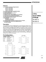
AT24C32/64
Features
•
•
•
•
•
•
•
•
•
•
•
•
Low Voltage and Standard Voltage Operation
5.0 (VCC = 4.5V to 5.5V)
2.7 (VCC = 2.7V to 5.5V)
2.5 (VCC = 2.5V to 5.5V)
1.8 (VCC = 1.8V to 5.5V)
Low Power Devices (ISB = 2 µA @ 5.5V) Available
Internally Organized 4096 x 8, 8192 x 8
2-Wire Serial Interface
Bidirectional Data Transfer Protocol
100 kHz (1.8V, 2.5V, 2.7V) and 400 kHz (5V) Compatibility
Write Protect Pin for Hardware Data Protection
32-Byte Page Write Mode (Partial Page Writes Allowed)
Self-Timed Write Cycle (10 ms max)
High Reliability
Endurance: 1 Million Cycles
Data Retention: 100 Years
Automotive Grade and Extended Temperature Devices Available
8-Pin JEDEC PDIP, 8-Pin and 14-Pin JEDEC SOIC and
8-Pin EIAJ Packages
2-Wire
Serial CMOS
E2PROM
32K (4096 x 8)
64K (8192 x 8)
Description
The AT24C32/64 provides 32,768/65,536 bits of serial electrically erasable and programmable read only memory (EEPROM) organized as 4096/8192 words of 8 bits
each. The device’s cascadable feature allows up to 8 devices to share a common
2-wire bus. The device is optimized for use in many industrial and commercial applications where low power and low voltage operation are essential. The AT24C32/64 is
available in space saving 8-pin JEDEC PDIP, 8-pin and 14-pin JEDEC SOIC and
8-pin EIAJ packages and is accessed via a 2-wire serial interface. In addition, the
entire family is available in 5.0V (4.5V to 5.5V), 2.7V (2.7V to 5.5V), 2.5V (2.5V to
5.5V) and 1.8V (1.8V to 5.5V) versions.
Pin Configurations
Pin Name
Function
A0 to A2
Address Inputs
SDA
Serial Data
SCL
Serial Clock Input
WP
Write Protect
AT24C32/64
8-Pin PDIP
14-Pin SOIC
8-Pin SOIC
0336D
2-49
Absolute Maximum Ratings*
Operating Temperature................... -55°C to +125°C
Storage Temperature...................... -65°C to +150°C
Voltage on Any Pin
with Respect to Ground ..................... -0.1V to +7.0V
*NOTICE: Stresses beyond those listed under “Absolute Maximum Ratings” may cause permanent damage to the device.
This is a stress rating only and functional operation of the
device at these or any other conditions beyond those indicated in the operational sections of this specification is not
implied. Exposure to absolute maximum rating conditions
for extended periods may affect device reliability.
Maximum Operating Voltage ........................... 6.25V
DC Output Current ......................................... 5.0 mA
Block Diagram
Pin Description
SERIAL CLOCK (SCL): The SCL input is used to positive
edge clock data into each E2PROM device and negative
edge clock data out of each device.
SERIAL DATA (SDA): The SDA pin is bidirectional for serial data transfer. This pin is open-drain driven and may be
wire-ORed with any number of other open-drain or open
collector devices.
DEVICE/PAGE ADDRESSES (A2, A1, A0): The A2, A1
and A0 pins are device address inputs that are hard wired
or left not connected for hardware compatibility with
AT24C16. When the pins are hardwired, as many as eight
32K/64K devices may be addressed on a single bus system (device addressing is discussed in detail under the
2-50
AT24C32/64
Device Addressing section). When the pins are not hardwired, the default A2, A1, and A0 are zero.
WRITE PROTECT (WP): The write protect input, when
tied to GND, allows normal write operations. When WP is
tied high to VCC, all write operations to the upper quandrant (8/16K bits) of memory are inhibited. If left unconnected, WP is internally pulled down to GND.
Memory Organization
AT24C32/64, 32K/64K SERIAL E2PROM: The 32K/64K
is internally organized as 256 pages of 32-bytes each.
Random word addressing requires a 12/13 bit data word
address.
AT24C32/64
Pin Capacitance (1)
Applicable over recommended operating range from TA = 25°C, f = 1.0 MHz, VCC = +1.8V.
Symbol
Test Condition
CI/O
CIN
Note:
Max
Units
Conditions
Input/Output Capacitance (SDA)
8
pF
VI/O = 0V
Input Capacitance (A0, A1, A2, SCL)
6
pF
VIN = 0V
1. This parameter is characterized and is not 100% tested.
DC Characteristics
Applicable over recommended operating range from: TAI = -40°C to +85°C, VCC = +1.8V to +5.5V, TAC = 0°C to +70°C,
VCC = +1.8V to +5.5V (unless otherwise noted).
Symbol Parameter
Test Condition
Min
Typ
Max
Units
VCC1
Supply Voltage
1.8
5.5
V
VCC2
Supply Voltage
2.5
5.5
V
VCC3
Supply Voltage
2.7
5.5
V
VCC4
Supply Voltage
4.5
5.5
V
ICC1
Supply Current VCC = 5.0V
READ at 100 kHz
0.4
1.0
mA
ICC2
Supply Current VCC = 5.0V
WRITE at 100 kHz
2.0
3.0
mA
ISB1
Standby Current
(1.8V option)
VCC = 1.8V
0.1
µA
ISB2
Standby Current
(2.5V option)
VCC = 2.5V
ISB3
Standby Current
(2.7V option)
VCC = 2.7V
ISB4 (1)
Standby Current
(5V option)
ILI
Input Leakage Current
ILO
Output Leakage Current
VIL
Input Low Level (2)
VIH
Input High Level (2)
VOL2
Output Low Level VCC = 3.0V
VOL1
Output Low Level VCC = 1.8V
VIN = VCC or VSS
VCC = 5.5V
2.0
0.5
VIN = VCC or VSS
VCC = 5.5V
2.0
0.5
VIN = VCC or VSS
VCC = 5.5V
µA
µA
2.0
VIN = VCC or VSS
20
35
µA
VIN = VCC or VSS
0.10
3.0
µA
VOUT = VCC or VSS
0.05
3.0
µA
-1.0
VCC x 0.3
V
VCC x 0.7
VCC + 0.5
V
IOL = 2.1 mA
0.4
V
IOL = 0.15 mA
0.2
V
VCC = 4.5 - 5.5V
Notes: 1. VCC lockout = 3.8V.
2. VIL min and VIH max are reference only and are not tested.
2-51
AC Characteristics
Applicable over recommended operating range from TA = -40°C to +85°C, VCC = +1.8V to +5.5V, CL = 1 TTL Gate and
100 pF (unless otherwise noted).
Symbol
Parameter
1.8-volt
Min
fSCL
Clock Frequency, SCL
tLOW
Clock Pulse Width Low
tHIGH
Clock Pulse Width High
2.7-, 2.5-volt
Max
Min
100
Max
5.0-volt
Min
100
Max
Units
400
kHz
4.7
4.7
1.2
µs
4.0
4.0
0.6
µs
(1)
tI
Noise Suppression Time
tAA
Clock Low to Data Out
Valid
0.1
tBUF
Time the bus must be free
before a new transmission
can start (1)
4.7
4.7
1.2
µs
tHD.STA
Start Hold Time
4.0
4.0
0.6
µs
tSU.STA
Start Set-up Time
4.7
4.7
0.6
µs
tHD.DAT
Data In Hold Time
0
0
0
µs
tSU.DAT
Data In Set-up Time
200
200
100
ns
Inputs Rise Time
tR
100
(1)
(1)
4.5
100
0.1
4.5
0.1
50
ns
0.9
µs
1.0
1.0
0.3
µs
300
300
300
ns
tF
Inputs Fall Time
tSU.STO
Stop Set-up Time
4.7
4.7
0.6
µs
tDH
Data Out Hold Time
100
100
50
ns
tWR
Write Cycle Time
Note:
20
10
10
ms
1. This parameter is characterized and is not 100% tested.
Device Operation
CLOCK and DATA TRANSITIONS: The SDA pin is normally pulled high with an external device. Data on the SDA
pin may change only during SCL low time periods (refer to
Data Validity timing diagram). Data changes during SCL
high periods will indicate a start or stop condition as defined below.
START CONDITION: A high-to-low transition of SDA with
SCL high is a start condition which must precede any
other command (refer to Start and Stop Definition timing
diagram).
STOP CONDITION: A low-to-high transition of SDA with
SCL high is a stop condition. After a read sequence, the
stop command will place the E2PROM in a standby power
mode (refer to Start and Stop Definition timing diagram).
2-52
AT24C32/64
ACKNOWLEDGE: All addresses and data words are serially transmitted to and from the E2PROM in 8 bit words.
The E2PROM sends a zero during the ninth clock cycle to
acknowledge that it has received each word.
STANDBY MODE: The AT24C32/64 features a low
power standby mode which is enabled: a) upon power-up
and b) after the receipt of the STOP bit and the completion
of any internal operations.
AT24C32/64
Bus Timing SCL: Serial Clock SDA: Serial Data I/O
Write Cycle Timing SCL: Serial Clock SDA: Serial Data I/O
Note:
1. The write cycle time tWR is the time from a valid stop condition of a write sequence to the end of the internal clear/write cycle.
2-53
Data Validity
Start and Stop Definition
Output Acknowledge
2-54
AT24C32/64
AT24C32/64
Device Addressing
E2PROM
The 32K/64K
requires an 8 bit device address
word following a start condition to enable the chip for a
read or write operation (refer to Figure 1). The device address word consists of a mandatory one, zero sequence
for the first four most significant bits as shown. This is
common to all 2-wire E2PROM devices.
The 32K/64K uses the three device address bits A2, A1, A0
to allow as many as eight devices on the same bus. These
bits must compare to their corresponding hardwired input
pins. The A2, A1, and A0 pins use an internal proprietary
circuit that biases them to a logic low condition if the pins
are allowed to float.
The eighth bit of the device address is the read/write operation select bit. A read operation is initiated if this bit is
high and a write operation is initiated if this bit is low.
Upon a compare of the device address, the E2PROM will
output a zero. If a compare is not made, the device will
return to standby state.
NOISE PROTECTION: Special internal circuitry placed
on the SDA and SCL pins prevent small noise spikes from
activating the device. A low-VCC detector (5-volt option)
resets the device to prevent data corruption in a noisy environment.
DATA SECURITY: The AT24C32/64 has a hardware data
protection scheme that allows the user to write protect the
upper quadrant (8/16K bits) of memory when the WP pin
is at VCC.
Write Operations
BYTE WRITE: A write operation requires two 8 bit data
word addresses following the device address word and
acknowledgement. Upon receipt of this address, the
E2PROM will again respond with a zero and then clock in
the first 8 bit data word. Following receipt of the 8 bit data
word, the E2PROM will output a zero and the addressing
device, such as a microcontroller, must terminate the write
sequence with a stop condition. At this time the E2PROM
enters an internally-timed write cycle to the nonvolatile
memory. All inputs are disabled during this write cycle and
the E2PROM will not respond until the write is complete
(refer to Figure 2).
PAGE WRITE: The 32K/64K E2PROM is capable of 32byte page writes.
A page write is initiated the same way as a byte write, but
the microcontroller does not send a stop condition after
the first data word is clocked in. Instead, after the
E2PROM acknowledges receipt of the first data word, the
microcontroller can transmit up to 31 more data words.
The E2PROM will respond with a zero after each data
word received. The microcontroller must terminate the
page write sequence with a stop condition (refer to Figure
3).
The data word address lower 5 bits are internally incremented following the receipt of each data word. The
higher data word address bits are not incremented, retaining the memory page row location. If more than 32 data
words are transmitted to the E2PROM, the data word address will “roll over” and previous data will be overwritten.
ACKNOWLEDGE POLLING: Once the internally-timed
write cycle has started and the E2PROM inputs are disabled, acknowledge polling can be initiated. This involves
sending a start condition followed by the device address
word. The read/write bit is representative of the operation
desired. Only if the internal write cycle has completed will
the E2PROM respond with a zero, allowing the read or
write sequence to continue.
Read Operations
Read operations are initiated the same way as write operations with the exception that the read/write select bit in
the device address word is set to one. There are three
read operations: current address read, random address
read and sequential read.
CURRENT ADDRESS READ: The internal data word address counter maintains the last address accessed during
the last read or write operation, incremented by one. This
address stays valid between operations as long as the
chip power is maintained. The address “roll over” during
read is from the last byte of the last memory page, to the
first byte of the first page. The address “roll over” during
write is from the last byte of the current page to the first
byte of the same page.
Once the device address with the read/write select bit set
to one is clocked in and acknowledged by the E2PROM,
the current address data word is serially clocked out. The
microcontroller does not respond with an input zero but
does generate a following stop condition (refer to Figure
4).
RANDOM READ: A random read requires a “dummy”
byte write sequence to load in the data word address.
Once the device address word and data word address are
clocked in and acknowledged by the E2PROM, the microcontroller must generate another start condition. The microcontroller now initiates a current address read by sending a device address with the read/write select bit high.
The E2PROM acknowledges the device address and serially clocks out the data word. The microcontroller does not
respond with a zero but does generate a following stop
condition (refer to Figure 5).
(continued)
2-55
Read Operations (Continued)
SEQUENTIAL READ: Sequential reads are initiated by
either a current address read or a random address read.
After the microcontroller receives a data word, it responds
with an acknowledge. As long as the E2PROM receives an
acknowledge, it will continue to increment the data word
address and serially clock out sequential data words.
Figure 1. Device Address
Figure 2. Byte Write
Figure 3. Page Write
(* = DON’T CARE bits)
(† = DON’T CARE bits for the 32K)
2-56
AT24C32/64
When the memory address limit is reached, the data word
address will “roll over” and the sequential read will continue. The sequential read operation is terminated when
the microcontroller does not respond with a zero but does
generate a following stop condition (refer to Figure 6).
AT24C32/64
Figure 4. Current Address Read
Figure 5. Random Read
(* = DON’T CARE bits)
Figure 6. Sequential Read
2-57
Ordering Information
tWR (max)
ICC (max)
ISB (max)
fMAX
(ms)
(µA)
(µA)
(kHz)
10
3000
35
400
AT24C32-10PC
AT24C32N-10SC
AT24C32W-10SC
AT24C32-10SC
8P3
8S1
8S2
14S
Commercial
(0°C to 70°C)
3000
35
400
AT24C32-10PI
AT24C32N-10SI
AT24C32W-10SI
AT24C32-10SI
8P3
8S1
8S2
14S
Industrial
(-40°C to 85°C)
1500
0.5
100
AT24C32-10PC-2.7
AT24C32N-10SC-2.7
AT24C32W-10SC-2.7
AT24C32-10SC-2.7
8P3
8S1
8S2
14S
Commercial
(0°C to 70°C)
1500
0.5
100
AT24C32-10PI-2.7
AT24C32N-10SI-2.7
AT24C32W-10SI-2.7
AT24C32-10SI-2.7
8P3
8S1
8S2
14S
Industrial
(-40°C to 85°C)
1000
0.5
100
AT24C32-10PC-2.5
AT24C32N-10SC-2.5
AT24C32W-10SC-2.5
AT24C32-10SC-2.5
8P3
8S1
8S2
14S
Commercial
(0°C to 70°C)
1000
0.5
100
AT24C32-10PI-2.5
AT24C32N-10SI-2.5
AT24C32W-10SI-2.5
AT24C32-10SI-2.5
8P3
8S1
8S2
14S
Industrial
(-40°C to 85°C)
800
0.1
100
AT24C32-10PC-1.8
AT24C32N-10SC-1.8
AT24C32W-10SC-1.8
AT24C32-10SC-1.8
8P3
8S1
8S2
14S
Commercial
(0°C to 70°C)
800
0.1
100
AT24C32-10PI-1.8
AT24C32N-10SI-1.8
AT24C32W-10SI-1.8
AT24C32-10SI-1.8
8P3
8S1
8S2
14S
Industrial
(-40°C to 85°C)
10
10
10
2-58
AT24C32/64
Ordering Code
Package
Operation Range
AT24C32/64
Ordering Information
Package Type
8P3
8 Lead, 0.300" Wide, Plastic Dual Inline Package (PDIP)
8S1
8 Lead, 0.150" Wide, Plastic Gull Wing Small Outline (JEDEC SOIC)
8S2
8 Lead, 0.200" Wide, Plastic Gull Wing Small Outline (EIAJ SOIC)
14S
14 Lead, 0.150" Wide, Plastic Gull Wing Small Outline (SOIC)
Options
Blank
Standard Operation (4.5V to 5.5V)
-2.7
Low Voltage (2.7V to 5.5V)
-2.5
Low Voltage (2.5V to 5.5V)
-1.8
Low Voltage (1.8V to 5.5V)
2-59
Ordering Information
tWR (max)
ICC (max)
ISB (max)
fMAX
(ms)
(µA)
(µA)
(kHz)
10
3000
35
400
AT24C64-10PC
AT24C64N-10SC
AT24C64W-10SC
AT24C64-10SC
8P3
8S1
8S2
14S
Commercial
(0°C to 70°C)
3000
35
400
AT24C64-10PI
AT24C64N-10SI
AT24C64W-10SI
AT24C64-10SI
8P3
8S1
8S2
14S
Industrial
(-40°C to 85°C)
1500
0.5
100
AT24C64-10PC-2.7
AT24C64N-10SC-2.7
AT24C64W-10SC-2.7
AT24C64-10SC-2.7
8P3
8S1
8S2
14S
Commercial
(0°C to 70°C)
1500
0.5
100
AT24C64-10PI-2.7
AT24C64N-10SI-2.7
AT24C64W-10SI-2.7
AT24C64-10SI-2.7
8P3
8S1
8S2
14S
Industrial
(-40°C to 85°C)
1000
0.5
100
AT24C64-10PC-2.5
AT24C64N-10SC-2.5
AT24C64W-10SC-2.5
AT24C64-10SC-2.5
8P3
8S1
8S2
14S
Commercial
(0°C to 70°C)
1000
0.5
100
AT24C64-10PI-2.5
AT24C64N-10SI-2.5
AT24C64W-10SI-2.5
AT24C64-10SI-2.5
8P3
8S1
8S2
14S
Industrial
(-40°C to 85°C)
800
0.1
100
AT24C64-10PC-1.8
AT24C64N-10SC-1.8
AT24C64W-10SC-1.8
AT24C64-10SC-1.8
8P3
8S1
8S2
14S
Commercial
(0°C to 70°C)
800
0.1
100
AT24C64-10PI-1.8
AT24C64N-10SI-1.8
AT24C64W-10SI-1.8
AT24C64-10SI-1.8
8P3
8S1
8S2
14S
Industrial
(-40°C to 85°C)
10
10
10
2-60
AT24C32/64
Ordering Code
Package
Operation Range
AT24C32/64
Ordering Information
Package Type
8P3
8 Lead, 0.300" Wide, Plastic Dual Inline Package (PDIP)
8S1
8 Lead, 0.150" Wide, Plastic Gull Wing Small Outline (JEDEC SOIC)
8S2
8 Lead, 0.200" Wide, Plastic Gull Wing Small Outline (EIAJ SOIC)
14S
14 Lead, 0.150" Wide, Plastic Gull Wing Small Outline (SOIC)
Options
Blank
Standard Operation (4.5V to 5.5V)
-2.7
Low Voltage (2.7V to 5.5V)
-2.5
Low Voltage (2.5V to 5.5V)
-1.8
Low Voltage (1.8V to 5.5V)
2-61