High-Efficiency High-Gain 2.4 GHz Class-B Power Amplifiers in 0.13 µm CMOS for Wireless Communications
Bạn đang xem bản rút gọn của tài liệu. Xem và tải ngay bản đầy đủ của tài liệu tại đây (713.64 KB, 7 trang )
VNU Journal of Science: Comp. Science & Com. Eng., Vol. 33, No. 1 (2017) 1-7
High-Efficiency High-Gain 2.4 GHz Class-B Power
Amplifiers in 0.13 µm CMOS for Wireless Communications
Tuan Anh Vu∗, Tuan Pham Dinh, Duong Bach Gia
VNU University of Engineering and Technology, Hanoi, Vietnam
Abstract
This paper presents high-efficiency high-gain 2.4 GHz power amplifiers (PAs) for wireless
communications. Two class-B PAs are designed and verified in 0.13 µm CMOS mixed-signal/RF process
provided by TSMC. The PAs employs cascode topologies with wideband multi-stage matchings. The singlestage cascode PA is designed for a high power added efficiency (PAE) of 35.4% while the gain is 20.4 dB
over the -3 dBbandwidth between 2.4 GHz and 2.48 GHz. The two-stage cascode PA is targeted for a high
gain of 37.7 dB while it exhibits a peak PAE of 24.1%. Supplied by 1.2 V supply voltages, the PAs consume
DC powers of 4.5 mW and 9 mW, respectively.
Received 28 December 2016; Accepted 20 February 2017
Keywords: Power Amplifier, Cascode, Multi-Stage, Wireless Communication.
1. Introduction*
transconductance. The linearity and power
efficiency
are
lower
than
other
technologies.However, with the trend of lower
power transmitters in the next generation,
implementation of CMOS PAs with good
efficiencies are becoming realistic despite
steadily declining field-effect transistor (FET)
breakdown voltages. To improve the efficiency
of the PAs, the trend is toward using class-B or
class-AB topologies, which are more energy
efficient compared to the class-A ones [2].
In this paper, we are going to present the
designs and simulations of two class-B 2.4 GHz
PAs suitable for wireless communication
standard including WiMAX, Bluetooth and
Wifi. The paper is organized as follows. Section
2 presents fundamentals of power amplifiers.
Section 3 introduces the architectures of the
proposed class-B PAs including detailed
descriptions of the circuit topologies. The
simulation results are presented in section 4 and
conclusions are given in the last section.
In today’s communication age, almost
every portable device has some sort of
transmitter and receiver allowing it to connect
to a cellular network or available Wi-Fi
networks. CMOS high-efficiency PAs are
among the most challenging components in
transmitter design for wireless communications,
automotive radar and other applications. The
main purpose of a PA design is to provide
sufficiently high output power, while another
very important target is to achieve high
efficiency. There are several obstacles which
make the implementations of a PA very
difficult in CMOS technology. The use of
submicron CMOS increases the difficulty of
implementation due to technology limitations
such as low breakdown voltage and poor
_______
*
Corresponding author. E-mail.:
/>
1
2
T.A. Vu et al. / VNU Journal of Science: Comp. Science & Com. Eng., Vol. 33, No. 1 (2017) 1-7
2. Poweramplifierbasics
2.1. PA block diagram
The general design concept of a PA is given
in Fig. 1. The two port network is applied in the
design consisting of two matching networks
that are used on both sides of the power
transistor. Maximum gain will be realized when
the matching networks provide a conjugate
match between the source/load impedance and
the transistor impedance [6]. Specifically, the
matching networks transform the input and
output impedance Z 0 to the source and load
impedances Z S and Z L , respectively. Both
input and output matching network are
designed for 50 Ωexternal load.
Figure 2. Operating points of the different classes
of current mode PAs [9].
The drain current I D exhibits pinch-off,
when the channel is completely closed by the
gate-source voltage VGS and reaches the
saturation, in which further increase of gatesource voltage results in no further increase in
drain current.
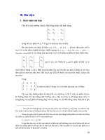
Table 1. Conduction angle of the different classes
of current mode PAs [9]
Class
A
AB
B
C
Figure 1. Block diagram of PAs.
2.2. Classification of PAs
There are generally two types of PAs: the
current source mode PAs and the switching
mode PAs. Different kinds of each mode of
PAs and their functional principles are
introduced in detail in [4]. In a current source
mode PA, the power device is regarded as a
current source, which is controlled by the input
signal. The most important current source mode
PAs are class A, class B, class AB and class C.
They differ from each other in the operating
points. Fig. 2 illustrates the different classes of
current source mode PAs in the transfer
characteristic of a FET device.
Conductance Angle
2
–2
0–
The other very important concept to define
the different classes of current source mode PA
is the conduction angle . The conduction
angle depicts the proportion of the RF cycle for
which conduction occurs. The conduction
angles of different classes are summarized in
table 1 while Fig. 3 shows an example of drain
voltage and current waveforms in an ideal
class-B PA.
2.3. PA efficiency
Efficiency is a measure of performance of
a PA. The performance of a PA will be better if
its efficiency is higher, irrespective of its
definition.
The
PA
is
the
most
power-consuming block in a wireless
transceiver.
T.A. Vu et al. / VNU Journal of Science: Comp. Science & Com. Eng., Vol. 33, No. 1 (2017) 1-7
Figure 3. Drain voltage and current waveforms
in an ideal class-B PA.
Its power efficiency has a direct impact on
the battery life of mobile devices. Several
definitions of efficiency are commonly used
with PAs. Most widely used measures are the
drain efficiency and power added efficiency.
The drain efficiency is defined as
POUT
(1)
PDC
where POUT is the RF output power at
operating frequency and PDC the DC power
=
consumption of the PA output stage. It reveals
how efficient the PA is when it converts the
power from DC to AC. The PAE is given by
PAE =
POUT PIN
PDC
(2)
where PIN is the input power fed to the PA
and PDC the total DC power consumption of
the PA. The PAE gets close to if the gain of
the PA is sufficient high so that the input power
is negligible.
Fig. 4 shows the complete circuit of the
single-stage cascode PA with all component
values are given in table 2. It includes an input
matching network, a cascode amplifying stage
and an output matching network. Apart from
the capability to deliver more output power, the
cascode stage alleviates the Miller effect and
therefore presents wider bandwidth and better
stability than common-source stage. Since PA
can be stabilized by maximizing their reverse
isolation, the cascode structure is employed in
this design to further increase input-output
reverse isolation and stability. For wideband
input and output matching, multi-stage
matchings using capacitors and inductors are
adopted. The capacitors and inductors form
4th-order high-pass filters at input and output
port. All of the capacitors also act as coupling
capacitors while the DC bias voltages are
applied across the inductors L2 and L3 .
On-chip inductors L1 , L2 , L3 and L4 have
values of 1.1, 2.8, 2.4 and 0.8 nH, respectively. To
operate as a class-B PA, the transistor M 1 is
biased with its gate-source voltage equals to the
threshold voltage, VGS = VTH = 420mV . A
235Ω resistor, RG , is added in series to the gate
of transistor M 1 for stabilization. The minimumloss cascade stabilizing resistor value is
determined from the Smith chart by finding the
constant resistance that is tangent to the
appropriate stability circle [5].
3. Design of 2.4 GHz class-B poweramplifiers
The PAs are designed using the TSMC
0.13µm CMOS mixed-signal/RF process. Its
back end consists of 8 copper layers and a top
aluminum redistribution layer (RDL). In order
to increase the efficiency, the designed PAs are
biased to operate as class-B PAs.
3.1. Single-Stage class-B cascode PA
3
Figure 4. The single-stage class-B cascode PA.
4
T.A. Vu et al. / VNU Journal of Science: Comp. Science & Com. Eng., Vol. 33, No. 1 (2017) 1-7
Table 2. Transistor Dimensions, Component
Values and Bias Setting of Single-Stage
Class-B Cascode PA
Parameter
Value
VDD
1.2 V
VGS
0.42 V
M1 – M 2
30µm/130nm
RG
235Ω
C1
C2
2.4 pF
C3
0.1 pF
C4
L1
L2
1.2 pF
1.1 nH
L3
2.4 nH
L4
0.8 nH
characteristic impedance of 71 Ω (the
71ΩGCPW-TL) is used for the shunt stubs of
the inter-stage matching network. The width of
the top-layer signal line is 3.2 µm, and the GND
wall
placed
at
a
distance
of 7.3 µm from the signal line has the width of
1.8µm. The 2nd to 4th metal layers are meshed
and stitched together with vias to form the
GND plane.
0.8 pF
2.8 nH
3.2. Two-Stage class-B cascode PA
The single-stage PA employs four on-chip
inductors in the input and output matching
network for bandwidth enhancement. These
inductors occupy a very large area in the layout
and are hard to adapt to finer pitch technology.
For two-stage PA, each inductor is replaced by
an equivalent transmission line (TL) for
reducing chip area. Although for 2.4 GHz
frequency band, the lengths of the TLs may be
long. However, the long TLs can be folded for
better area efficiency compared to the RF
inductor counterparts.
The cross-view of the grounded coplanar
wave-guide transmission line (GCPW-TL) is
depicted in Fig. 5. The GCPW-TL with a
characteristic impedance of Z 0 of 50 Ω (the 50
Ω GCPW-TL) is used for shunt stubs of the
input/output matching. Its signal line is
composed of the RDL layer with a width of 9.5
µm. Ground (GND) walls composed of the 5th
to 8th metal layers with a width of 2.7µm are
placed on the both side of the signal line at the
distance of 7µm. The GCPW-TL with
Figure 5. The cross-view of the GCPW
transmission line.
Fig. 6 show the complete circuit of the
two-stage cascode PA with all component
values are given in table 3. The cascode
topology reduces the input capacitance of the
second stage by decreasing the Miller effect due
to transistor M 1 . In order to double the gain, a
cascade of two cascode stages is used. The
capacitor C3 blocks the DC offset of the first
amplifying stage to have an independent
biasing of the second amplifying stage.
The DC bias voltages are established
through the transmission lines TL2 , TL3 , TL4
and TL5 . For stabilization, the resistor RG1 and
RG 2 is added in series to the gate of transistor
M1 and M 3 , respectively.
The lengths of the TLs and the capacitor
values are determined by a nonmetric
optimization process taking into account the
models of MOSFETs, MOM capacitors and
T.A. Vu et al. / VNU Journal of Science: Comp. Science & Com. Eng., Vol. 33, No. 1 (2017) 1-7
TLs. Many-stage amplifiers for RF
frequencies tend to occupy a large area since
inter-stage matching networks consist
typically of several passive devices that are
much large than MOSFETs.
5
71Ω GCPW-TLs themselves are designed to be
narrow, thereby reducing the footprint.
4. Simulation results
Simulated results of the class-B PAs for
TSMC 0.13 µm CMOS technology is achieved
using the CADENCE design environment.
Circuit design at high frequencies involves
more detailed considerations than at lower
frequencies when the effect of parasitic
capacitances and inductances can impose
serious constrains on achievable performance.
Figure 6. The two-stage class-B cascode PA.
Table 3. Transistor Dimensions, Component Values
and Bias Setting of Two-Stage Class-B Cascode PA
Parameter
Value
VDD
1.2 V
VGS
0.42 V
M1 – M 4
30µm/130nm
RG1 – RG 2
235 Ω
C1
C2
0.56 pF
C3
0.12 pF
C4
0.36 pF
C5
1.15 pF
TL1
TL2
658 µm
1662 µm
TL3
694 µm
TL4
1056 µm
TL5
TL6
936 µm
4.1. Single-Stage class-B cascode PA
Fig. 7 shows the simulated S-parameters of
the single-stage cascode PA. S11 remains below
17 dB while S 22 is less than 20 dB over a 3 dB bandwidth of 2.4–2.48 GHz. Both input
and output return loss indicate relatively
wideband performance.
0.22 pF
366 µm
To realize cost-effective chips, area
reduction is important. In order to reduce the
area of the amplifier, the 71 Ω GCPW-TLs used
in the inter-stage matching network are
arranged regularly at narrow spacings, and the
Figure 7. The simulated S-parameter
of the designed single-stage PA.
The PA achieves a peak gain of 20.4 dB at
2.45 GHz while the reverse isolation is lower
than -35 dB (not shown in the figure). A high
reverse isolation guarantees high stability for
the PA.
Fig. 8 and Fig. 9 show the drain efficiency
and PAE versus input power, respectively. The
designed PA obtains a peak drain efficiency of
36.6% at -10 dBm input power. It corresponds
to a peak PAE of 35.4%. The linearity of the
6
T.A. Vu et al. / VNU Journal of Science: Comp. Science & Com. Eng., Vol. 33, No. 1 (2017) 1-7
single-stage PA in term of input referred 1 dB
compression point (IP1dB) is -8.8 dBm. The
single-stage PA consumes only 4.5 mW from a
1.2 V supply voltage.
Figure 10. The simulated S-parameter of the
designed two-stage PA.
Fig. 11 and Fig. 12 show the drain
efficiency and PAE versus input power,
respectively. The peak drain efficiency drops to
25.4% corresponding to the peak PAE of 24.1%
at –21 dBm input power. The IP1dB is -24.5
dBm. The two-stage PA consumes only 9 mW
from a 1.2 V supply voltage. Table 4
summarizes the performance of the proposed
PAs and compares them to other published
designs operating in a similar frequency range.
Both proposed PAs are unconditionally stable
at all frequencies.
Figure 8. The simulated drain efficiency of the
designed single-stage PA.
Figure 9. The simulated PAE of the designed
single-stage PA.
4.2. Two-Stage Class-B Cascode PA
Fig. 10 shows the simulated S-parameters
of the two-stage cascode PA. S11 is less than
18 dB while S 22 is less than 15 dB over a 3 dB bandwidth from 2.4 GHz to 2.48 GHz.
The PA achieves a high gain of 37.7 dB at
2.45 GHz while the reverse isolation is lower
than -35 dB.
Figure 11. The simulated drain efficiency of the
designed two-stage PA.
J
Figure 12. The simulated PAE of the designed two-stage PA.
T.A. Vu et al. / VNU Journal of Science: Comp. Science & Com. Eng., Vol. 33, No. 1 (2017) 1-7
7
Table 4. Comparison with previous published PAs operating at 2.4 GHz band
Parameter
CMOS technology
Supply voltage (V)
Gain (dB)
Peak PAE (%)
IP1dB (dBm)
[3]
90 nm
3.3
28
33
0
[1]
[10]
[7]
[8]
This work 1 This work 2
65 nm 0.18 µm 0.18 µm 0.18 µm
0.13µm
0.13 µm
3.3
5.6
1.8
2.4
1.2
1.2
32
21.4
10.4
18
20.4
37.7
25
26.1
16.2
24.6
35.4
24.1
7
5.6
13
7.5
-8.8
-24.5
p
5 Conclusions
In this paper, we have presented the design
and simulation of high-efficiency high-gain 2.4
GHz PAs. Two class-B cascode PAs are
designed in TSMC 0.13µm CMOS mixedsignal/RF process. The performances of the
PAs are verified by simulation results, and are
competitive to other state-of-the-art PAs in
CMOS. Both designed PAs are suitable for
wireless communication standards including
WiMAX,Bluetooth and Wifi.
Acknowledgements
This work has been supported by VNU
University of Engineering and Technology,
under Project No. CN.15.04.
References
[1] A. Afsahi, A. Behzad, and L. E. Larson, “A
65nm cmos 2.4ghz 31.5dbm power amplifier
with a distributed lc power-combining network
and
improved
linearization
for
wlan
applications,”
2010
IEEE
International
Solid-State Circuits Conference, pp. 452–453,
February 2010.
[2] M. Bozanic and S. Sinha, Power amplifiers for
the s-, c-, x- and ku-bands - an eda perspective.
Springer International Publishing, 2016.
[3] D. Chowdhury, C. D. Hull, O. B. Degani, and Y.
Wang, “A fully integrated dual-mode linear
2.4ghz cmos power amplifier for 4g wimax
applications,” IEEE Journal of Solid-State
Circuits, vol. 44, no. 12, pp. 3393-3402,
December 2009.
[4] S. C. Cripps, Rf power amplifier for wireless
communications. Artech House, Inc., 1999.
[5] R. Gilmore and L. Besser, Practical rf circuit
design for modern wireless systems - volume
ii: active circuits and systems. Artech House
Inc., 2003.
[6] G.
Gonzalez,
Microwave
transistor
amplifiers - analysis and design/second edition.
Prentice Hall, Inc., 1997.
[7] H. Magnusson and H. Olsson, “A compact
dual-band power amplifier driver for 2.4ghz and
5.2ghz wlan transmitters,” 2007 IEEE Radio
Frequency Integrated Circuits Symposium,
pp. 83-86, June 2007.
[8] C.-C. Huang and W.-C. Lin, “A compact highefficiency cmos power amplifier with built-in
linearizer,” IEEE Microwave and Wireless
Components Letters, vol. 19, no. 9, pp. 587-589,
September 2009.
[9] L. Wu, Design of radio frequency power
amplifiers for cellular phones and base stations
in modern mobile communication system, Ph. D.
thesis. University of Stuttgart, 2009.
[10] Y. Yin, B. Chi, X. Yu, W. Jia, and Z. Wang,
“An efficiency-enhanced 2.4ghz stacked cmos
power amplifier with mode switching scheme
for wlan applications,” IEEE 2014 Custom
Integrated Circuits Conference, pp. 1-4,
September 2014.